

Page 1
QUADRATURE CLOCK CONVERTER
FEATURES:
• x1, x2 and x4 mode selection
• Up to 16 MHz output clock frequency
• INDEX input and output
• UP/DOWN indicator output
• Programmable output clock pulse width
• On-chip filtering of inputs for optical or
magnetic encoder applications.
• TTL and CMOS compatible I/Os
• +4.5V to +10.0V operation (VDD-VSS)
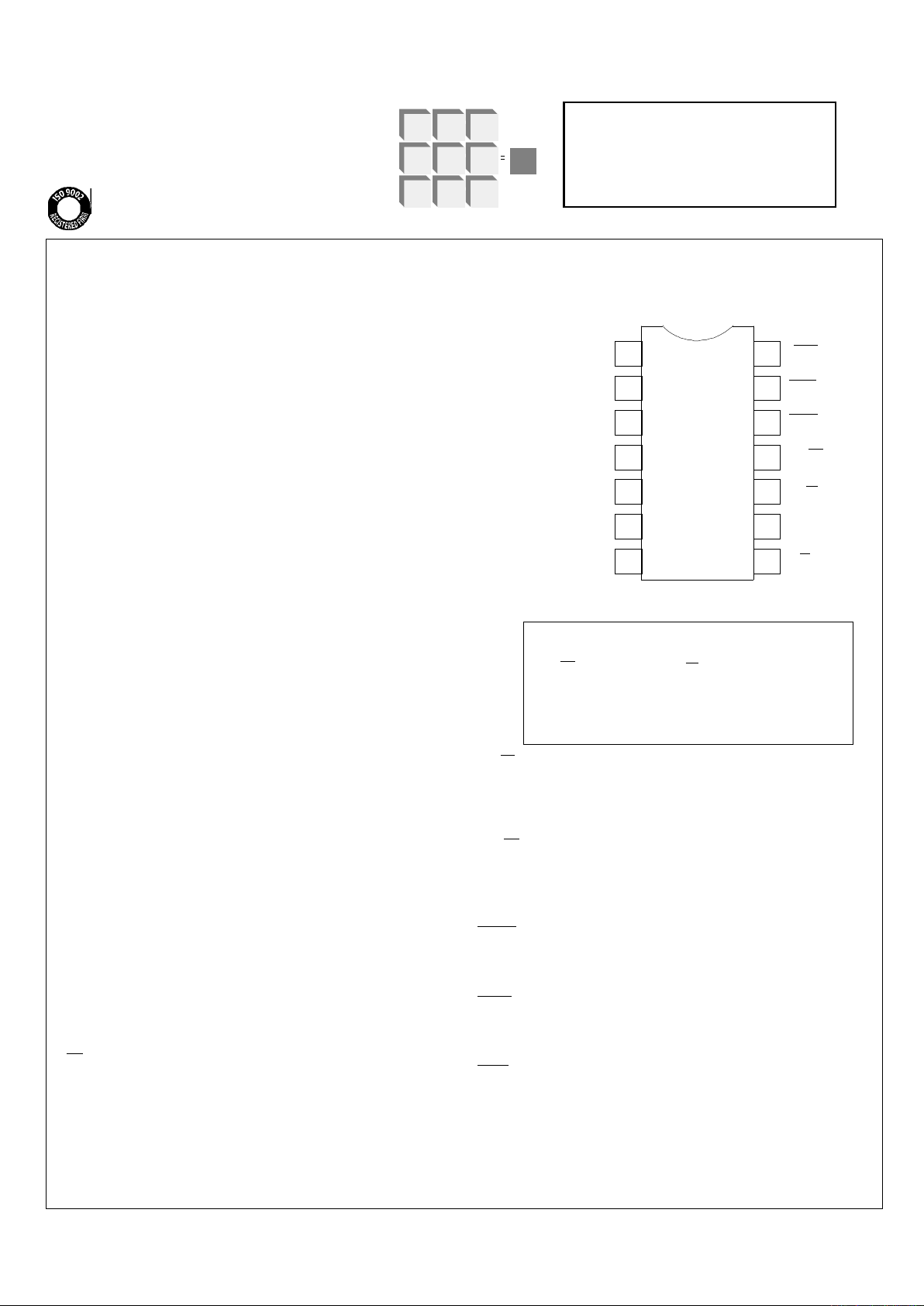
• LS7082 (DIP), LS7082-S (SOIC )- See Figure 1
INPUT/OUTPUT DESCRIPTION:
VDD (Pin 1)
Supply Voltage positive terminal.
INDX (Pin 2)
Encoder Index pulses are applied to this input.
RBIAS (Pin 3)
Input for external component connection. A resistor connected between this input and VSS adjusts the output clock
pulse width (Tow). For proper operation, the output clock
pulse width must be less than or equal to the A,B pulse
separation (TOW ≤ TPS).
VSS (Pin 4)
Supply Voltage negative terminal.
A (Pin 5)
Quadrature Clock Input A. This input has a filter circuit to
validate input logic level and eliminate encoder dither.
x2 (Pin 8)
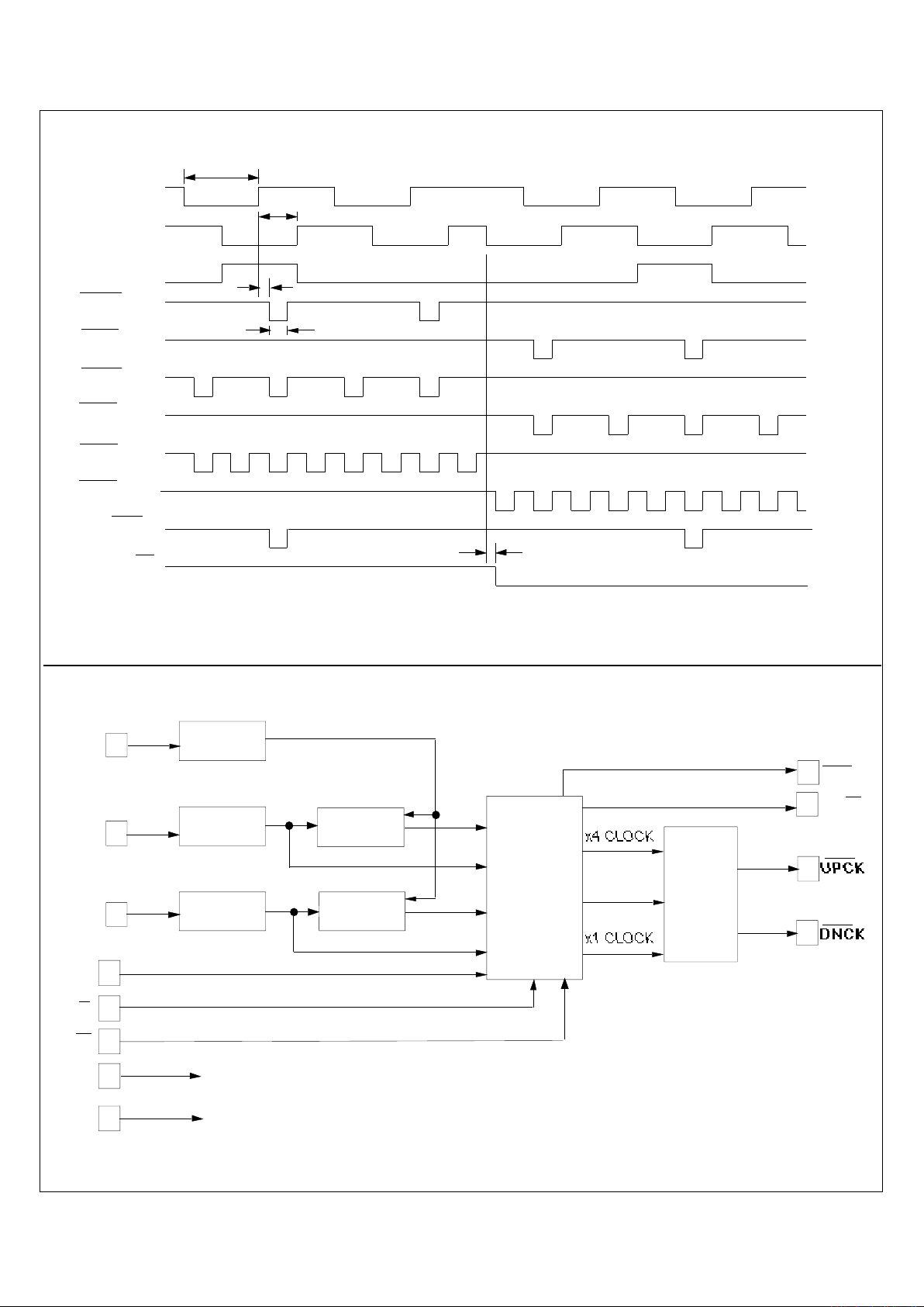
A low level applied to this input selects x2 mode of operation. See Table 1 for Mode Selection Truth Table and
Figure 2 for Input/Output timing relationship.
B (Pin 9)
Quadrature Clock Input B. This input has a filter circuit
identical to input A.
x4/x1 (Pin 10)
This input selects between x1 and x4 modes of operation.
See Table 1 for Mode Selection Truth Table and Figure 2
for Input/Output timing relationship.
UP/DN (Pin 11)
The count direction at any instant is indicated at this output. An UP count direction is indicated by a high, and a
DOWN count direction is indicated by a low (See Figure 2).
DNCK (Pin 12)
This DOWN Clock output consists of low-going pulses generated when A input lags the B input (See Figure 2).
UPCK (Pin 13)
This UP Clock output consists of low-going pulses generated when A input leads the B input (See Figure 2).
INDX (Pin 14)
This output consists of low-going pulses generated by
clock transitions at the A input when INDX input is high and
B input is low (See Figure 2).
NOTE: All unused input pins must be tied to VDD or VSS.
DESCRIPTION:
The LS7082 is a monolithic CMOS silicon gate quadrature
clock converter. Quadrature clocks derived from optical or
magnetic encoders, when applied to the A and B Inputs of the
LS7082, are converted to strings of Up Clocks and Down
Clocks. Pulses derived from the Index Track of an encoder,
when applied to the INDX input, produce absolute position reference pulses which are synchronized to the Up Clocks and
Down Clocks. These outputs can be interfaced directly with
standard Up/Down counters for direction and position sensing
of the encoder.
October 2000
1
2
3
4
5
6
7
LS7082
INDX
UPCK
DNCK
UP/DN
x4/x1
B
x2
VDD (+V)
INDX
RBIAS
VSS (-V)
A
NC
NC
14
13
12
11
8
9
10
FIGURE 1
PIN ASSIGNMENT - TOP VIEW
LSI
7082-100600-1
TABLE 1. MODE SELECTION TRUTH TABLE
x2 Input x4/x1 Input MODE
0 Don’t Care x2
1 0 x1
1 1 x4
LSI/CSI
LSI Computer Systems, Inc. 1235 Walt Whitman Road, Melville, NY 11747 (631) 271-0400 FAX (631) 271-0405
LS7082
U
L
®
A3800
Page 2

ABSOLUTE MAXIMUM RATINGS:
PARAMETER SYMBOL VALUE UNITS
DC Supply Voltage VDD - VSS 11.0 V
Voltage at any input VIN VSS -.3 to VDD +.3 V
Operating temperature TA 0 to +70 °C
Storage temperature TSTG -55 to +150 °C
DC ELECTRICAL CHARACTERISTICS:
(All voltages referenced to VSS, TA = 0°C to 70°C.)
PARAMETER SYMBOL MIN MAX UNITS CONDITION
Supply voltage VDD 4.5 10.0 V Supply current IDD - 6.0 µA VDD = 10.0V, All
input frequencies = 0 Hz
RBIAS = 2MΩ
x4/x1, x2, INDX Logic Low VIL - 0.3VDD V -
A,B Logic Low VIL - 0.6 V VDD = 4.5V
- 1.0 V VDD = 9V
- 1.1 V VDD = 10.0V
x4/x1, x2, INDX Logic High VIH 0.7VDD - V -
A,B Logic High VIH 3.1 - V VDD = 4.5V
5.0 - V VDD = 9V
5.6 - V VDD = 10.0V
ALL OUTPUTS:
Sink Current IOL 1.75 - mA VDD = 4.5V
VOL = 0.4V 5.0 - mA VDD = 9V
5.7 - mA VDD = 10.0V
Source Current IOH 1.0 - mA VDD = 4.5V
VOH = VDD - 0.5V 2.5 - mA VDD = 9V
3.0 - mA VDD = 10.0V
TRANSIENT CHARACTERISTICS:
(TA = 0°C to 70°C)
PARAMETER SYMBOL MIN MAX UNITS CONDITION
A,B inputs:
Validation Delay TvD - 85 ns VDD = 10.0V
- 100 ns VDD = 9V
- 160 ns VDD = 4.5V
A,B inputs:
Pulse Width TPW TVD+TOW Infinite ns -
A to B or B to A
Phase Delay TPS TOW Infinite ns -
1
A,B frequency fA,B - 2TPW Hz -
Input to Output Delay TDS - 120 ns VDD = 10.0V
- 150 ns VDD = 9V
- 235 ns VDD = 4.5V
Includes input
validation delay
Output Clock Pulse Width TOW 50 - ns See Fig. 4 & 5
7082-100600-2
Page 3
MUX
CLOCK
AND
DIRECTION
DECODE
DUAL
ONE-SHOT
DUAL
ONE-SHOT
CURRENT
MIRROR
VDD
FIGURE 3. LS7082 BLOCK DIAGRAM
x2 CLOCK
14
11
13
12
UP/DN
x2
3
5
9
10
8
1
4
2
INDX
A
B
INDX
VSS
FILTER
RBIAS
+V
-V
x4/x1
FILTER
7082-100100-3
UPCK (x2)
A
B
INDX
UPCK (x1)
DNCK (x1)
DNCK (x2)
UPCK (x4)
INDX
UP/DN
TPW
TDS
TPS
Tow
TDS
FIGURE 2. LS7082 INPUT/OUTPUT TIMING DIAGRAM
DNCK (x4)
Page 4
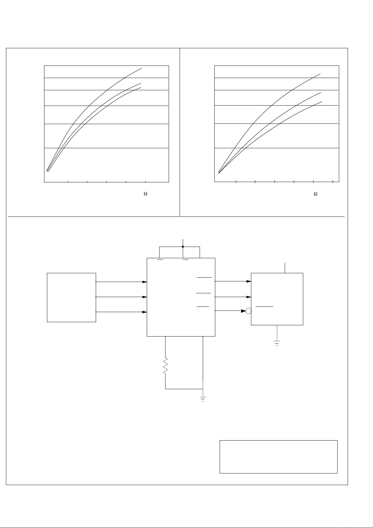
Figure 4. Tow vs RBIAS, K
VDD=5V
VDD=9V
VDD=10.0V
100
200
300 400 500
250
500
750
1000
1250
1500
OUTPUT CLOCK PULSE WIDTH, Tow, ns
ENCODER
A CLOCK
B CLOCK
INDEX
5
9
2
13
12
14
8
10 1
3 4
RB
UPCK
DNCK
RESET
x2 x4/x1
VDD
A
B
RBIAS
VSS
UPCK
DNCK
INDX
FIGURE 6. A TYPICAL APPLICATION IN x4 MODE
VSS
VDD
LS7082
5
4
14
16
8
+V
40193
+V
INDX
VDD=5V
VDD=9V
VDD=10.0V
25
30
20
15
10
5
2
4
6
8
10
12
Figure 5. Tow vs RBIAS, M
OUTPUT CLOCK PULSE WIDTH, Tow, µs
The information included herein is believed to be
accurate and reliable. However, LSI Computer Systems,
Inc. assumes no responsibilities for inaccuracies, nor for
any infringements of patent rights of others which may
result from its use.
7082-100100-4
 Loading...