

Page 1
B3 OUT
B6 IN
B2 OUT
B5 IN
B1 OUT
B4 IN
B0 OUT
LSI/CSI
LSI Computer Systems, Inc. 1235 Walt Whitman Road, Melville, NY 11747 (631) 271-0400 FAX (631) 271-0405
LS7061/7063
SCAN RESET/LOAD
U
L
®
A3800
32 BIT/DUAL 16 BIT BINARY UP COUNTER
WITH BYTE MULTIPLEXED THREE-STATE OUTPUTS
Aug. 1998
FEATURES:
• DC to 15 MHz Count Frequency
• Byte Multiplexer
• DC to 1 MHz Scan Frequency
• +4.75V to +5.25V Operation (VDD-VSS)
• Latch Provided for External High Speed Counter Byte,
Effectively Extending Count Frequency to 3.84GHz
• Three-State Data Outputs, Bus and TTL Compatible
• Inputs TTL and CMOS Compatible
• Unique Cascade Feature Allows Multiplexing of
Successive Bytes of Data in Sequence in Multiple
Counter Systems
• LS7061, LS7063 (DIP); LS7061-S, LS7063-S (SOIC)
(See Figures 1 & 2)
DESCRIPTION:
The LS7061/LS7063 is a monolithic, ion implanted MOS Silicon
Gate, 32 bit/dual 16 bit up counter. The IC includes 40 latches,
multiplexer, eight three-state binary data output drivers and output cascading logic.
DESCRIPTION OF OPERATION:
32 (16) BIT BINARY UP COUNTER - LS7061 (LS7063)
The 32 (16) bit static ripple through counter increments on the
negative edge of the input count pulse. Maximum ripple time is
4µs (2µs) - transition count of 32 (16) ones to 32 (16) zeros.
Guaranteed count frequency is DC to 15MHz.
See Figure 8A (8B) for Block Diagram.
COUNT - LS7061, COUNT A - LS7063
Input count pulses to the 32 (first 16) bit counter may be applied
through this input. This input is the most significant bit of the external data byte.
COUNT B - LS7063
Count pulses may be applied to the last 16 bits of the binary
counter through this input. The counter advances on the negative
transition of these pulses.
RESET
All 32 counter bits are reset to zero when RESET is brought low
for a minimum of 1µs. RESET must be high for a minimum of
300ns before next valid count can be recorded. COUNT B must
be held low when RESET is brought low to ensure proper reset of
Counter B for LS7063.
TEST COUNT - LS7061
Count pulses may be applied to the last 16 bits of the binary
counter through this input, as long as Bit 16 of the counter is a
low. The counter advances on the negative transition of these
pulses. This input is intended to be used for test purposes.
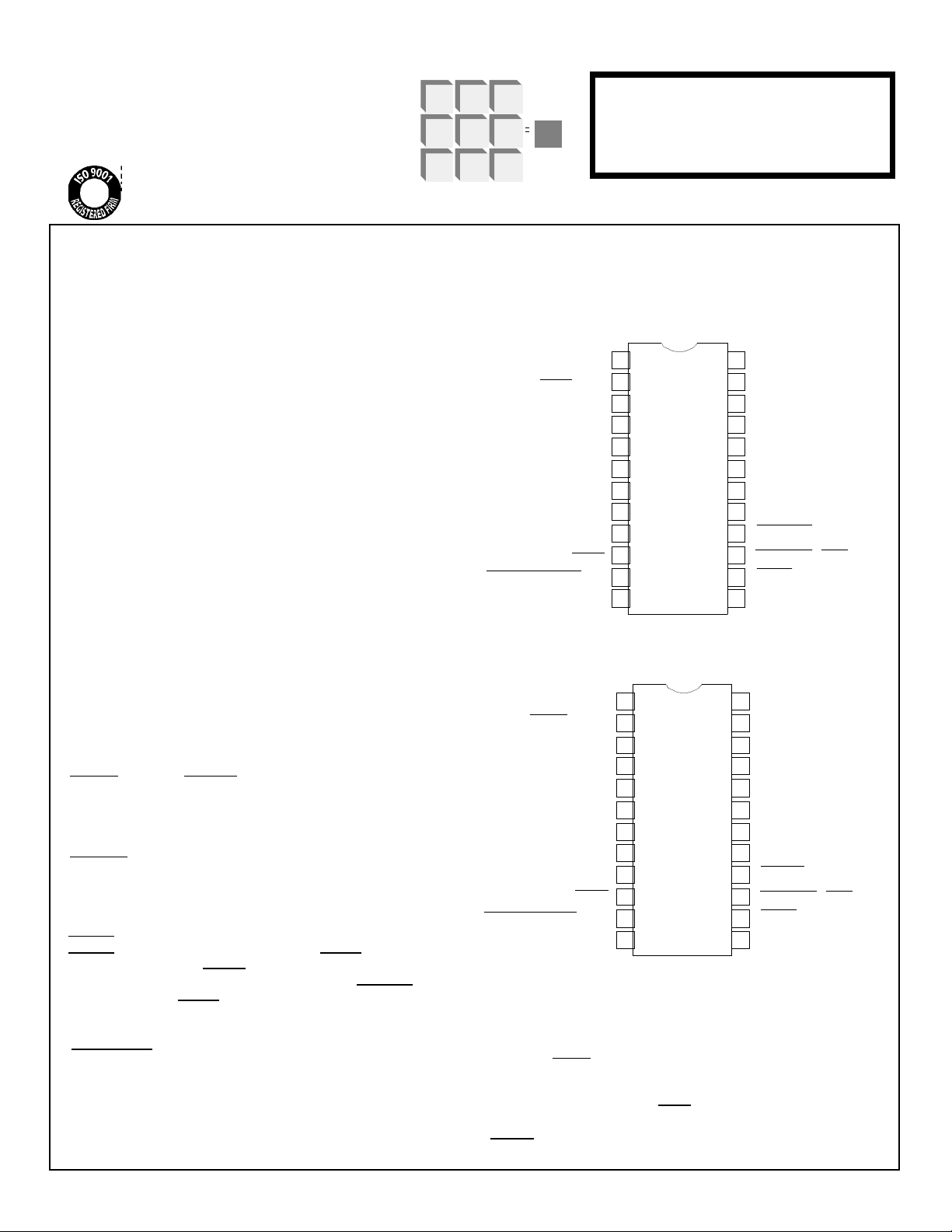
PIN ASSIGNMENT - TOP VIEW
LSI
VDD (+V)
(COUNT) B7 IN
RESET
CASCADE ENABLE OUT
Vss (-V)
VDD (+V)
(COUNTA) B7 IN
B3 OUT
B6 IN
B2 OUT
B5 IN
B1 OUT
B4 IN
B0 OUT
RESET
CASCADE ENABLE OUT
Vss (-V)
1
2
3
4
5
LS7061
6
7
8
9
10
11
12
FIGURE 1
PIN ASSIGNMENT - TOP VIEW
LSI
1
2
3
4
5
LS7063
6
7
8
9
10
11
12
FIGURE 2
24
B4 OUT
23
B5 OUT
22
B0 IN
21
B1 IN
20
B6 OUT
19
B2 IN
18
B7 OUT
17
B3 IN
16
TEST COUNT
15
SCAN RESET/LOAD
14
ENABLE
13
SCAN
24
B4 OUT
23
B5 OUT
22
B0 IN
21
B1 IN
20
B6 OUT
19
B2 IN
18
B7 OUT
17
B3 IN
16
COUNT B
15
14
ENABLE
13
SCAN
LATCHES - LS7061 (LS7063)
40 bits of latch are provided, eight for storage of the contents
of a high speed external prescaling counter and the remaining
32 for the contents of the counter data. All latches are loaded
when the LOAD input is brought low for a minimum of 1µs
and kept low until a minimum of 4µs (2µs) has elapsed from
previous negative edge of count pulse (ripple time). Storage
of valid data occurs when LOAD is brought high for a minimum of 250ns before next negative edge of count pulse or
RESET.
7061/63-083198-1
Page 2
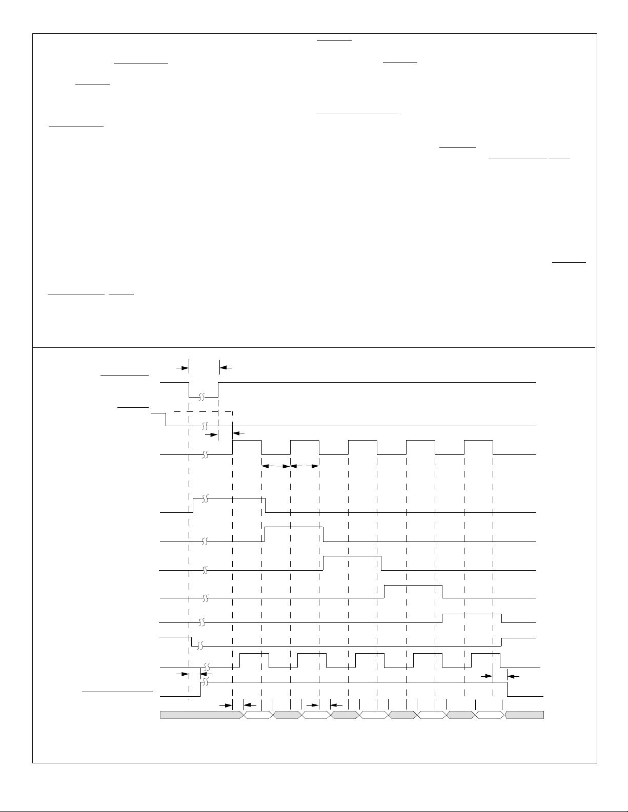
SCAN COUNTER AND DECODER
7061/63-083198-2
The scan counter is reset to the least significant byte position
(State 1) when SCAN RESET input is brought low for a minimum of 1µs. The scan counter is enabled for counting as long
as the ENABLE input is held low. The counter advances to the
next significant byte position on each negative transition of the
SCAN pulse. When the scan counter advances to State 6 it disables the Output Drivers and stops in that state until
SCAN RESET is again brought low.
SCAN
When the scan counter is enabled, each negative transition of
this input advances the scan counter to its next state. When
SCAN is low the Data Outputs are disabled. When SCAN is
brought high the Data Outputs are enabled and present the
latched counter data corresponding to the present state of the
scan counter. Therefore, in microprocessor applications, the
Data Output Bus may be utilized for other activities while new
data is propagating to the outputs. This positive SCAN pulse
can be viewed as a "Place the next byte on my bus" instruction
from the microprocessor. Minimum positive and negative pulse
widths of 500ns for the SCAN signal are required for scan
counter operation.
SCAN RESET/LOAD
When this input is brought low for a minimum of 1µs, the scan
counter is reset to State 1, the least significant byte position,
and the latches are simultaneously loaded with new count
information.
ENABLE
When this input is high, the scan counter and the Data Outputs are
disabled. When ENABLE is low, the scan counter and Data Outputs are enabled for normal operation. Transition of this input
should only be made while the SCAN input is in a low state in order
to prevent false clocking of the scan counter.
CASCADE ENABLE
This output is normally high. It transitions low and stays low when
the scan counter advances to State 6. In a multiple counter system
this output is connected to the ENABLE input of the next counter in
the cascade string. The SCAN input and SCAN RESET/LOAD input are carried to all the counters in the "Cascade". Counter 1 then
presents its bytes of data to the Output Bus on each positive transition of the SCAN pulse as previously discussed. When State 6 of
Counter 1 is achieved, Counter 2 presents its data to the Output
Bus. This sequence continues until all counters in the cascade
have been addressed. See Figure 5 for an illustration of a 3 device
cascade design. This output is TTL and CMOS compatible.
THREE-STATE DATA OUTPUT DRIVERS
The eight Data Output Drivers are disabled when either ENABLE
input is high, the scan counter is in State 6, or the SCAN input is
low. The Output Drivers are TTL and Bus compatible.
SCAN RESET
ENABLE
SCAN
ST1 (int.)
ST2 (int.)
ST3 (int.)
ST4 (int.)
ST5 (int.)
ST6 (int.)
tRSCPW
tRSCR
tSCPW
tSCPW
ENABLE (int.)
ENABLE (int.)
CASCADE ENABLE
DATA OUTPUTS
FIGURE 3. SCAN COUNTER & DECODER OUTPUTS TIMING DIAGRAM
tDCE
tDOE
valid
LSB
LSB+1
tDOD
LSB +2
validvalidvalid
LSB+3
tDCE
valid
MSB
Page 3
ABSOLUTE MAXIMUM RATINGS:
Input Current
*SCAN RESET/LOAD IIH - -2.5 µA VDD = Max, VIH = +3.5
IIL - -5 µA VDD = Max, VIL = 0
**B0-B7, COUNT B, IIH - 5 µA VDD = Max, VIH = +3.5
TEST COUNT
IIL - 1 µA VDD = Max, VIL = 0
*Input has internal pull-up resistor to VDD
** Inputs have internal pull-down resistor to VSS
7061/63-090198-3
PARAMETER SYMBOL VALUE UNIT
StorageTemperature TSTG -55 to +150 °C
Operating Temperature TA 0 to +70 °C
Voltage (any pin to VSS) VIN +10 to -0.3 V
DC ELECTRICAL CHARACTERISTICS:
(VDD = +5V ± 5%, VSS = 0V, TA = 0˚C to + 70˚C unless otherwise noted.)
PARAMETER SYMBOL Min MAX UNIT CONDITIONS
Power Supply Current IDD - 15 mA At Maximum Operating Frequency
VDD = Max, Outputs No Load
Input High Voltage VIH +3.5 VDD V Input Low Voltage VIL 0 +0.6 V -
Output High Voltage
CASCADE ENABLE VOH VDD-0.2 - V IO = 0, VDD = Min
+2.4 - V IO = -100µA, VDD = Min
B0 - B7 +2.4 - V IO = -260µA, VDD = Min
+2.0 - V IO = -750µA, VDD = Min
Output Low Voltage
CASCADE ENABLE VOL - +0.2 V IO = 0, VDD = Min
+0.4 V IO = 1.6mA, VDD = Min
B0 - B7 +0.4 V IO = 1.6mA, VDD = Min
Output Source Current Isource 3.0 - mA VO = +1.2V, VDD = Min
B0 - B7 Outputs 4.8 - mA VO = +0.8V, VDD = Min
7.3 - mA VO = +0.4V, VDD = Min
Output Sink Current Isink 5.7 - mA VO = +1.2V, VDD = Min
B0 - B7 Outputs 4.0 - mA VO = +0.8V, VDD = Min
2.2 - mA VO = +0.4V, VDD = Min
Output Leakage Current IOL - 1 µA VO = +.4V to +2.4V,VDD = Min
B0 - B7 (Off State)
Input Capacitance CIN - 6 pF TA = 25˚C, f = 1MHz
Output Capacitance COUT - 12 pF TA = 25˚C, f = 1MHz
Input Leakage Current ILI - 1 µA VDD = Max
ENABLE, RESET, SCAN
The information included herein is believed to be
accurate and reliable. However, LSI Computer Systems,
Inc. assumes no responsibilities for inaccuracies, nor for
any infringements of patent rights of others which may
result from its use.
Page 4

DYNAMIC ELECTRICAL CHARACTERISTICS: (Refer to Figure 3, Timing Diagram)
7061/63-083198-4
(VDD = +5V ± 5%, VSS = 0V, TA = 0˚C to +70˚C unless otherwise noted.)
PARAMETER SYMBOL MIN MAX UNIT CONDITIONS
Count Frequency fc DC 15 MHz (All Count inputs)
Count Pulse Width tCPW 30 - ns Measured at 50% point,
(All Count Inputs) Max tr, tf = 10ns
Count Rise & Fall time tr, tf - 30 µs -
(Pins 2, 16)
Count Ripple Time tCR - 4 µs Transition from32 ones to 32 zeros
(Pins 2 - LS7061) from negative edge of count pulse
Count Ripple Time tCR - 2 µs Transition of 16 bits from
(Pin 13 - LS7061) all ones to all zeros from negative edge
(Pins 2,13 - LS7063) of count pulse
RESET Pulse Width tRPW 500 - ns Measured at 50% point
(All Counter Stages Max tr, tf = 200ns
Fully Reset)
RESET Removal Time tRR - 250 ns Measured from RESET signal at VIH
(Reset Removed From
All Counter Stages)
SCAN Frequency fSC - 1 MHz
SCAN Pulse Wildth tSCPW 500 - ns Measured at 50% point
Max tr, tf = 100ns
SCAN RESET/LOAD tRSCPW 1 - µs Measured at 50% point
Pulse Width Max tr, tf = 200ns
(All latches loaded and
Scan Counter Reset to
Least Significant Byte)
SCAN RESET/LOAD tRSCR - 250 ns Measured from SCAN RESET/
Removal Time LOAD at VIH
(Reset Removed from
Scan Counter; Load
Command Removed
From Latches)
Output Disable tDOD - 200 ns Transition to Output High
Delay Time Impedance State Measured
(B0 - B7) From Scan at VIL or
ENABLE at VIH
Output ENABLE tDOE - 200 ns Transition to Valid On State
Delay Time Measured from Scan at VIH
(B0 - B7) and ENABLE at VIL; Delay to
Valid Data Levels for COL =10pF
and one TTL Load or Valid Data
Currents for High Capacitance Loads
Output Delay Time tDCE - 300 ns Negative Transition from Scan at VIL
CASCADE ENABLE and ST5 of Scan Counter or Positive
Transition From SCAN RESET/LOAD at
VIL to Valid Data Levels for COL = 10pF
and one TTL Load
Page 5

RESET
tRPW
tRPW
COUNT
LOAD
tCPW
tRR + tCPW
tRSCR
tCR
FIGURE 4. COUNTER TIMING DIAGRAM
tRR+tCPW
tCPW
tRSCPW
ENABLE
SCAN RESET
7061/63-083198-5
SCAN
A
EN SC RESET SC
CE
OUTPUT DATA BUS
B
EN SC RESET SC
FIGURE 5. ILLUSTRATION OF A 3 DEVICE CASCADE
CE
C
EN SC RESET SC
CE
END OF SCAN
Page 6

SCAN RESET
ENABLE
SCAN
CASCADE ENABLE A
CASCADE ENABLE B
CASCADE ENABLE C
(END OF SCAN)
DATA BYTE ON BUS
PACKAGE
1
2 3 4 5
A
FIGURE 6. TIMING DIAGRAM FOR THE 3 DEVICE CASCADE
1 2
3 4 5B1 2 3 4
C
5
FIGURE 7. APPLICATION EXAMPLE: HIGH SPEED DIFFERENTIAL ENERGY ANALYZER
LS7061 OR LS7063
DETECTOR
RADIATION
PULSE
Pulse voltage
proportional
to energy of
radiation
VOLTAGE
DISCRIMINATORS
PRESCALERS
EN
CE
EN
CE
EN
CE
CASCADE ENABLE
SCAN
B
U
S
PROCESSOR
NOTE : The processor subtracts counts from successive counters to determine
the differential energy spectrum
7061/63-083198-6
Page 7

1
VDD
VSS
12
ENABLE
SCAN
SCAN RESET/LOAD
FIGURE 8A. LS7061 BLOCK DIAGRAM
CASCADE ENABLE
11
+V
-V
DECODER
ST2
6 STATE
ST3
ST4 ST5
14
13
15
STATIC SCAN COUNTER AND
CSC
(STOPS IN STATE 6 UNTIL SCAN RESET
CAUSES RESET TO STATE ONE)
RSC
ST1
ST6
ENABLE
DATA OUT
LSB MSB
B0
B1 B2 B3 B4 B5 B6 B7
9 7 5 3 24 23 20 18
THREE STATE
EN
OUTPUT DRIVERS
8 BITS
8 BIT MUX BUS
MUX
G
GATE
8 BIT LATCH
22 19
8
B0B1B2
B3B4B5B6B7
DATA IN
1
VDD
VSS
12
ENABLE
SCAN
SCAN RESET/LOAD
LOAD
4
14
13
15
221 17 6
+V
-V
(COUNT)
MUX
G
GATE
LOAD
8 BIT LATCH
B0 B7
8 BIT BINARY
COUNTER
C
R
MUX
G
GATE
8 BIT LATCH
LOAD
B0 B7 B0 B7 B0 B7
8 BIT BINARY
COUNTER
C
R
FIGURE 8B. LS7063 BLOCK DIAGRAM
STATIC SCAN COUNTER AND
CSC
(STOPS IN STATE 6 UNTIL SCAN RESET
CAUSES RESET TO STATE ONE)
RSC
ST1
6 STATE
DECODER
ST2
ST3
ST4
16
TEST COUNT
ST6
ST5
LOAD
C
G
R
MUX
GATE
8 BIT LATCH
8 BIT BINARY
COUNTER
CASCADE ENABLE
11
ENABLE
MUX
G
GATE
8 BIT LATCH
LOAD
8 BIT BINARY
COUNTER
C
R
10
RESET
DATA OUT
LSB MSB
B0
B1 B2 B3 B4 B5 B6 B7
9 7 5 3 24 23 20 18
THREE STATE
EN
OUTPUT DRIVERS
8 BITS
MUX
G
GATE
8 BIT LATCH
22 19
8 4
B0B1B2B3B4B5B6
DATA IN
LOAD
B7
221 17 6
(COUNT A)
MUX
G
GATE
8 BIT LATCH
LOAD
B0 B7
8 BIT BINARY
COUNTER
C
R
8 BIT MUX BUS
MUX
G
GATE
LOAD 8 BIT LATCH
B0 B7
8 BIT BINARY
COUNTER
C
R
G
LOAD
B0 B7
C
R
16
COUNT B
MUX
GATE
8 BIT LATCH
8 BIT BINARY
COUNTER
MUX
G
GATE
8 BIT LATCH
LOAD
B0 B7
8 BIT BINARY
COUNTER
C
R
10
RESET
 Loading...