

Page 1
PRESETTABLE BCD/DECADE
UP/ DOWN COUNTER
SN54/74LS192
SN54/74LS193
PRESETTABLE 4-BIT BINARY
UP/ DOWN COUNTER
The SN54/74LS192 is an UP/DOWN BCD Decade (8421) Counter and the
SN54/74LS193 is an UP/DOWN MODULO-16 Binary Counter. Separate
Count Up and Count Down Clocks are used and in either counting mode the
circuits operate synchronously. The outputs change state synchronous with
the LOW-to-HIGH transitions on the clock inputs.
Separate Terminal Count Up and Terminal Count Down outputs are
provided which are used as the clocks for a subsequent stages without extra
logic, thus simplifying multistage counter designs. Individual preset inputs
allow the circuits to be used as programmable counters. Both the Parallel
Load (PL
clocks.
• Low Power . . . 95 mW Typical Dissipation
• High Speed . . . 40 MHz Typical Count Frequency
• Synchronous Counting
• Asynchronous Master Reset and Parallel Load
• Individual Preset Inputs
• Cascading Circuitry Internally Provided
• Input Clamp Diodes Limit High Speed Termination Effects
) and the Master Reset (MR) inputs asynchronously override the
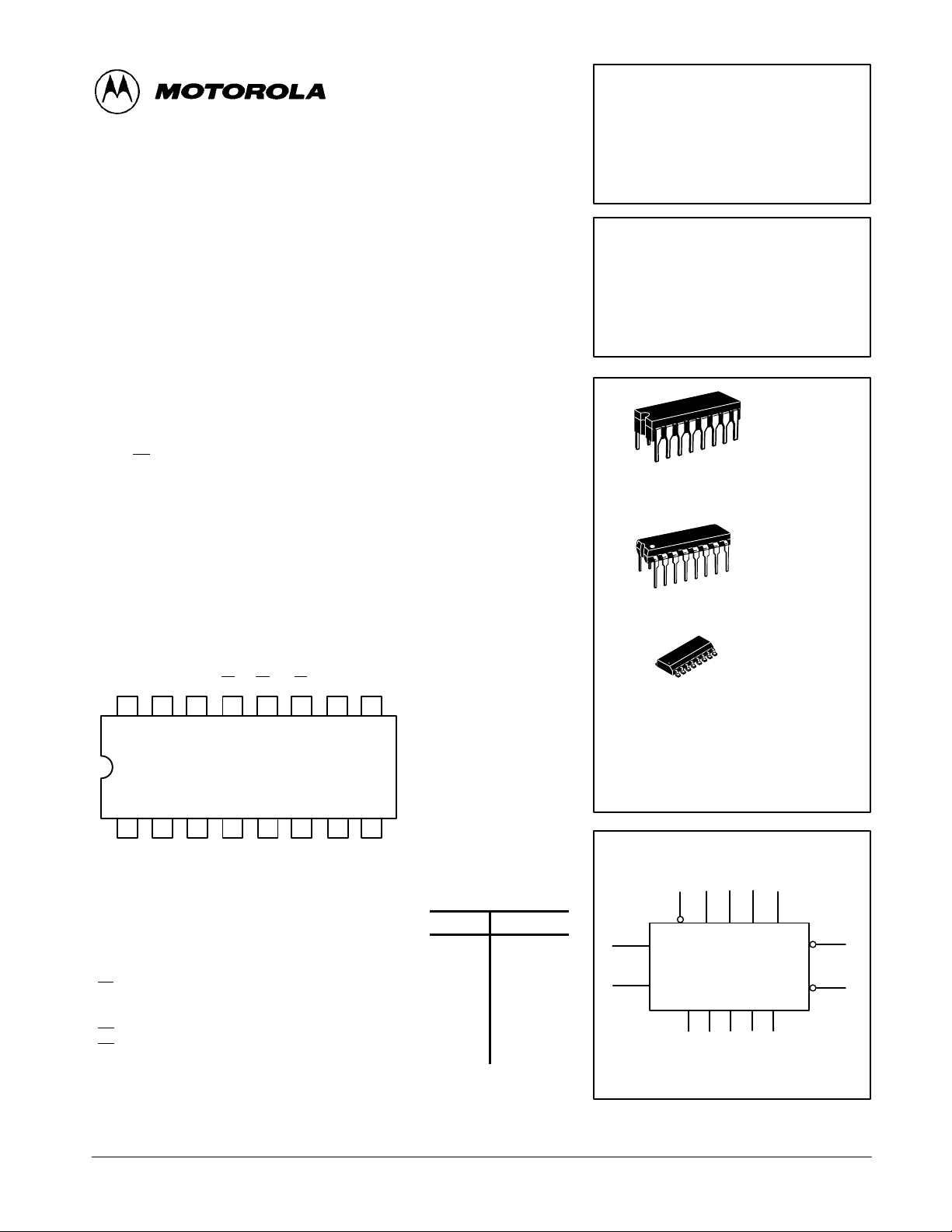
CONNECTION DIAGRAM DIP (TOP VIEW)
P
P
V
CC
16 15
P0MR TC
DTCU
14 13 12 11 10 9
PL
3
2
PRESETTABLE BCD/DECADE
UP/DOWN COUNTER
PRESETTABLE 4-BIT BINARY
UP/DOWN COUNTER
LOW POWER SCHOTTKY
J SUFFIX
CERAMIC
16
1
16
1
16
1
CASE 620-09
N SUFFIX
PLASTIC
CASE 648-08
D SUFFIX
SOIC
CASE 751B-03
NOTE:
The Flatpak version
has the same pinouts
(Connection Diagram) as
the Dual In-Line Package.
123456
Q1Q0CPDCPUQ2Q3GND
P
1
PIN NAMES LOADING (Note a)
CP
CP
MR
PL
P
n
Q
n
TC
TC
NOTES:
a. 1 TTL Unit Load (U.L.) = 40 µA HIGH/1.6 mA LOW.
b. The Output LOW drive factor is 2.5 U.L. for Military (54) and 5 U.L. for Commercial (74)
b. T emperature Ranges.
Count Up Clock Pulse Input
U
Count Down Clock Pulse Input
D
Asynchronous Master Reset (Clear) Input
Asynchronous Parallel Load (Active LOW) Input
Parallel Data Inputs
Flip-Flop Outputs (Note b)
Terminal Count Down (Borrow) Output (Note b)
D
Terminal Count Up (Carry) Output (Note b)
U
7
8
HIGH
0.5 U.L.
0.5 U.L.
0.5 U.L.
0.5 U.L.
0.5 U.L.
10 U.L.
10 U.L.
10 U.L.
LOW
0.25 U.L.
0.25 U.L.
0.25 U.L.
0.25 U.L.
0.25 U.L.
5 (2.5) U.L.
5 (2.5) U.L.
5 (2.5) U.L.
FAST AND LS TTL DAT A
5-1
ORDERING INFORMATION
SN54LSXXXJ Ceramic
SN74LSXXXN Plastic
SN74LSXXXD SOIC
LOGIC SYMBOL
PL
U
D
Q0Q1Q2Q
MR
14
0
326
VCC = PIN 16
GND = PIN 8
5
4
CP
CP
91011511
P
P2P1P
3
TC
TC
3
7
U
D
12
13
Page 2
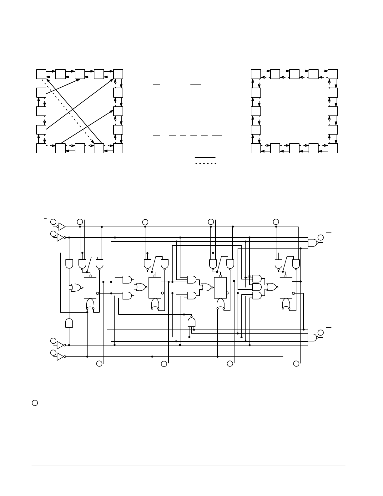
STATE DIAGRAMS
SN54/74LS192 • SN54/74LS193
0123
15
14
13
12
LS192
LOGIC DIAGRAMS
P
P
L
(LOAD)
CP
(UP COUNT)
U
5
15
4
LS192 LOGIC EQUATIONS
0123
4
FOR TERMINAL COUNT
5
6
U
TCD = Q0 ⋅ Q1 ⋅ Q2 ⋅ Q3 ⋅ CP
U
D
15
14
5
6
TC
= Q0 ⋅ Q3 ⋅ CP
LS193 LOGIC EQUATIONS
FOR TERMINAL COUNT
7
TCU = Q0 ⋅ Q1⋅ Q2⋅ Q3 ⋅ CP
TCD = Q0 ⋅ Q1 ⋅ Q2 ⋅ Q3 ⋅ CP
U
D
891011
COUNT UP
COUNT DOWN
0
P
1
1
P
2
10
13
12
7
891011
LS193
P
3
911
TC
12
U
(CARRY
OUTPUT)
CP
4
D
(DOWN
COUNT)
14
MR
(CLEAR)
VCC = PIN 16
GND = PIN 8
= PIN NUMBERS
S
D
Q
T
Q
C
D
3
Q
0
S
D
Q
T
Q
C
D
S
D
Q
T
Q
C
D
S
D
Q
T
Q
C
D
TC
13
D
(BORROW
OUTPUT)
2
Q
1
67
Q
2
Q
3
LS192
FAST AND LS TTL DATA
5-2
Page 3
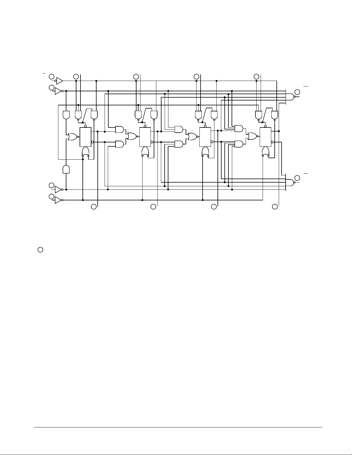
LOGIC DIAGRAMS (continued)
SN54/74LS192 • SN54/74LS193
P
L
(LOAD)
CP
(UP COUNT)
U
CP
D
(DOWN
COUNT)
MR
(CLEAR)
P
0
15
5
S
D
Q
T
Q
C
D
4
14
3
Q
0
P
1
1
P
2
10
P
3
911
TC
U
12
(CARRY
OUTPUT)
S
D
Q
T
Q
C
D
S
D
Q
T
Q
C
D
S
D
Q
T
Q
C
D
TC
13
D
(BORROW
OUTPUT)
2
Q
1
67
Q
2
Q
3
LS193
VCC = PIN 16
GND = PIN 8
= PIN NUMBERS
FAST AND LS TTL DATA
5-3
Page 4
SN54/74LS192 • SN54/74LS193
FUNCTIONAL DESCRIPTION
The LS192 and LS193 are Asynchronously Presettable
Decade and 4-Bit Binary Synchronous UP/ DOWN (Reversable) Counters. The operating modes of the LS192 decade
counter and the LS193 binary counter are identical, with the
only difference being the count sequences as noted in the
State Diagrams. Each circuit contains four master/slave
flip-flops, with internal gating and steering logic to provide
master reset, individual preset, count up and count down
operations.
Each flip-flop contains JK feedback from slave to master
such that a LOW-to-HIGH transition on its T input causes the
slave, and thus the Q output to change state. Synchronous
switching, as opposed to ripple counting, is achieved by
driving the steering gates of all stages from a common Count
Up line and a common Count Down line, thereby causing all
state changes to be initiated simultaneously . A LOW-to-HIGH
transition on the Count Up input will advance the count by one;
a similar transition on the Count Down input will decrease the
count by one. While counting with one clock input, the other
should be held HIGH. Otherwise, the circuit will either count by
twos or not at all, depending on the state of the first flip-flop,
which cannot toggle as long as either Clock input is LOW.
The Terminal Count Up (TC
(TC
) outputs are normally HIGH. When a circuit has reached
D
) and Terminal Count Down
U
the maximum count state (9 for the LS192, 15 for the LS193),
the next HIGH-to-LOW transition of the Count Up Clock will
cause TC
to go LOW. TCU will stay LOW until CPU goes
U
HIGH again, thus effectively repeating the Count Up Clock,
but delayed by two gate delays. Similarly , the TC
output will
D
go LOW when the circuit is in the zero state and the Count
Down Clock goes LOW. Since the TC outputs repeat the clock
waveforms, they can be used as the clock input signals to the
next higher order circuit in a multistage counter.
Each circuit has an asynchronous parallel load capability
permitting the counter to be preset. When the Parallel Load
) and the Master Reset (MR) inputs are LOW, information
(PL
present on the Parallel Data inputs (P0, P3) is loaded into the
counter and appears on the outputs regardless of the
conditions of the clock inputs. A HIGH signal on the Master
Reset input will disable the preset gates, override both Clock
inputs, and latch each Q output in the LOW state. If one of the
Clock inputs is LOW during and after a reset or load operation,
the next LOW-to-HIGH transition of that Clock will be
interpreted as a legitimate signal and will be counted.
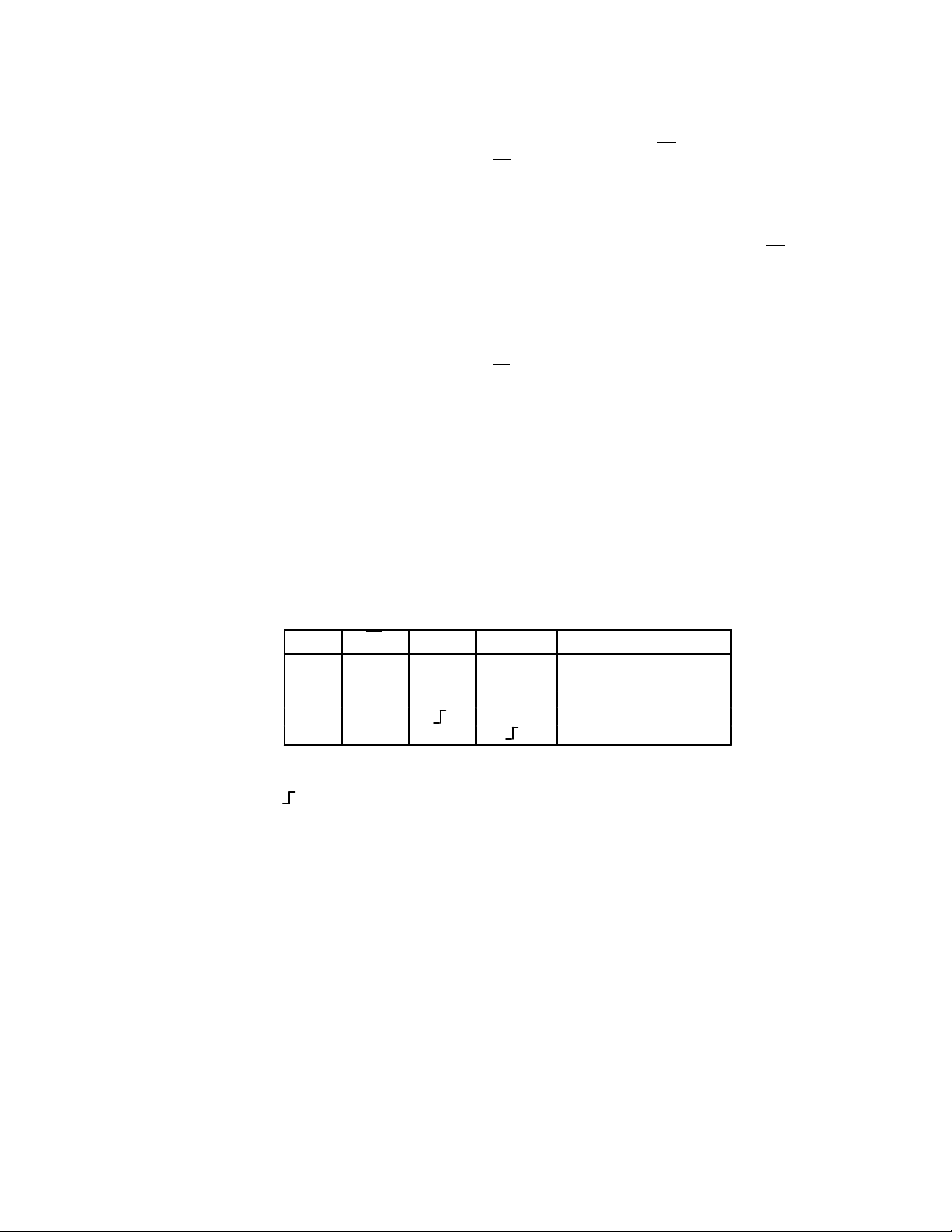
MODE SELECT TABLE
MR PL CP
H X X X Reset (Asyn.)
L L X X Preset (Asyn.)
L H H H No Change
L H H Count Up
L H H Count Down
L = LOW Voltage Level
H = HIGH Voltage Level
X = Don’t Care
= LOW-to-HIGH Clock Transition
U
CP
D
MODE
FAST AND LS TTL DATA
5-4
Page 5
SN54/74LS192 • SN54/74LS193
VILI
LOW Volt
V
pg
VOHOutput HIGH Volt
CC
,
OH
,
IN IH
VOLOutput LOW Volt
V
V
V
IIHI
HIGH C
t
CC
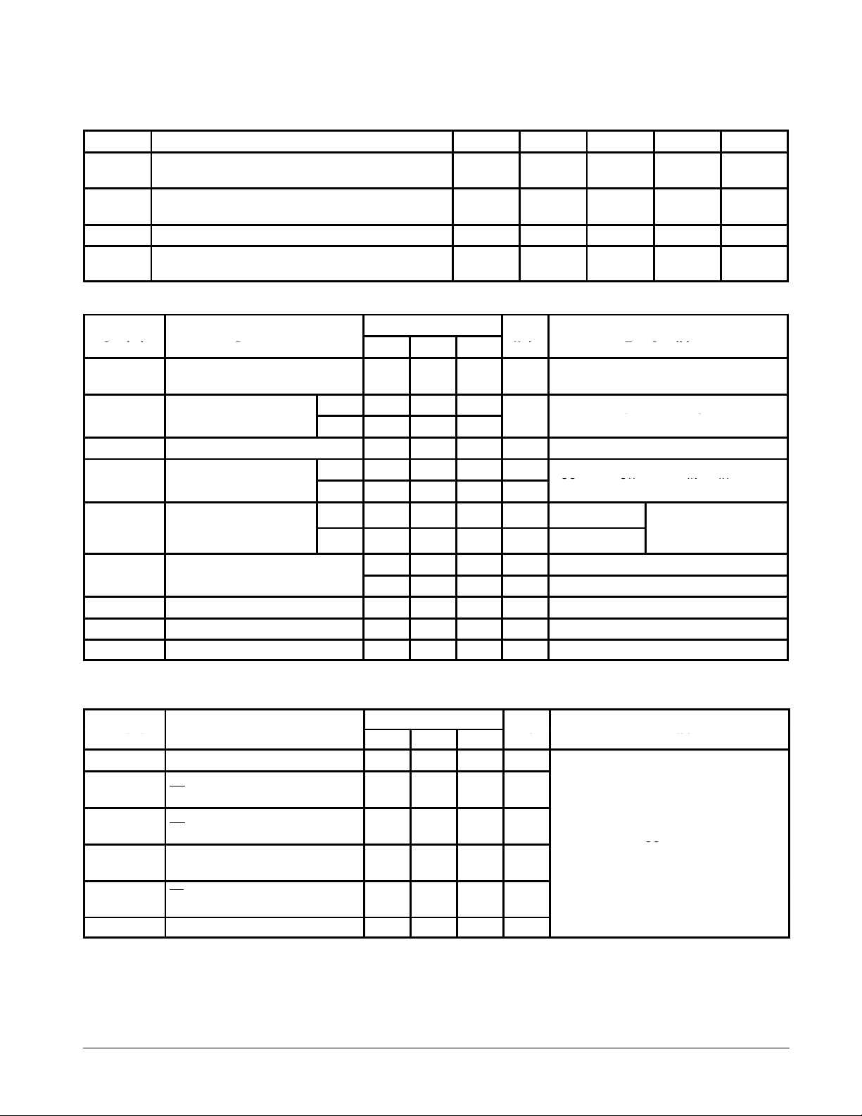
GUARANTEED OPERATING RANGES
Symbol Parameter Min Typ Max Unit
V
CC
T
A
I
OH
I
OL
DC CHARACTERISTICS OVER OPERATING TEMPERATURE RANGE (unless otherwise specified)
Symbol Parameter
V
IH
V
IK
I
IL
I
OS
I
CC
Note 1: Not more than one output should be shorted at a time, nor for more than 1 second.
Supply Voltage 54
Operating Ambient Temperature Range 54
Output Current — High 54, 74 –0.4 mA
Output Current — Low 54
Limits
Min Typ Max
Input HIGH Voltage 2.0 V
nput
Input Clamp Diode Voltage –0.65 –1.5 V VCC = MIN, IIN = –18 mA
nput
Input LOW Current –0.4 mA VCC = MAX, VIN = 0.4 V
Short Circuit Current (Note 1) –20 –100 mA VCC = MAX
Power Supply Current 34 mA VCC = MAX
age
age
age
urren
54 0.7
74 0.8
54 2.5 3.5 V
74 2.7 3.5 V
54, 74 0.25 0.4 V IOL = 4.0 mA
74 0.35 0.5 V IOL = 8.0 mA
74
74
74
20 µA VCC = MAX, VIN = 2.7 V
0.1 mA VCC = MAX, VIN = 7.0 V
4.5
4.75
–55
0
Unit Test Conditions
Guaranteed Input HIGH Voltage for
All Inputs
Guaranteed Input LOW Voltage for
All Inputs
VCC = MIN, IOH = MAX, VIN = V
or VIL per Truth Table
5.0
5.0
25
25
5.5
5.25
125
70
4.0
8.0
VCC = VCC MIN,
=
IN
IL
per Truth Table
or
IH
IH
V
°C
mA
AC CHARACTERISTICS (T
Symbol Parameter
f
MAX
t
PLH
t
PHL
t
PLH
t
PHL
t
PLH
t
PHL
t
PLH
t
PHL
t
PHL
Maximum Clock Frequency 25 32 MHz
CPU Input to
TC
Output
U
CPD Input to
TCD Output
Clock to Q
PL to Q
MR Input to Any Output 23 35 ns
A
= 25°C)
Limits
Min Typ Max
17
18
16
15
27
30
24
25
26
24
24
24
38
47
40
40
FAST AND LS TTL DATA
5-5
Unit Test Conditions
ns
ns
ns
ns
VCC = 5.0 V
CL = 15 pF
Page 6
SN54/74LS192 • SN54/74LS193
V
5.0 V
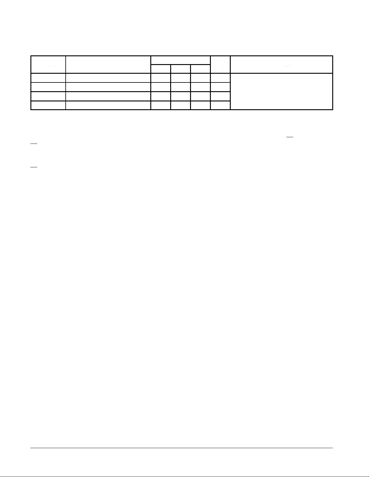
AC SETUP REQUIREMENTS (T
Symbol Parameter
t
t
t
t
W
s
h
rec
Any Pulse Width 20 ns
Data Setup Time 20 ns
Data Hold Time 5.0 ns
Recovery Time 40 ns
= 25°C)
A
Min Typ Max
DEFINITIONS OF TERMS
SETUP TIME (ts) is defined as the minimum time required for
the correct logic level to be present at the logic input prior to the
transition from LOW-to-HIGH in order to be recognized and
PL
transferred to the outputs.
HOLD TIME (th) is defined as the minimum time following the
transition from LOW-to-HIGH that the logic level must be
PL
maintained at the input in order to ensure continued recogni-
Limits
Unit Test Conditions
=
CC
tion. A negative HOLD TIME indicates that the correct logic
level may be released prior to the PL
transition from
LOW-to-HIGH and still be recognized.
RECOVERY TIME (t
) is defined as the minimum time
rec
required between the end of the reset pulse and the clock
transition from LOW-to-HIGH in order to recognize and
transfer HIGH data to the Q outputs.
FAST AND LS TTL DATA
5-6
Page 7
SN54/74LS192 • SN54/74LS193
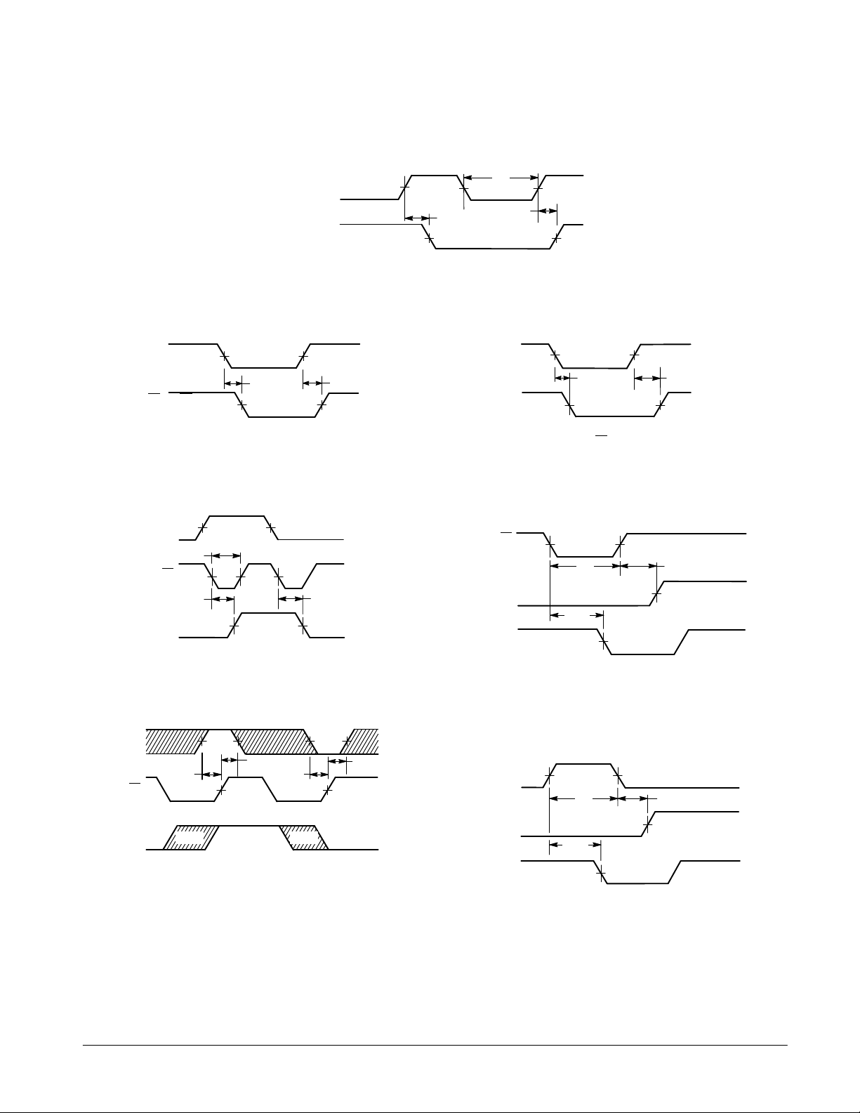
AC WAVEFORMS
t
CPU or CP
D
Q
1.3 V
t
PHL
1.3 V 1.3 V
Figure 1
W
t
PLH
1.3 V
CPU or CP
TC
P
n
PL
Q
n
D
t
PHL
or TC
U
D
Figure 2 Figure 3
t
w
1.3 V
t
PLH
1.3 V
1.3 V
P
PL
Q
n
n
Figure 4 Figure 5
1.3 V
t
t
s(H)
Q = P Q = P
h(H)
1.3 V
t
s(L)
1.3 V
t
PHL
1.3 V
t
PLH
1.3 V
t
h(L)
PL
CPU or CP
CPU or CP
D
MR
P
n
Q
n
Q
D
1.3 V
t
PHL
1.3 V
NOTE: PL = LOW
t
W
1.3 V
t
PHL
1.3 V
1.3 V
t
W
t
PHL
1.3 V
t
t
rec
t
rec
1.3 V
PLH
* The shaded areas indicate when the input is permitted
* to change for predictable output performance
Figure 6 Figure 7
FAST AND LS TTL DATA
5-7
Q
1.3 V
 Loading...