

Page 1
.
Electronic
Two-Tone Ringer
LS1240A
LOW CURRENT CONSUMPTION, IN ORDER
TO ALLOW THE P ARALLEL OPERATION O F 4
DEVICES
.
INTEGRATED RECTIFIER BRIDGE WITH
ZENER DIODES TO PROTECT AGAINST
OVERVOLTAGES
.
LITTLE EXTERNAL CIRCUITRY
.
TONE AND SWITC HING FREQUEN CIES ADJUSTABLE BY EXTERNAL COMPONENTS
.
INTEGRATED VOLTAGE AND CURRENT
HYSTERESIS
DESCRIPTION
LS1240A is a mon olith ic in tegrated circ uit de signed
to replace the mechanical bell in telephone sets in
connection with an electro-acoustical converter. It
can drive directly a piezoceramic converter (buzzer)or a dynam ic loudspe ak er .
The output current capability of LS1240A is higher
than standard ringer. For driving a dynamic loudspeaker LS 124 0A c an simply us e a dec oupling capacitor, thus elim inating the us ual trans f or m er .
No curre nt limitation is provided on the outpu t stage
of LS1240A, so a minimum load DC of 50 Ω is adviced, in s er ies with a proper c apac itor.
The two tone frequencies generated are switched
by an inte rnal oscillator in a fas t sequence and m ade
audible across an output amplifier in the loudspeaker, both tone frequencies and the switching
frequency c an be externally adj us t ed.
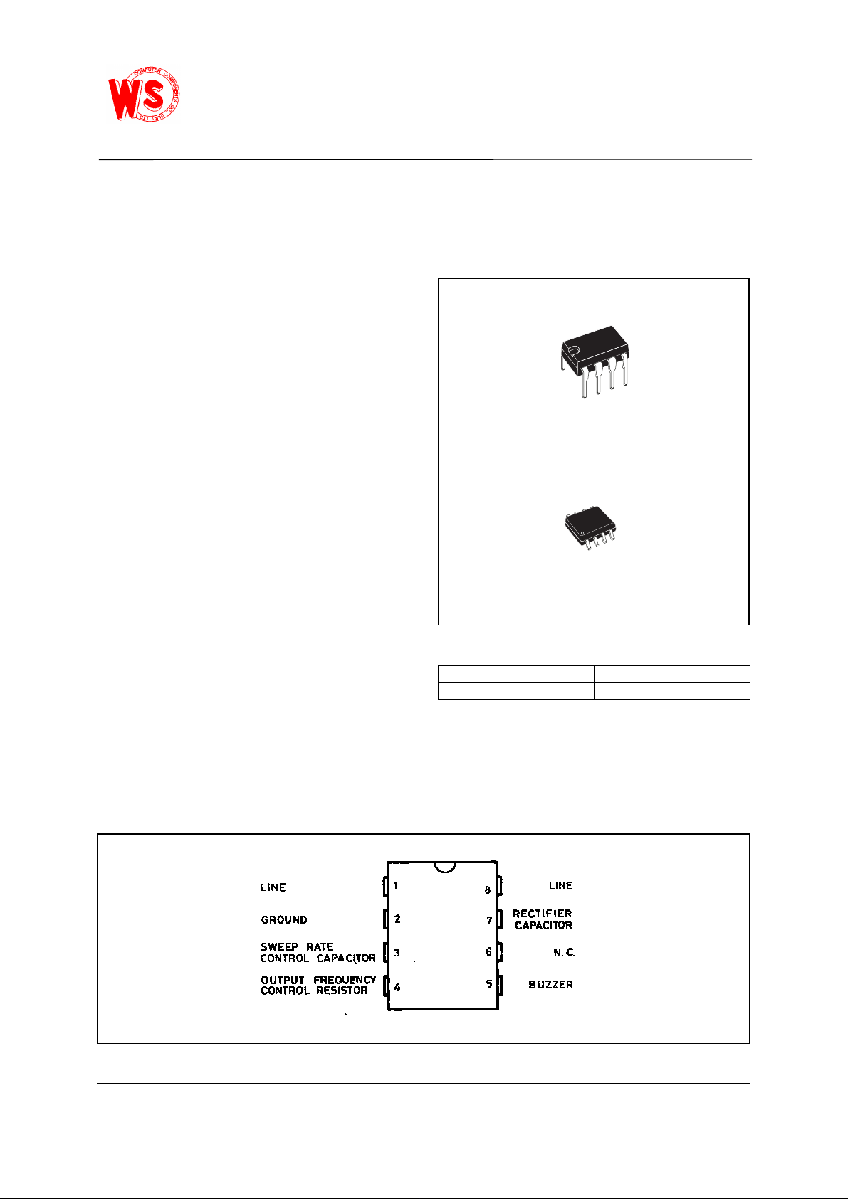
Minidip
SO8
ORDERING NUMBERS
Minidip SO8
LS1240A LS1240AD1
The suppl y voltage is obtained from the A C ring signal and the circuit is designed so that noise on the
line or variations of the ringing signal cannot affect
correct operation of the device.
PIN CONNECTION (top view)
Wing Shing Computer Components Co., (H.K.)Ltd. Tel:(852)2341 9276 Fax:(852)2797 8153
Homepage: http://www.wingshing.com E-mail: wsccltd@hkstar.com
Page 2
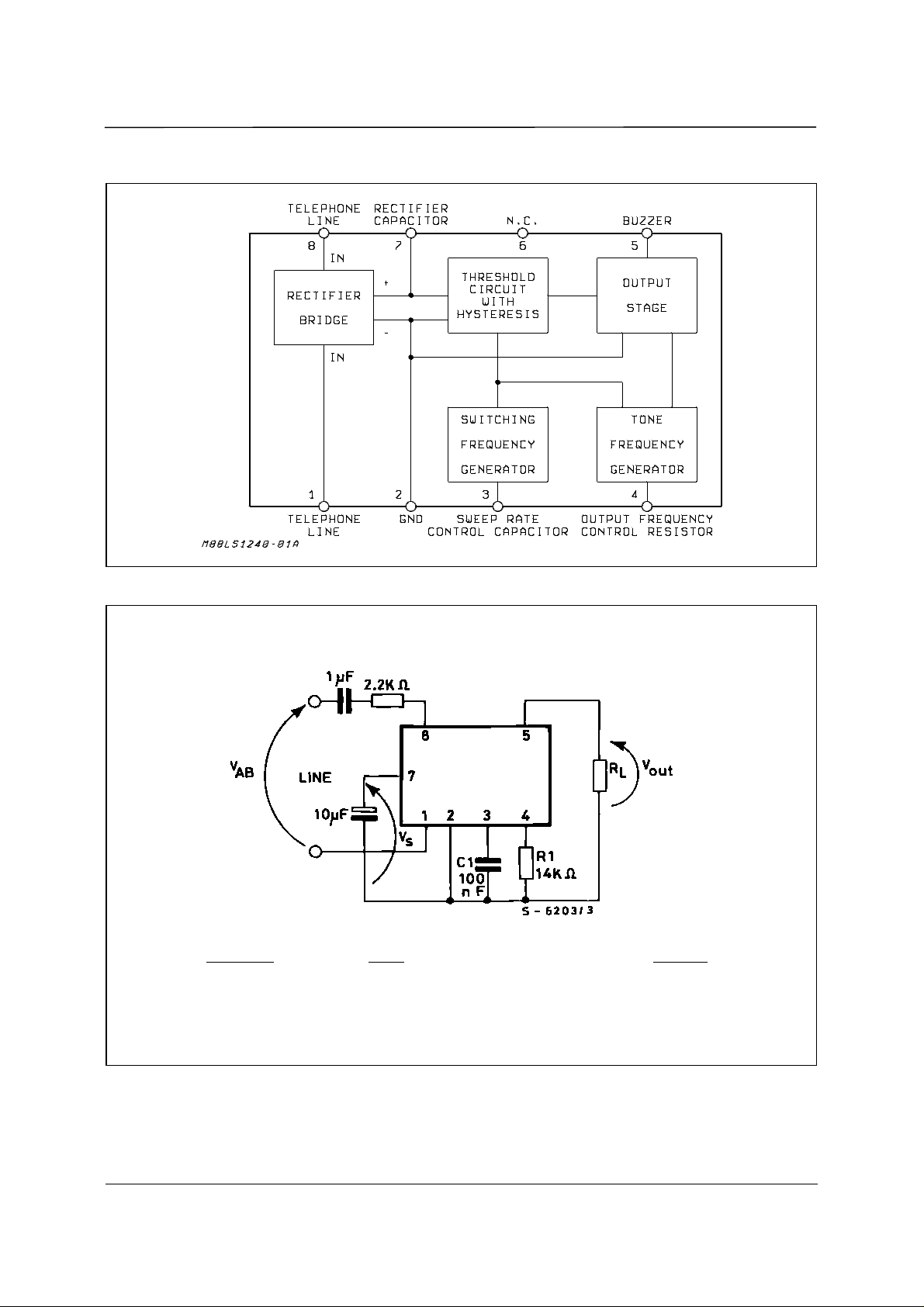
BLOCK DIAGRAM
WS
LS1240A
Figure 1 : Test Circuit.
2.72 ⋅ 10
R1 =
f1 (Hz)
4
⋅ (1 − 0.04 ln
f1
f2 = 0.725 f1 f
)
1943
SWEEP
=
C1 (nF)
750
Page 3

LS1240A
WS
2
12
13.5
V
9.3
V
7.8
1.55
2.53
1.08
1.9
2
ABSOLUTE MAXIMUM RATIN GS
Symbol Parameter Value Unit
V
AB
V
AB
DC Supply Current 30 mA
T
op
T
stg
THERMAL DATA
Symbol Parameter Value Unit
R
th j-amb
ELECTRICAL CHARACTERISTICS
= 25 °C; Vs = applied between pins 7-2 unless otherwise specified)
(T
amb
Symbol Parameter Test Conditions Min. Typ. Max. Unit
V
s
I
B
V
ON
V
OFF
R
D
V
OUT
I
OUT
AC OPERATION
f
1
f
2
f
SWEEP
Calling Voltage (f = 50 Hz) Continuous 120 V
Calling Voltage (f = 50 Hz) 5s ON/10s OFF 200 V
Operating Temperature– 0 to + 70
°
Storage and Junction Temperature – 65 to + 150
Thermal Resistance Junction-ambientMax00
C/W
°
Supply Voltage 26 V
Current Consumption without Load (pins 8-1) V
= 9.3 to 25 V 1.5 1.8 mA
8-1
Activation Voltage
Sustaining Voltage
Differential Resistance in OFF Condition (pins 8-1) 6.4
Output Voltage Swing Vs – 5 V
Short Circuit Current (pins 5-2)
Output Frequencies
f
out1
f
out2
f
OUT1
f
OUT2
V
= 20V RL = 250
s
Vs = 26V, R1 = 14k
Vs = 0 V
= 6V
V
s
Ω
Ω
1.33 1.43
70 mA
Programming Resistor Range 8 56
Sweep Frequency
R
= 14kΩ, C1 = 100nF
1
5.25 7.5 9.75 Hz
rms
rms
C
°
kHz
C
k
Ω
k
Ω
Page 4

Figure 2 : Typical Application wit h B UZZ E R
WS
LS1240A
Figure 3 : T y pic al Ap plic ation with Lou ds peak er (no trans for me r ne eded)
C1 such that Z
LOAD
> 1 ΚΩ
 Loading...