

Page 1
Data Sheet
LRS1338A-1
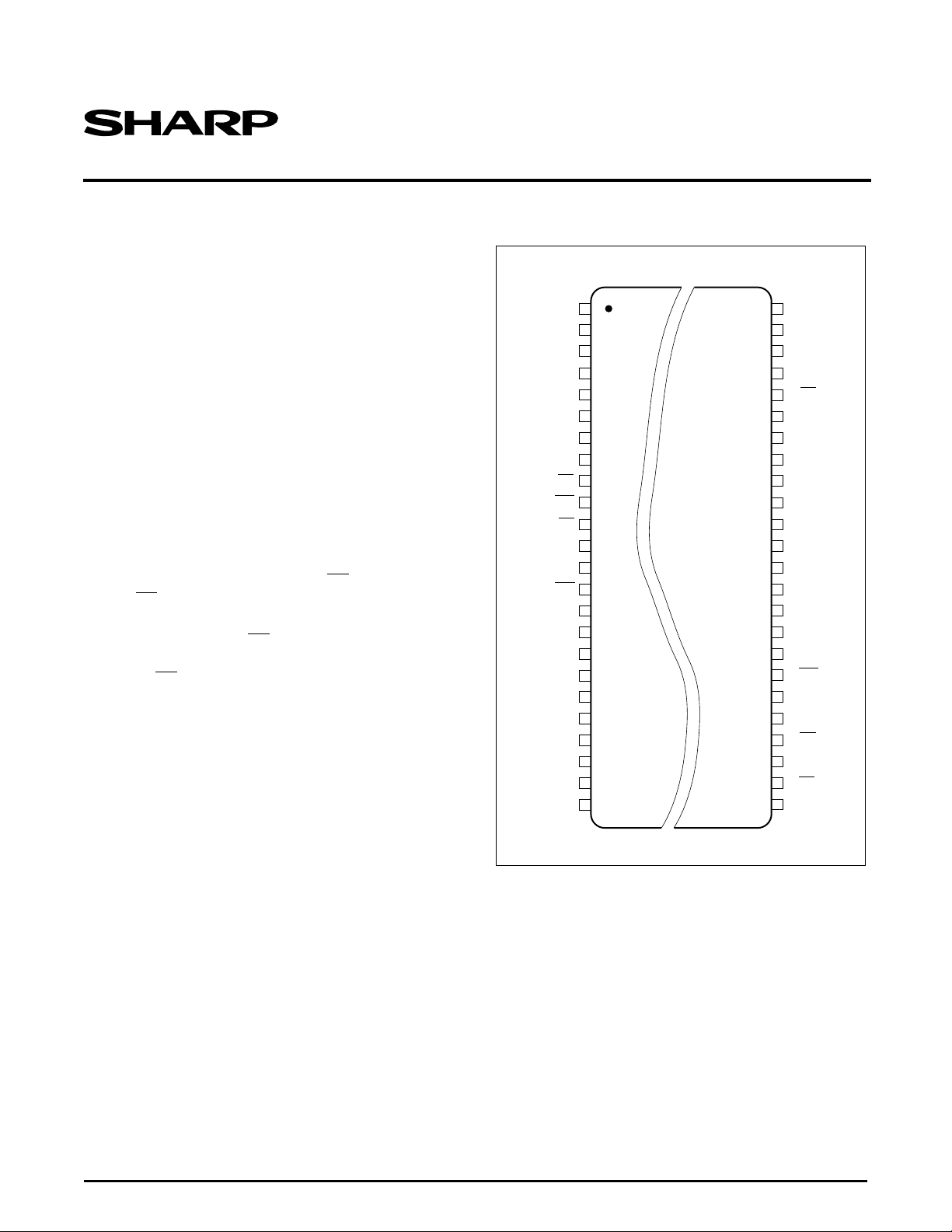
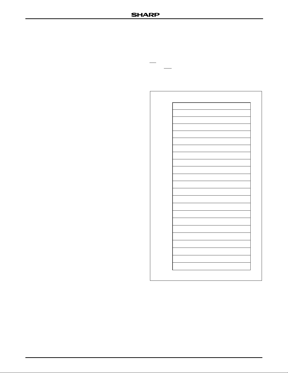
TOP VIEW48-PIN TSOP
2
3
4
5
8
9
S-A
9
/F-A
8
S-A12/F-A
11
S-A13/F-A
12
S-A14/F-A
13
48
45
42
6
7S-A
10
/F-A
9
S-A11/F-A
10
47
46
I/O
14
S-CE
I/O
15
I/O
13
10
11
12
I/O
7
13
44
I/O
3
43
I/O
10
I/O
6
14
15
16
17
18
19
20
39
36
41
40
38
37
I/O
1
S-WE
I/O
8
S-A7/F-A
6
S-A6/F-A
5
S-A8/F-A
7
F-A18
F-A17
F-WP
S-A
5
/F-A
4
I/O
0
F-OE
I/O
5
I/O
4
I/O
12
I/O
9
1
S-A
15
/F-A
14
S-A16/F-A
15
S-A17/F-A
16
21
22
23
24S-A
0
S-A2/F-A
1
S-A4/F-A
3
S-A3/F-A
2
34
F-CE
35
GND
31
33
32
30
29
S-A
1
/F-A
0
F-RP
F-WE
S-OE
F-V
PP
S-V
CC
F-V
CC
I/O
11
I/O
2
27
28
26
25
LRS1338A
Stacked Chip
8M Flash Memory and 2M SRAM
FEATURES
PIN CONFIGURATION
• Flash memory and SRAM
• Stacked die chip scale package
• 48-pin TSOP (TSOP48-P-1014) plastic package
• Power supply: 2.7 V to 3.6 V
• Operating temperature: -40°C to +85°C
• Access time (MAX.):
– Flash memory: 120 ns
– SRAM: 85 ns
• Operating current (MAX.):
–Flash memory
– Read: 25 mA (t
– Word write: 57 mA (F -V
– Block erase: 42 mA (F-V
– SRAM: 25 mA (t
• Standby current
2
CYCLE
CYCLE
= 200 ns)
≥ 3.0 V)
CC
≥ 3.0 V)
CC
= 200 ns)
– Flash memory: 20 µA MAX. (F-CE ≥ F-VCC - 0.2 V,
F-RP
≤ 0.2 V, F-VPP ≤ 0.2 V)
–SRAM:
– 40 µA MAX. (S-CE
• Fully static operation
• Three-state output
NOTES:
1. Block erase and word write operations of flash memory with
2. Total standby current is the summation of flash’s memory standby
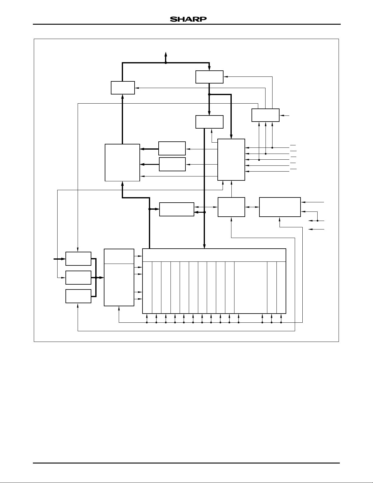
DESCRIPTION
as 524,288 × 16-bit flash memory and 262,144 × 8-bit
static RAM in one package. It is fabricated using silicongate CMOS process technology.
S-CE
< -30°C are not supported.
T
A
current and SRAM’s one.
The LRS1338A is a combination memory organized
≥ S-VCC - 0.2 V)
– 0.6 µA TYP. (T
A
≥ S-VCC - 0.2 V)
= 25°C, S-VCC = 3 V,
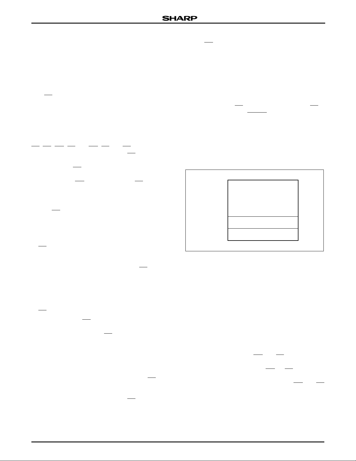
Figure 1. LRS1338A Pin Configuration
Data Sheet 1
Page 2
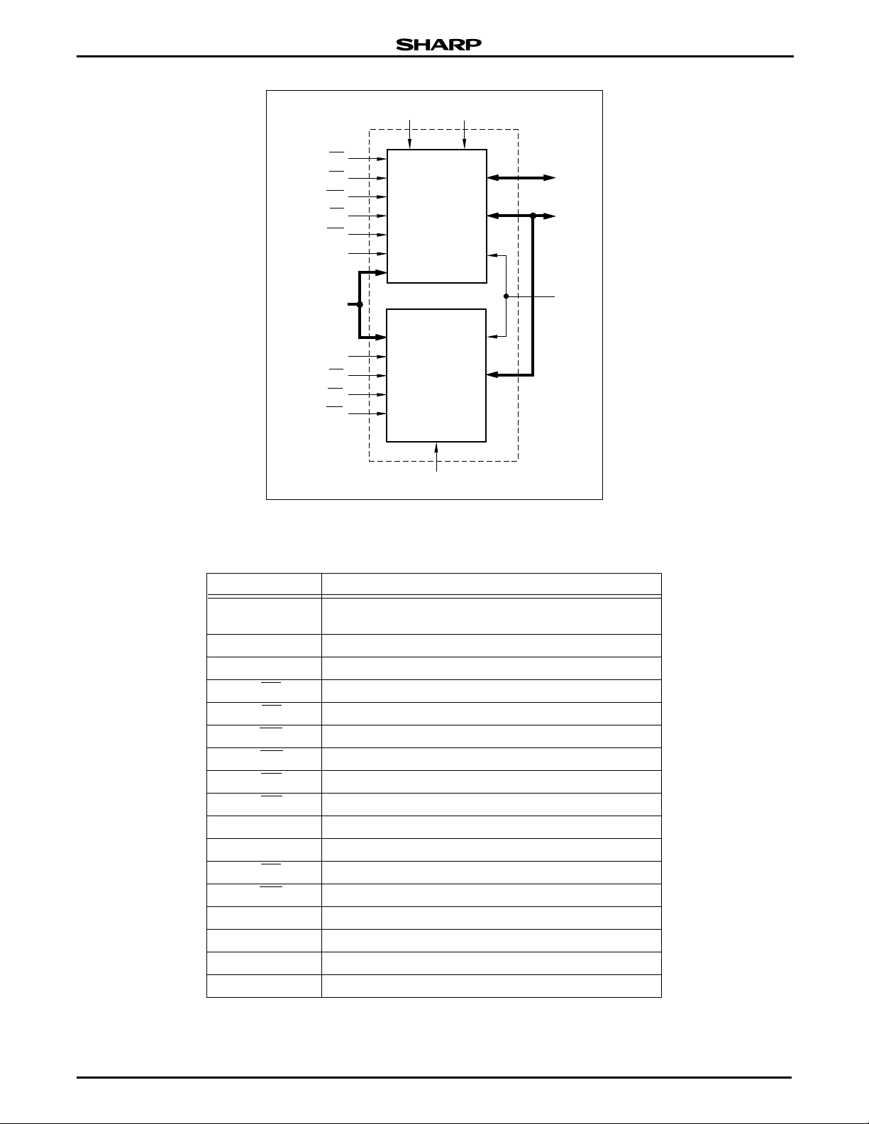
LRS1338A Stacked Chip (8M Flash & 2M SRAM)
CC
SRAM
S-V
F-V
CC
F-CE
F-OE
F-WE
F-RP
F-WP
, F-A
F-A
17
S-A1 to S-A
F-A
to F-A
0
S-A
S-CE
S-OE
S-WE
F-V
524,288 x 16 BIT
FLASH MEMORY
18
17
,
16
0
262,144 x 8 BIT
Figure 2. LRS1338A Block Diagram
PP
I/O8 to
I/O
15
I/O0 to
I/O
7
GND
LRS1338A-2
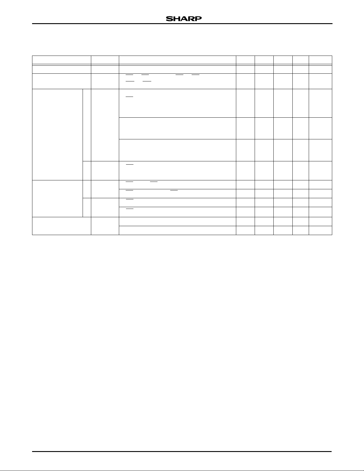
Table 1. Pin Descriptions
PIN DESCRIPTION
S-A
to S-A
1
F-A0 to F-A
S-A
F-A
17
F-CE
S-CE
F-WE
S-WE
F-OE
S-OE
I/O
0
I/O
to I/O
8
F-RP
F-WP
F-V
F-V
S-V
0
to F-A
to I/0
CC
PP
CC
17
Common Address Input Pins
16
Address Input Pin for SRAM
Address Input Pin for Flash Memory
18
Chip Enable Input Pin for Flash Memory
Chip Enable Input Pin for SRAM
Write Enable Input Pin for Flash Memory
Write Enable Input Pin for SRAM
Output Enable Input Pin for Flash Memory
Output Enable Input Pin for SRAM
Common Data Input/Output Pins
7
Data Input/Output Pins for Flash Memory
15
Reset/Deep Power Down Input Pin for Flash Memory
Write Protect Pin for Flash Memory’s Boot Block
Power Supply Pin for Flash Memory
Power Supply Pin for Flash Memory Write/Erase
Power Supply Pin for SRAM
GND Common Ground
2 Data Sheet
Page 3
Stacked Chip (8M Flash & 2M SRAM) LRS1338A
GENERAL DESIGN GUIDELINES
Supply Po wer
Maximum difference (between F-VCC and S-VCC) of
the voltage is less than 0.3 V.
Power Supply and Chip Enable of Flash
Memory and SRAM
It is forbidden that both F-CE and S-CE should be
LOW simultaneously. If the two memories are active
together, they many not op erate nor mally du e to inter ference noi ses or dat a collis ion on I/O bus. Bot h F-V
CC
and S-VCC need to be applied by the recommende d
supply voltage at the same time except SRAM data
retention mode.
SRAM Data Retention
SRAM data retention is capable in three ways.
SRAM power switching betwee n a system bat tery an d
a backup battery needs careful device decoupling from
Flash Memory to prevent SRAM supply voltage from
falling lower than 2.0 V by a Flash Mem ory peak current caused by transitio n of F la sh Mem or y supp ly vol tage or of control signals (F-CE
CASE 1: FLASH MEMORY IS IN STANDBY MODE
(F-V
= 2.7 V TO 3.6 V)
CC
• SRAM inputs and input/outputs except S-CE
be applied with voltages in the range of -0.3 V to
S-V
+ 0.3 V or to be open (HIGH-Z).
CC
• Flash Memory inputs and input/outputs except F-CE
and RP need to be applied with voltages in the range
of -0.3 V to S-V
+ 0.3 V or to be open (HIGH-Z).
CC
, F-OE, and RP).
need to
CASE 2: FLASH MEMORY IS IN DEEP POWER
DOWN MODE (F-V
• SRAM inputs and input/outputs except S-CE
= 2.7 V TO 3.6 V)
CC
need to
be applied with voltages in the range of -0.3 V to
S-V
+ 0.3 V or to be open.
CC
• Flash Memory inputs and input/outputs except RP
need to be applied with voltages in the range of -0.3 V
to S-V
be at the same level as F-V
+ 0.3 V or to be open (HIGH-Z). RP needs to
CC
or to be open.
CC
CASE 3: FLASH MEMORY POWER SUPPLY IS
TURNED OFF (F-V
• Fix RP
LOW level before tu rning off Flash memo ry
CC
= 0 V)
power supply.
• SRAM inputs and input/outputs except S-CE
need to
be applied with voltages in the range of -0.3 V to
S-V
+ 0.3 V or to be open (HIGH-Z).
CC
• Flash Memory inputs and input/outputs except RP
need to be applied with voltages in the range of
-0.3 V to S-V
+ 0.3 V or to be open (HIGH-Z).
CC
Power Up Sequence
When turning on Flash memory power supply, keep
RP
LOW. After F-VCC reaches ove r 2.7 V, keep RP
LOW for more than 100 ns.
Device Decoupling
The power supply needs to be designed c arefully
because one of the SRAM and the F lash Me mor y is in
standby mode when the other is active. A careful
decoupling of power supplies is necessary between
SRAM and Flash Memory. Note peak current caused
by transition of control signals (F-CE
, S-CE).
Table 2. Truth Table
F-CE F-OE F-WE F-RP S-CE S-OE S-WE ADDRESS MODE
L L H H H X X X Flas h read Output I
L H H H H X X X Flash read HIGH-Z I
LHLHHXX XFlash write Input I
H X X X L L H X SRAM read Output I
H X X X L H H X SRAM read HIGH-Z I
H X X X L X L X SRAM write Input I
H X X H H X X X Standby HIGH-Z I
X X X L H X X X Deep power down HIGH-Z I
NOTES:
1. F-CE
2. X can be V
3. Refer to DC Characteristics. When F-V
4. Do not use in a timing that both F-OE
should not be LOW when S-CE is LOW simultaneously.
or VIH for control pins and addresses, and V
for F-VPP. See DC Characteristics for V
tents can be read, but not altered.
IL
or V
and V
PPLK
≤ V
PP
and F-WE is LOW level.
PPLK
voltages.
PPH
, memory con-
PPLK
PPH
5. F-RP
6. Command writes involving block erase, write, or lock-bit configura-
7. Refer to Table 6 for valid D
1,2
to
I/O
0
I/O
at GND ± 0.2 V ensures the lowest deep power down current.
tion are reliably executed whe n F-V
block erase or word w rite operations wit h VIH < F-RP < VHH or
T
<-30°C produce spurious results and should not be attempted.
A
during a write operation.
IN
CURRENT NOTE
15
CC
CC
CC
CC
CC
CC
SB
SB
= V
PP
and F-VCC=V
PPH
3, 4
5
4, 6, 7
5
CC1
Data Sheet 3
Page 4
LRS1338A Stacked Chip (8M Flash & 2M SRAM)
ABSOLUTE MAXIMUM RATINGS
PARAMETER SYMBOL RATINGS UNIT NOTES
Supply voltage V
Input voltage V
Operating temperature T
Storage temperature T
voltage V
V
PP
CC
IN
OPR
STG
PP
Input voltage RP
NOTES:
1. The maximum applicable voltage on any pins with respect to GND.
2. Except V
3. Except RP
4. -2.0 V undershoot is allowed when the pulse width is less than 20 ns.
5. +14.0 V overshoot is allowed when the pulse width is less than 20 ns.
PP
.
.
-0.2 to +4.6 V 1, 2
-0.3 to VCC +0.3 V 1, 3, 4
-40 to +85 °C
-65 to +125 °C
-0.2 to +12.6 V 1, 5
-0.5 to +12.6 V 1, 4, 5
RECOMMENDED DC OPERATING CONDITIONS
TA = -40°C to +85°C
PARAMETER SYMBOL MIN. TYP. MAX. UNIT NOTES
Supply voltage V
Input voltage
CC
V
IH
V
IL
V
HH
2.7 3.0 3.6 V
2.0 VCC + 0.3 V 1
-0.3 0.8 V 2
11.4 12.6 3
NOTES:
1. V
is the lower one of S-VCC and F-VCC.
CC
2. -2.0 V undershoot is allowed when the pulse width is less than 20 ns.
3. This voltage is applicable to F-RP
pin only.
PIN CAPACITANCE
TA = 25°C, f = 1 MHz
PARAMETER SYMBOL CONDITION MIN. TYP. MAX. UNIT
Input capacitance* C
I/O capacitance* C
NOTE: *
Sampled by not 100% tested.
IN
I/O
VIN = 0 V 20 pF
V
= 0 V 22 pF
I/O
4 Data Sheet
Page 5
Stacked Chip (8M Flash & 2M SRAM) LRS1338A
DC ELECTRICAL CHARACTERISTICS
TA = -40°C to + 85°C, VCC = 2.7 V to 3.6 V
PARAMETER SYMBOL CONDITION MIN. TYP. MAX. UNIT NOTES
Input leakage current I
Output leakage current I
Operating supply
current
I
Flash
I
SRAM
I
Standby current
Flash
I
SRAM
Output voltage
NOTES:
1. This value is read current (I
2. Sampled but not 100% tested.
3. This value is operation current (I
4. This value is operation current (I
5. This value is operation current (I
VOL,
V
CCR
CC
CC
VIN = 0V to V
LI
F-CE, S-CE = VIH or F-OE, S-OE = VIH or
LO
, S-WE = VIH, V
F-WE
CC
= 0 V to V
I/O
CC
-1.5 1.5 µA
-1.5 1.5 µA
Read current, F-VPP ≤ F-VCC,
≤ 0.2 V, VIN ≥ VCC – 0.2 V or
F-CE
V
≤ 0.2 V
IN
= 200 ns, I
t
CYCLE
Summation of V
rent, and V
F-V
≥ 3.0 V
CC
PP
Summation of V
lock-bits current, and V
Block lock-bits current. F-V
= 0 mA
I/O
Byte Write or set l ock-bi t c ur-
CC
Byte Write or set lock-bit current.
Block Erase or Clear Block
CC
Block Erase or Clear
PP
≥ 3.0 V
CC
S-CE = 0.2 V, VIN ≥ VCC – 0.2 V or VIN ≥ 0.2 V
t
CYCLE
F-CE = VIH, RP = V
SB
F-CE
S-CE = V
SB
S-CE
= 200 ns, I
≥ VCC – 0.2 V, RP ≤ 0.2 V 20 µA 7
IH
≥ VCC – 0.2 V 0.6 40 µA 9, 10
= 0 mA
I/O
IH
IOL = 2.0 mA 0.4 V
I
OH
+ I
CCW
CCE
CC1
= 1.0 mA 2.4 V
OH
) of flash memory.
PPR
+ I
) of flash memory.
PPW
+ I
) of flash memory.
PPE
) of SRAM.
6. This value is standby current (I
7. This value is deep power down current (I
flash memory.
8. This value is standby current (I
9. This value is standby current (I
10.Reference values at V
CCS
SB1
SB
= 3.0 V and TA = +25°C
CC
25 mA 1
57 mA 2, 3
42 mA 2, 4
25 mA 5
2.0 mA 6
3.0 mA 8
+ I
) of flash memory.
PPS
CCD
) of SRAM
) of SRAM.
+ I
PPD
) of
Data Sheet 5
Page 6
LRS1338A Stacked Chip (8M Flash & 2M SRAM)
FLASH MEMORY*
New Features
The LRS1388A flash memory ma intain s backw ards
compatibility with SHARP’s LH28F 800B G- L.
• SmartVoltage technolog y
• Enhanced suspend capabilities
• Boot block architecture
Please note the following important differences:
• V
has been lowered to 1.5 V to support 3.0 V
PPLK
block erase and word write operations. Designs that
switch V
sure that the V
• Allow V
off during read ope rations should ma ke
PP
connection to 3.0 V.
PP
voltage transitions to GND.
PP
Product Overview
The LRS1338A is a high-performance 8M SmartVoltage flash memory organized as 512K-word of 16
bits. The 512K-word of data is arranged in two 4K-word
boot blocks, six 4K-word paramete r blocks and fifteen
32K-word main blocks wh ich are individuall y erasable
in-system. The memory map is shown in Figure 4.
SmartVoltage technolog y provides a choice of V
and VPP combinations, as shown in Table 3, to meet
system performance and power expectatio ns. In add ition to flexible erase and program voltages, the dedicated V
V
PP
≤ V
pin gives complete data protection when
PP
.
PPLK
Table 3. VCC and VPP Voltage Combinations
V
Voltage VPP Voltage
CC
2.7 V to 3.6 V 2.7 V to 3.6 V
Internal V
and VPP detection circuitry automati-
CC
cally configures the device for optimized read and write
operations.
CC
A Command User Interface (CUI) serves as the
interface between the system processor and internal
operation of the devi ce. A valid command seque nce
written to the CUI initiates device automation. An internal Write State Machine (WSM) automatically executes
the algorithms and timings necessary for block erase
and word write operations.
A block erase o perati on erases on e of the de vi ce’s
32K-word blocks typically within 1.14 se conds, 4Kword blocks typically with in 0 .38 s ec on ds ind epe nden t
of other blocks. Each block can be independently
erased 100,000 times. Block erase suspend mode
allows system software to suspend block erase to read
or write data from any other block.
Writing memory data is performed in word increments
of the device’s 32K-word blocks typically within 44.6 µs,
4K-word blocks typically within 45.9 µs. Word write suspend mode enables the system to read data or execute
code from any other fl as h me mor y array location.
The boot blocks can be locked for the WP
pin. Block
erase or word write fo r boot b lock mus t not be car ried
out by WP
to LOW and RP to VIH.
The status register indicates when the WSM’s block
erase or word write operation is finished.
The access time is 120 ns (t
cial temperature range (-40°C to +85°C) and V
) over the commer-
AVQV
CC
sup-
ply voltage range of 2.7 V to 3.6 V.
The Automatic Power Savi ngs (APS) feature substantially reduces activ e current when the devic e is in
static mode (addresses not switching). In APS mode,
the typical I
When CE
standby mode is enabled. When the RP
current is 1 mA at 3.3 V VCC.
CCR
and RP pins are at VCC, the ICC CMOS
pin is at GND,
deep power-down mode is enabled which minimi zes
power consumption a nd provide s write pr otection during reset. A reset time (t
) is required from RP
PHQV
switching HIGH until output s are valid. Likewise, the
device has a wake time (t
writes to the CUI are recognized. With RP
) from RP HIGH until
PHEL
at GND, the
WSM is reset and the status register is cleared.
NOTE: *
mands, voltage, etc. refer only to the Flash portion of this chip.
In the Flash Me mory sectio n all referenc e to pins, com -
6 Data Sheet
Page 7
Stacked Chip (8M Flash & 2M SRAM) LRS1338A
- I/O
I/O
0
15
INPUT
BUFFER
OUTPUT
BUFFER
A0 - A
I/O
15
BLOCKS
LOGIC
PROGRAM/ERASE
VOLTAGE
SWITCH
DATA
REGISTER
IDENTIFIER
REGISTER
OUTPUT
MULTIPLEXER
18
INPUT
BUFFER
ADDRESS
LATCH
ADDRESS
COUNTER
Y
DECODER
X
DECODER
. . .
STATUS
REGISTER
DATA
COMPARATOR
BOOT BLOCK 0
BOOT BLOCK 1
PARAMETER BLOCK 0
PARAMETER BLOCK 1
PARAMETER BLOCK 2
PARAMETER BLOCK 3
COMMAND
USER
REGISTER
WRITE
STATE
MACHINE
Y GATING
32K-WORD
MAIN BLOCK 0
MAIN BLOCK 1
PARAMETER BLOCK 4
PARAMETER BLOCK 5
V
CC
CE
WE
OE
RP
WP
MAIN BLOCK 13
MAIN BLOCK 14
V
PP
V
CC
GND
. . .
LRS1338A-3
Figure 3. Flash Memory Block Diagram
Data Sheet 7
Page 8
LRS1338A Stacked Chip (8M Flash & 2M SRAM)
Table 4. Flash Pin Descriptions
SYMBOL TYPE NAME AND FUNCTION
A
0
- A
18
Input
ADDRESS INPUTS: Inputs for addresses during read and write operations.
Addresses are internally latched during the write cycle.
DATA INPUT/OUTPUTS: Inputs da ta an d co mman ds du ring C UI wr ite cycl es ; ou t-
I/O
- I/O
0
15
Input/Output
puts data during memory array, status register, and identifier code read cycles. Data
pins float to HIG H- imp edan ce wh en the chi p is dese le ct ed or ou tp uts a r e di sabl e d.
Data is internally la tc he d dur in g a writ e cycle .
CHIP ENABLE: Activates the device’s control logic, input buffers, decoders, and
CE
Input
sense amplifiers. CE-HIGH deselects the device and reduces power consumption
to standby levels.
RESET/DEEP POWER-DOWN: Puts the device in deep power-down mode and
RP
Input
resets internal automation. RP
LOW, RP
inhibits write operations which provides data protection during power
transitions. Exit from deep power-down sets the device to read array mode. With
RP
= VHH, block erase or word write can operate to all blocks without WP state.
Block erase or word write with V
-HIGH enables normal operation. When driven
IH
not be attempted.
OE
WE
WP
Input OUTPUT ENABLE: Gates the device’s outputs during a read cycle.
Input
Input
WRITE ENABLE: Controls writes to the CIU and array blocks. Addresses and data
are latched on the rising edge of the WE
WRITE PROTECT: Master control for boot blocks locking. When V
blocks cannot be erased and programmed.
BLOCK ERASE an d WORD WRITE P OWER SUPPLY: For erasin g array bloc ks or
V
PP
Supply
writing words. With V
and word write with an invalid V
PP
≤ V
, memory contents cannot be altered. Block erase
PPLK
PP
results and should not be attempted.
DEVICE POWER SUPPLY: Do not float any power pins. With V
V
CC
Supply
write attempts to the flash memory are inhibited. Device operations at invalid
V
voltage (see ‘DC Characteristics’) produce spurious results and should not
CC
be attempted.
GND Supply GROUND: Do not float any ground pins.
< RP < VHH produce spurious results and should
pulse.
, locked boot
IL
(see ‘DC Characteristics’) produce spurious
CC
≤ V
LKO
, all
8 Data Sheet
Page 9
Stacked Chip (8M Flash & 2M SRAM) LRS1338A
7
7F000
7FFFF
7EFFF
FE000
7DFFF
7D000
7CFFF
7C000
7BFFF
7B000
7AFFF
7A000
79FFF
79000
78FFF
78000
77FFF
70000
6FFFF
68000
67FFF
58000
57FFF
60000
5FFFF
50000
4FFFF
48000
47FFF
40000
3FFFF
38000
37FFF
30000
2FFFF
28000
27FFF
20000
1FFFF
18000
17FFF
10000
0FFFF
08000
07FFF
00000
8
9
10
11
12
13
14
32K-WORD MAIN BLOCK
632K-WORD MAIN BLOCK
532K-WORD MAIN BLOCK
4 32K-WORD MAIN BLOCK
332K-WORD MAIN BLOCK
232K-WORD MAIN BLOCK
132K-WORD MAIN BLOCK
032K-WORD MAIN BLOCK
54K-WORD PARAMETER BLOCK
44K-WORD PARAMETER BLOCK
34K-WORD PARAMETER BLOCK
24K-WORD PARAMETER BLOCK
14K-WORD PARAMETER BLOCK
04K-WORD PARAMETER BLOCK
14K-WORD BOOT BLOCK
0
4K-WORD BOOT BLOCK
TOP BOOT
32K-WORD MAIN BLOCK
32K-WORD MAIN BLOCK
32K-WORD MAIN BLOCK
32K-WORD MAIN BLOCK
32K-WORD MAIN BLOCK
32K-WORD MAIN BLOCK
32K-WORD MAIN BLOCK
LRS1338A-4
Principles of Operation
The LRS1388A SmartVoltage flash memory
includes an on-chip W SM to manage bloc k erase and
word write functions. It allows for: 100% TTL-level control inputs, fixed power supplies during block erasure,
word write, and minimal processor overhead with
RAM-like interface timings.
After initial device power-up or return from deep
power-down mode (see ‘Bus Operatio n’), the device
When V
altered. The CUI, with two-step bloc k erase or word
write command sequences, provides protec tion from
unwanted operations even when high voltage is
applied to V
V
is below the write lockout voltage V
CC
RP
is at VIL. The device’s boot blocks locking capability for WP
vertent code or data alteration by block erase and
word write operations.
≤ V
PP
. All write functions are d isabled when
PP
, memory contents cannot be
PPLK
provides additional protection from inad-
defaults to re ad array mode . Manipulation of external
memory control pins allow array read, standby, and
output disable operations.
Status register and identifier codes can be accessed
through the CUI indep endent of the F-V
High voltage on F-V
enables successful block era-
PP
voltage.
PP
sure and word writing. All functions associated with
altering m emory co ntents — block erase, word write,
status, and identifier codes — are accessed via the CUI
and verified through the status register.
Commands are written using standard microprocessor write timings. The CUI contents serve as input to
the WSM, which controls the block erase and word
write. The internal algorithms are regulated by the
WSM including pulse repetition , internal verif ication,
and margining of d ata. Addresses a nd data are internally latched during write cycles. Wr iting the appropriate command outputs array data, accesses the
identifier codes or outputs status register data.
Interface software that initiates and polls progress of
block erase and word write can be stored in any block.
This code is copied to and executed from system RAM
during flash memory updates. After successful completion, reads are again possible via the Read Array command. Block erase suspend allows system software to
suspend a block erase to read/write dat a from/to blocks
other than that which is suspended. Word writ e suspend allows system software to suspend a word write to
read data from any other flash memory array location.
DATA PROTECTION
Depending on the appl ication, the syst em designer
may choose to make the V
(available only when memor y block erases or word
writes are required) or hardwir ed to V
accommodates either design practice and encourages
optimization of the processor-memory interface.
Data Sheet 9
power supply switchable
PP
. The device
PPH
Figure 4. Memory Map
LKO
or when
Page 10
LRS1338A Stacked Chip (8M Flash & 2M SRAM)
RESERVED FOR
FUTURE IMPLEMENTATION
DEVICE CODE
MANUFACTURER CODE
7FFFF
00001
00000
1338A-5
Bus Operation
The local CPU reads and writes f lash memory insystem. All bus cycles to or from the flash memory conform to standard microprocessor bus cycles.
READ
Information can be read from any block, identifier
codes or status register independent of the V
age. RP
can be either VIH or VHH.
The first task is to write the appropriate read mode
command (Read Array, Read Identifier Codes, or Read
Status Register) to the CUI. Upon initial device powerup or after exit from deep power-down mode, the device
automatically resets to read array mode. Five control
pins dictate the data flow in and out of the component:
CE
, OE, WE, RP and WP. CE and OE must be drive n
active to obtain data at the outputs. CE
is the device
selection control, and when active enables the selected
memory device. OE
is the data output (I/O0 - I/O15) control and when active drives the selected memory data
onto the I/O bus. WE
V
or VHH. Figure 12 illustrates a read cycle.
IH
must be at VIH and RP must be at
OUTPUT DISABLE
With OE
puts are disabled. Output pins (I/O
at a logic-HI GH le ve l ( VIH), the device out-
- I/O15) are placed
0
in a HIGH impedance state.
PP
volt-
As with any automated device, it is important to
assert RP
during system reset. When the system
comes out of reset, i t ex pec ts to re ad f ro m fl ash m emory. Automated flash memories provide status information when accessed during block erase or word write
modes. If a CPU reset occur s with no flash memory
reset, proper CPU initialization may not occur because
the flash memory may be provid ing status in formation
instead of arr ay data. SHARP ’s flash memories allow
proper CPU initialization following a system reset
through the use of RP
controlled by the same RESET
input. In this appl ication, RP is
signal that resets the
system CPU.
READ IDENTIFIER CODES OPERATION
The read identifier codes operation outputs the manufacturer code and devic e codes, the system CP U can
automatically match the device with its proper algorithms.
STANDBY
CE
at a logic HIGH level (VIH) places the device in
standby mode which substantially reduces device
power consumption. I/O
a HIGH-impedance st ate independent of OE
- I/O15 outputs are placed in
0
. If deselected during block erase or word write, the device continues functioning, and consuming active power until
the operation completes.
DEEP POWER-DOWN
RP
at VIL initiates the deep power down mode.
In read modes, RP
-LOW deselects the memory,
places output driver s in a HIGH-impedance s tate and
turns off all internal circuits. RP
a minimum of 1 00 ns. Time t
must be held LOW for
is required after
PHQV
return from power-down until initial memory access
outputs are valid. After this wake-up interval, normal
operation is restored. The CUI is reset to read array
mode and status register is set to 80H.
During block erase or word write modes, RP
-LOW
will abort the operation. Memory contents being altered
are no longer valid; the data may be partially erased or
written. Time t
HIGH (V
) before another command can be written.
IH
is required after RP goes to logic
PHWL
Figure 5. Device Identifier Code Memory Map
WRITE
Writing commands to the CUI enable reading of
device data and identifier codes. T hey also control
inspection and clearing of the status register.
When V
CC
= V
and VPP = V
CC1
, the CUI add i-
PPH
tionally controls block erasure and word write. The
Block Erase comman d requ ires ap propr iate com man d
data and an address within the block to be erased. The
Word Write command requires the command and
address of the location to be written.
The CUI does not occupy an addressable memory
location. It is wri tten wh en WE
and CE are active. The
address and data needed to execute a command ar e
latched on the rising edge of WE
or CE (whichever
goes HIGH first). Standard microprocessor write timings are used. F igure 13 a nd 14 illustrat e WE
and CE
controlled write operations.
10 Data Sheet
Page 11
Stacked Chip (8M Flash & 2M SRAM) LRS1338A
COMMAND DEFINITIONS
When VPP ≤ V
, Read oper ation s from t he statu s
PPLK
Device operations are selected by writ ing specific com-
mands into the CUI. Tabl e 6 defines these comma nds.
register, identifier codes or blocks are enabled. Placing
V
on VPP enables successful block erase and word
PPH
write operations.
Table 5. Bus Operations
MODE RP
Read V
Output Disable V
Standby V
Deep Power-Down V
Read Identifier Codes V
Write V
NOTES:
1. Refer to ‘DC Characteristics’. When V
2. X can be V
See ‘DC Characteristics’ for V
3. Never hold OE
at GND ± 0.2 V ensures the lowest deep power-down current.
4. RP
5. See ‘Read Identifier Codes Command’ for read identifier code data.
6. Command writes involving block erase or word write are reliably executed when V
Block erase or word write with V
7. Refer to Table 6 for valid D
or VIH for control pins and addresses, and V
IL
LOW and WE LOW at the same time.
or V
IH
HH
or V
IH
HH
or V
IH
HH
IL
or V
IH
HH
or V
IH
HH
PP
and V
PPLK
< RP < VHH produce spurious results and should not be attempted.
IH
during a write operations.
IN
CE OE WE ADDRESS V
V
IL
V
IL
V
IH
V
IL
V
IH
V
IH
V
IH
XX X XHIGH Z
XXX X XHIGH Z4
≤ V
PPH
V
IL
V
IL
, memory contents can be read, but not altered.
PPLK
voltages.
V
V
PPLK
IL
IH
or V
PPH
V
IH
V
IL
for VPP.
I/O0 - I/O15NOTES
PP
XXD
OUT
1, 2, 3
XXHIGH Z
See Figure 3 X 5
XXDIN3, 6, 7
= V
PP
and VCC = V
PPH
CC1
.
1
4
OPER.2ADDR.3DATA
4
NOTES
COMMAND
Read Array/Reset
Read Identifier Codes
Table 6. Command Definitions
BUS CYCLES
REQUIRED
FIRST BUS CYCLE SECOND BUS CYCLE
OPER.
2
ADDR.
3
DATA
1 Write X FFH
2 Write X 90H Read IA ID 5
≥
Read Status Register 2 Write X 70H Read X SRD
Clear Status Register 1 Write X 50H
Block Erase 2 Write BA 20H Write BA D0H 6
Word Write 2 Write WA 40H or 10H Write WA WD 6, 7
Block Erase and Word
Write Suspend
Block Erase and Word
Write Resume
NOTES:
1. Commands other than those shown in table are reserved by SHARP for
future device implementations and should not be used.
2. BUS operations are defined in Table 5.
3. X = Any valid address within the device; IA = Identifier Code Address, see Figure 5.
BA = Address within the block being erased; WA = Address of memory location to be written.
4. SRD = Data read from status register. See Table 9 for a description of the status register bits.
WD = Data to be written at location WA. Data is latched on the rising edge of WE
ID = Data read from identifier codes.
5. Following the Read Identifier Codes command, read operations access manufacturer and device codes.
See ‘Read Identifier Codes Command’ for read identifier code data.
6. When WP
Attempts to issue a block erase or word write to a locked boot block while RP
7. Either 40H or 10H are recognized by the WSM as the word write setup.
= VIL, RP must beat VHH to enable block erase or word write operations.
1WriteXB0H 6
1WriteXD0H 6
or CE (whichever goes HIGH first).
= VIH.
Data Sheet 11
Page 12

LRS1338A Stacked Chip (8M Flash & 2M SRAM)
READ ARRAY COMMAND
Upon initial device power-up and after exit from
deep power-down mode, the device defaults to read
array mode. This operation is also initiated by writing
the Read Array command. The device remains
enabled for reads until another command is written.
Once the internal WSM has started a block erase or
word write, the device will not recognize the Read Array
command until the WSM completes its operatio n
unless the WSM is suspended via an Erase Sus pend
or Word Write Suspend command. The Read Array
command functions ind ependently of V
RP
can be VIH or VHH.
voltage and
PP
READ IDENTIFIER CODES COMMAND
The identifier code operation is initiated by writing the
Read Identifier Codes command. Following the command write, read cycles from addresses shown in Figure 5 retrieve the manufacturer and device codes (see
Table 7 for identifier code values). To terminate the
operation, write another valid command. Like the Read
Array command, the Read Id entifier Codes command
functions independently of the V
be V
or VHH. Following the Read Identifier Codes
IH
voltage and RP can
PP
command, the following information can be read.
Table 7. Identifier Codes
CODE ADDRESS DATA
Manufacture Code 00000H 00B0H
Device Code (Top Boot) 00001H 0060H
READ STATUS REGISTER COMMAND
The status register may be r ead to d eterm ine whe n
a block erase or word write is complete and whether
the operation completed successfully. It may be read at
any time by writi ng the Read Status Register command. After writing this command, all subsequent read
operations output data from the status register until
another valid com mand is written. T he status regi ster
contents are latche d on the falling edge of OE
whichever occurs. OE
or CE must toggle to VIH before
or CE,
further reads to update the status register latch. The
Read Status Register command func tions independently of the V
voltage. RP can be VIH or VHH.
PP
CLEAR STATUS REGISTER COMMAND
Status register bits SR.5, SR.4, SR.3 or SR.1 are set
to ‘1’s by the WSM a nd c an on ly be r es et by the Clear
Status Register comma nd. The se bits in dicate various
failure conditions (see Table x). By allowing system
software to re set these bits , several ope rations (suc h
as cumulativel y erasi ng multi ple bloc ks or w riting several words in sequence) may be performed. The status
register may be polled to determine if an error occurred
during the sequence.
To clear the status regis te r, the Cl ear S tatu s Regi ster command (50H) is written. It functio ns independently of the applied V
V
. This command is not functional during block
HH
voltage. RP can be VIH or
PP
erase or word write suspend modes.
BLOCK ERASE COMMAND
Erase is executed one block at a time an d initiated
by a two-cycle command. A block erase setup is first
written, followed by a block erase confirm. This command sequence requires appropriate sequencing an d
an address within the block to be erased (erase
changes all block data to FFFFH). Bloc k precondi tioning, erase, an d verify are handle d internally by th e
WSM (invisible to the system). After the two-cycle block
erase sequence is written, the device automatically
outputs status register data when read (see Figure 6) .
The CPU can detect block erase completion by analyzing the output data of the status register bit SR.7.
When the block erase is complete, status register bit
SR.5 should be checked. If a block erase error is
detected, the status regi ster should be cleare d before
system software attempts corrective action. The CUI
remains in read s tatus registe r mod e unti l a new command is issued.
This two-step command sequence of set-up followed by execution ensures that block contents are not
accidentally eras ed. An inva lid Block Er ase comman d
sequence will result in both status reg ister bits SR.4
and SR.5 being set to ‘1’. Also, rel iable block erasure
can only occur w hen V
CC
= V
and VPP = V
CC1
PPH
. In
the absence of this high voltage, block contents are
protected against erasure. If block erase is attempted
while V
PP
≤ V
, SR.3 and SR.5 will be set to ‘1’.
PPLK
Successful bloc k erase for b oot blocks requires th at if
set WP
to boot block w hen the corresp onding WP
RP
operations with V
= VIH or RP = VHH. If block erase is attem pte d
= VIL or
=VIH, SR.1 and SR.5 will be set to ‘1’. Block erase
< RP < VHH produce spurious
IH
results and should not be attempted.
12 Data Sheet
Page 13

Stacked Chip (8M Flash & 2M SRAM) LRS1338A
Start
Write 20H
Block Address
Write D0H
Block Address
Read
Status Register
SR.7 =
0
Suspend
Block
Suspend Block
No
Erase Loop
Yes
Erase
1
Full Status
Check If Desired
Block Erase
Complete
FULL STATUS CHECK PROCEDURE
BUS
OPERATION
Write
Write
Read
COMMAND
Erase Setup
Erase
Confirm
COMMENTS
Data = 20H
Addr = Within Block to be Erased
Data = D0H
Addr = Within Block to be Erased
Status Register Data
Check SR.7
Standby
1 = WSM Ready
0 = WSM Busy
Repeat for subsequent block erasures.
Full status check can be done after each block erase
or after a sequence of block erasures.
Write FFH after the last operation to place device in read array mode.
Read Status Register
Data (See Above)
SR.3 =
SR.1 =
SR.4, 5 =
SR.5 =
Block Erase
Successful
1
0
1
0
1
0
1
0
V
PP
Range Error
Device
Protect Error
Command
Sequence Error
Block
Erase Error
BUS
OPERATION
Standby
Standby
Standby
Standby
SR.5, SR.4, SR.3, and SR.1 are only cleared by the Clear Status
Register Command in cases where multiple blocks are erased before
full status is checked.
If error is detected, clear the Status Register before attempting
retry or other error recovery.
COMMAND
COMMENTS
Check SR.3
1 = V
Error Detect
PP
Check SR.1
1 = Device Protect Detect
Check SR.4, 5
Both 1 = Command Sequence Error
Check SR.5
1 = Block Erase Error
LRS1338A-6
Figure 6. Automated Block Erase Flowchart
Data Sheet 13
Page 14

LRS1338A Stacked Chip (8M Flash & 2M SRAM)
WORD WRITE COMMAND
Word write is executed by a two-cycle command
sequence. Word write setup (standard 40H or alternate
10H) is written, fol lowed by a sec ond write t hat specifies the address and data (latched on the rising edge of
WE
). The WSM th en takes over , controllin g the word
write and write verify algorithms internally. After the
word write sequence is written, the device automatically outputs st atus register data when read ( see Figure 7). The CPU can detect the completion of the word
write event by analyzing the status register bit SR.7.
When word write is complete, status register bit
SR.4 should be checked. If word write error is detected,
the status register should be cleared. The internal
WSM verify only detects errors for ‘1’s that do not successfully w rite to ‘0’s. The CUI remains in read status
register mode until it receives another command.
Reliable word writes can only occur when V
and VPP and V
. In the absence of this high voltage,
PPH
CC
= V
CC1
memory contents are protected against word writes. If
word write is att empt ed wh ile V
PP
≤ V
, status regis-
PPLK
ter bits SR.3 and SR.4 will be set to ‘1’.
Successful word write for boot blocks requires that if
set, that WP
attempted to boot block when the corresponding WP
V
or RP = VIH, SR.1 and SR.4 will be set to ‘1’. Word
IL
write operations with V
= VIH or RP = VHH. If word write is
=
< RP < VHH produce spurious
IH
results and should not be attempted.
BLOCK ERASE SUSPEND COMMAND
The Block Erase Suspend command allows blockerase interruption to read or word-write data in another
block of memory. Once the block-erase process starts,
writing the Block Erase Suspend command requests
that the WSM suspend the bloc k erase se quence at a
predetermined p oint in the algo rithm. The devi ce outputs status register data when rea d after the Block
Erase Suspend command is written. Polling status register bits SR.7 and SR.6 can determine when the block
erase operation has bee n suspen ded (both wil l be set
to ‘1’). Specification t
WHRH2
defines the block erase
suspend latency.
At this point, a Read Array command can be written
to read data from blocks other than that which is su spended. A Word Write command sequence can also be
issued during erase suspend t o program da ta in other
blocks. using the Wor d Wr ite Sus pend c ommand (see
‘Word Write Suspend Command’ section), a word write
operation can also be s uspended. During a word writ e
operation with block erase suspended, status register
bit SR.7 will return to ‘0’. However, SR.6 will remain ‘1’
to indicate block eras e suspend status.
The only other valid commands while block erase is
suspended are Read Statu s Re gis te r and Bl oc k Eras e
Resume. After a Block Erase Resum e command is
written to the flash memory, the WSM will continue the
block erase process. Status register bits SR.6 and
SR.7 will automatical ly clear. After the Erase Resum e
command is written, the device automatically outputs
status register data wh en read (see Figure 8). V
must remain at V
(the same VPP level used for
PPH
block erase) while block er ase is su spe nde d. RP
also remain at V
block erase). WP
same WP
level used for block erase). Block erase can-
or VHH (the same RP level used for
IH
must also remain at VIL or VIH (the
PP
must
not resume until wor d write operations initiated d uring
block erase suspend have completed.
14 Data Sheet
Page 15

Stacked Chip (8M Flash & 2M SRAM) LRS1338A
Start
Write 40H or 10L
Address
Write Word
Data and Address
Read
Status Register
SR.7 =
0
Suspend
Word
Suspend Word
No
Write Loop
Yes
Write
1
Full Status
Check If Desired
Word Write
Complete
FULL STATUS CHECK PROCEDURE
BUS
OPERATION
Write
Write
Read
COMMAND
Setup
Word Write
Word
Write
COMMENTS
Data = 40H or 10H
Addr = Location to be Written
Data = Data to be Written
Addr = Location to be Written
Status Register Data
Check SR.7
Standby
1 = WSM Ready
0 = WSM Busy
Repeat for subsequent byte writes.
SR full status check can be done after each byte write
or after a sequence of byte writes.
Write FFH after the last byte write operation to place
device in read array mode.
Read Status Register
Data (See Above)
SR.3 =
SR.1 =
SR.4 =
Word Write
Successful
1
0
1
0
1
0
V
PP
Range Error
Device
Protect Error
Word Write
Error
Figure 7. Automated Word Write Flowchart
BUS
OPERATION
Standby
Standby
Standby
SR.4, SR.3, and SR.1 are only cleared by the Clear Status
Register Command in cases where multiple locations are written
before full status is checked.
If error is detected, clear the Status Register before attempting
retry or other error recovery.
COMMAND
COMMENTS
Check SR.3
1 = V
Error Detect
PP
Check SR.1
1 = Device Protect Detect
Check SR.4
1 = Data Write Error
LRS1338A-7
Data Sheet 15
Page 16

LRS1338A Stacked Chip (8M Flash & 2M SRAM)
Read
Array Data
Start
Write B0H
Read
Status Register
SR.7 =
1
SR.6 =
1
Read or
Word
Write?
No
0
0
Word WriteRead
Write Loop
Block
Erase Completed
Word
BUS
OPERATION
Write
Read
Standby
Standby
Write
COMMAND
Erase
Suspend
Erase
Resume
COMMENTS
Data = B0H
Addr = X
Status Register Data
Addr = X
Check SR.7
1 = WSM Ready
0 = WSM Busy
Check SR.6
1 = Block Erase Suspended
0 = Block Erase Completed
Data = D0H
Addr = X
Done?
Yes
Write D0H
Block Erase
Resumed
Write FFH
Read Array Data
LRS1338A-8
Figure 8. Block Erase Suspend/Resume Flowchart
16 Data Sheet
Page 17

Stacked Chip (8M Flash & 2M SRAM) LRS1338A
WORD WRITE SUSPEND COMMAND
The Word Write Suspend c ommand allows word
write interruption to read data in othe r flash memory
locations. Once the word write process sta rts, writing the
Word Write Suspend command requests that the WSM
suspend the word write sequ ence at a predetermined
point in the algorithm . The device continues to output
status register data when read after the Word Write Suspend command is written. Polling status register bits
SR.7 and SR.2 can determine when the word write operation has been suspended (both will be set to ‘1’). Specification t
defines the wor d write su spend late ncy.
WHRH1
Start
Write B0H
Read
Status Register
SR.7 =
SR.2 =
Write FFH
0
1
0
1
Word
Write Completed
At this point a Read Array comma nd can be written
to read data from locations other than that which is suspended. The only other valid commands while word
write is suspended are Read Status Register and Word
Write Resume. After W ord W ri te Re su me c om man d is
written to the flash memory, the WSM will continue the
word write process. Status register bits SR.2 and SR.7
will automatically clear . After the Word Write Resume
command is written, the device automatically outputs
status register data wh en read (see Figure 9). V
must remain at V
(the same VPP level used for word
PPH
write) while in word write suspend mode. RP
remain at V
write). WP
or VHH (the same RP level used for word
IH
must also remain VIL or VIH (the same WP
level used for word write).
BUS
OPERATION
Write
Read
Standby
Standby
Write
Read
Write
COMMAND
Word Write
Suspend
Read
Array
Word Write
Resume
COMMENTS
Data = B0H
Addr = X
Status Register Data
Addr = X
Check SR.7
1 = WSM Ready
0 = WSM Busy
Check SR.2
1 = Word Write Suspended
0 = Word Write Completed
Data = FFH
Addr = X
Read Array locations other
than that being written
Data = D0H
Addr = X
PP
must also
Read Array Data
Done
Reading?
Write D0H
Word Write
Resumed
No
Yes
Write FFH
Read Array Data
LRS1338A-9
Figure 9. Word Write Suspend/Resume Flowchart
Data Sheet 17
Page 18

LRS1338A Stacked Chip (8M Flash & 2M SRAM)
Table 8. Write Protection Alternatives
OPERATION V
Word Write or
Block Erase
> V
PP
V
IL
PPLK
RP WP EFFECT
X X All blocks locked
V
IL
V
HH
V
IH
X All blocks locked
X All blocks unlocked
V
V
Two boot blocks locked
IL
All blocks unlocked
IH
Table 9. Status Register Definition
WSMS ESS ES WWS VPPS WWSS DPS R
76543210
SR.7 = Write State Machine Status (WSMS)
1 = Ready
0 = Busy
SR.6 = Erase Suspend Status (ESS)
1 = Block Erase Suspended
0 = Block Erase in Progress/Completed
SR.5 = Erase(s)
1 = Error in Block Erasure
0 = Successful Block Erase
SR.4 = Word Write (WWS)
NOTES:
1. Check SR.7 to determine block erase or word write c ompletion.
SR.6 - SR.0 are invalid while SR.7 = 0.
2. If both SR.5 and SR.4 are ‘1’s after a block erase attempt, an
improper command sequence was entered.
3. SR.3 does not provide a continuous indication of V
WSM interrogates and indicates the V
Erase or Word Write command sequences. SR.3 is not guaranteed to report accurate feedback only when V
4. The WSM interroga tes the WP
Word Write command sequences. It informs the system, depending
on the attempted operation, if the WP
5. SR.0 is reserved for future use and should be m asked out when
polling the status register.
and RP only after Block Eras e or
level only after Block
PP
is not VIH or RP is not VHH.
PP
≠ V
level. The
PP
PPH
1 = Error in Word Write
0 = Successful Word Write
.
SR.3 = V
1 = V
0 = V
Status (VPPS)
PP
LOW Detect, Operation Abort
PP
Okay
PP
SR.2 = Word Write Suspend Status (WWSS)
1 = Word Write Suspended
0 = Word Write in Progress/Completed
SR.1 = Device Protect Status (DPS)
1 = WP
and/or RP Lock Detected, Operation Abort
0 = Unlock
SR.0 = Reserved for future enhancements (R)
18 Data Sheet
Page 19

Stacked Chip (8M Flash & 2M SRAM) LRS1338A
Design Considerations
THREE-LINE OUTPUT CONTROL
The device will often be used in large memory
arrays. SHARP provides three control inputs to accommodate multiple mem ory con nections . Three-l ine control provides for:
• Lowest possible memory power dissipation.
• Complete assurance that data bus contention will
not occur.
To use these control inputs efficiently, an address
decoder should enabl e CE
nected to all memory devices and the system’s READ
control line. This assures that only s elected memory
devices have active outputs whil e deselected memory
devices are in standby mode. RP
to the system POWERGOOD signal to prevent unintended writes during system power transitions. POWERGOOD should also toggle during system reset.
POWER SUPPLY DECOUPLING
Flash memor y power switching ch aracteristics
require careful device decoupling. System de signers
are interested i n three supply c urrent issues: st andby
current levels, active current levels and transient peaks
produced by falli ng and rising edges o f CE
Transient current magnitudes depend on the device
outputs’ capacitive and inductive loading. Two-line
control and proper decoupling capacitor selection will
suppress transi ent v oltage peak s. E ach d evice sho uld
have a 0.1 µF ceramic capacitor connected between its
V
and GND and between i ts VPP and GND. These
CC
high-frequency, low inductance capacitors should be
placed as close as possible to package leads. Additionally, for every eight devices, a 4.7 µF electrolytic capacitor should be placed at the array’s power supply
connection between V
will overcome voltage slumps caused by PC board
trace inductance.
V
TRACE ON PRINTED CIRCUIT BOARDS
PP
Updating flash memories that reside in the target
system requires tha t the pr inted circui t boar d design er
pay attention to the V
pin supplies the memory cell current for word writing
and block erasing. Use s imilar trace wid ths and layou t
considerations giv en to the V
V
supply traces and decoupling will decrease V
PP
voltage spikes and overshoots.
, VPP RP TRANSITIONS
V
CC
Block erase and word write are not guaranteed if
V
falls outside of a valid V
PP
side of a valid V
range, or RP ≠ VIH or VHH. If V
CC1
error is detected, status register bit SR.3 is set to ‘1’
while OE should be con-
should be connected
and OE.
and GND. The bulk capacitor
CC
power supply trace . The V
PP
power bus. Adeq uate
CC
range, VCC falls out-
PPH
PP
PP
PP
along with SR.4 or SR.5, d epending on the attempted
operation. If RP
transitions to VIL during blo ck erase or
word write, the operation wil l abort and the device will
enter deep power-down. The aborted op eration may
leave data partially altered. Therefore, the command
sequence must be repeated after normal operation is
restored. Device power-off or RP
transitions to VIL clear
the status register.
The CIU latches command s issued by syste m soft-
ware and is not altered by V
or CE transitions or
PP
WSM actions. Its state is read array mode upon powerup, after exit from dee p p ower -dow n o r afte r V
sitions below V
LKO
.
After block erase or word write, even after V
nation down to V
, the CUI must be placed in read
PPLK
CC
tran-
PP
tar-
array mode via the Read Array command if subsequent
access to the memory array is desired.
POWER-UP/DOWN PROTECTION
The device is designed to offer prote ction against
accidental block eras ure or word writing duri ng power
transitions. Upon power-up, the device is indifferent as
to which power supply (V
or VCC) powers-up first.
PP
Internal circuitry resets the CUI to read array mode a t
power-up.
A system designer must guard against spurious
writes for V
Since both WE
write, driving either to V
voltages above V
CC
when VPP is active.
LKO
and CE must be LOW for a com mand
will inhibit writes. The CUI’s
HH
two-step command sequence architectur e provides
added level of protection against data alteration.
provide additional pr otection from inadvertent
WP
code or data alteration.
The device is d isabl ed wh il e RP
= VIL regardless of
its control inputs state.
POWER DISSIPATION
When designing portable systems, designers must
consider bat tery power con sumption not on ly during
device operation, but also for data retention during system idle time. Flash memor y’s non-volatility increases
usable battery life because data is retain ed when system power is removed.
In addition, deep power-down mode ensures
extremely low power consumption e ven when syste m
power is applied. F or example, portable com puting
products and other power sen sitive applications that
use an array of devices for solid-state storage can consume negligible power by lowering RP
to VIL standby or
sleep modes. If access is again needed, the devices
can be read followi ng the t
cycles required after RP
is first raised to VIH. See ‘AC
PHQV
and t
PHWL
wake-up
Characteristics — Read Only and Write Operations’
and Figure 12, 13 and 14 for more information.
Data Sheet 19
Page 20

LRS1338A Stacked Chip (8M Flash & 2M SRAM)
LRS1338A-10
INPUT
TEST POINTS
OUTPUT
2.7
0.0
1.35 1.35
NOTE: AC test inputs are driven at 2.7 V for a Logic '1' and 0.0 V
for a Logic '0'. Input timing begins and output timing ends
at 1.35 V. Input rise and fall times (10% to 90%) < 10 ns.
LRS1338A-11
DEVICE
UNDER
TEST
1N914
OUT
NOTE: C
L
Includes Jig Capacitance
R
L
= 3.3 kΩ
1.3 V
C
L
Electrical Specifications
ABSOLUTE MAXIMUM RATINGS
• Commercial Operating Temperature
– During Read, Block Erase and Word Write:
-40°C to +85°C (Note 1)
– Temperature under Bias: -40°C to +85°C (Note 1)
• Storage Temperature: -65°C to +125°C
• Voltage on any pin except V
-2.0 V to +7.0 V (Note 2)
Supply Voltage: -2.0 V to +7.0 V (Note 2)
• V
CC
• V
Update Voltage dur ing Block Erase and Word
PP
Write: -2.0 V to +14.0 V (Note 2 and 3)
Voltage: -2.0 V to +14.0 V (Note 2 and 3)
• RP
• Output Short Circuit Current: 100 mA (Note 4)
WARNING:
Ratings’ may cause permanent damage. These are stress ratings
only. Operation be yond the ‘Operatin g Conditions’ is not recommended and extended exposure beyond the ‘Operating Conditions’
may affect device reliability.
NOTES:
1. Operating temperature is for commercial product defined by this
specification.
2. All specified voltages are with respect to GND. Minimum DC voltage is -0.5 V on input /output pins and -0 .2 V on V
During transitions, this l e vel m a y un d ersh o ot to -2 .0 V fo r per iod s
< 20 ns. Maximum DC voltage on i nput/output pins and V
+ 0.5 V which, during transitions, may overshoot to VCC+ 2.0 V for
periods < 20 ns.
3. Maximum DC voltage on V
for periods <20 ns.
4. Output shorted for no more than one second. No more than one
output shorted at a time.
*Stressing the device beyond the ‘Absolute Maximum
and RP may overshoot to +14.0 V
PP
*
, VPP and RP:
CC
and VPP pins.
CC
CC
is V
CC
AC Test Conditions
Figure 10. Transient Input/Output Reference
Waveform for V
Figure 11. Transient Equivalent
Testin g Lo ad Circui t
Table 10. Test Configuration
Capacitance Loading Value
= 2.7 V to 3.6 V
CC
20 Data Sheet
TEST CONFIGURATION C
= 2.7 V to 3.6 V 50
V
CC
(pF)
L
Page 21

Stacked Chip (8M Flash & 2M SRAM) LRS1338A
FLASH DC CHARACTERISTICS
V
= 2.7 V to 3.6 V
SYMBOL PARAMETER
I
I
LO
I
CCS
I
CCD
I
CCR
I
CCW
I
CCE
I
CCWS
I
CCES
I
PPS
I
PPR
I
PPD
I
PPW
I
PPE
I
PPWS
I
PPES
V
V
V
V
OH1
V
OH2
V
PPLK
V
PPH
V
LKO
V
Input Load Current ±0.5 µA VCC = VCC MAX., VIN = VCC or GND 1
LI
Output Leakage Current ±0.5 µA VCC = VCC MAX., V
VCC Standby Current
VCC Deep Power-Down Current 4 20 µA RP = GND ± 0.2 V 1
VCC Read Current
VCC Word Write Current 5 17 mA VPP = V
VCC Block Erase Current 4 17 mA VPP = V
VCC Word Write or Block
Erase Suspend Current
VPP Standby or Read Current
VPP Deep Power-Down Current 0.1 5 µA RP = GND ± 0.2 V 1
VPP Word Write C urrent 12 40 mA VPP = V
VPP Block Erase Current 8 25 mA VPP = V
VPP Word Write or Block Erase
Suspend Current
Input LOW Voltage -0.5 0.8 V 4
IL
Input HIGH Voltage 2.0 VCC + 0.5 V 4
IH
Output LOW Voltage 0.4 V VCC = VCC MIN., IOL = 2.0 mA 4
OL
Output HIGH Voltage (TTL) 2.4 V VCC = VCC MIN., IOH = 1.0 mA 4
Output HIGH Voltage (CMOS)
VPP Lockout during
Normal Operations
VPP during Word Write or Block
Erase Operations
VCC Lockout Voltage 2.0 V
RP Unlock Voltage 11.4 12.6 V Unable WP 7, 8
HH
CC
MIN. MAX.
25 50 µA
0.2 2 mA
15 25 mA
30 mA
16mACE
±2 ±15 µA V
10 20.0 µA V
10 200 µA V
0.85 V
CC
-0.4 V VCC = VCC MIN., IOH = -100 µA 4
V
CC
UNIT
CMOS Inputs, V
CE
= RP = VCC ± 0.2 V
TTL Inputs, V
= RP = V
CE
CMOS Inputs, V
= GND, f = 5 MHz, I
CE
TTL Inputs, V
CE
= GND, f = 5 MHz, I
PPH
PPH
= V
IH
≤ V
PP
CC
> V
PP
CC
PPH
PPH
= V
PP
PPH
VVCC = VCC MIN., IOH = 2.5 mA 4
1.5 V 4, 6
2.7 3.6 V
TEST
CONDITIONS
= VCC or GND 1
OUT
= VCC MAX.,
CC
= VCC MAX.,
CC
IH
= VCC MAX.,
CC
OUT
= VCC MAX.,
CC
OUT
= 0 mA
= 0 mA
NOTES
1, 2
1, 2
1, 2, 3
1, 2, 3
1, 4
1, 4
1, 5
1
1
1, 4
1, 4
1
NOTES:
1. All currents are in RMS unless otherwise noted.
2. CMOS inputs are either V
are either V
3. Automatic Power Savings (APS) reduces typica l I
3.3 V V
4. Sampled, not 100% tested.
5. I
CCWS
or word written while in erase suspend mode, the device’s current
draw is the sum of I
or VIH.
IL
in static operation.
CC
and I
are specified with the device de-selected. If read
CCES
CCWS
± 0.2 V or GND ± 0.2 V. TTL inputs
CC
to 3 mA at
CCR
or I
CCES
and I
CCR
or I
CCW
, respectively.
6. Block erases and word writes are inhibited when V
and not guaranteed in the range between V
(MIN.).
V
PPH
7. Block erases and word writes are inhibited when the corresponding RP
= VIH or WP = VIL. Block erase and word write operations
are not guaranteed with V
should not be attempted.
8. RP
connection to a VHH supply is allowed for a maximum cumu-
lative period of 80 hours.
< 3.0 V or VIH < RP < VHH and
CC
PP
(MAX.) and
PPLK
≤ V
PPLK
Data Sheet 21
,
Page 22

LRS1338A Stacked Chip (8M Flash & 2M SRAM)
FLASH AC CHARACTERISTICS — READ ONLY OPERATIONS
1
VCC = 2.7 V to 3.6 V, TA = 40°C to +85°C
SYMBOL PARAMETER MIN. MAX. UNIT NOTES
t
AVAV
t
AVQV
t
ELQV
t
PHQV
t
GLQV
t
ELQX
t
EHQZ
t
GLQX
t
GHQZ
t
OH
NOTES:
1. See ‘AC Input/Output Reference Waveform’ section for maximum allowable input slew rate.
may be delayed up to t
2. OE
3. Sampled, not 100% tested.
Read Cycle Time 120 ns
Address to Output Delay 120 ns
CE to Output Delay 120 ns 2
RP HIGH to Output Delay 600 ns
OE to Output Delay 50 ns 2
CE to Output in LOW Z 0 ns 3
CE HIGH to Output in HIGH Z 55 ns 3
OE to Output in LOW Z 0 ns 3
OE HIGH to Output in HIGH Z 20 ns 3
Output Hold from Address, CE or OE Change,
Whichever Occurs First
- t
ELQV
ADDRESSES (A)
after the falling edge of CE without impact on t
GLQV
DEVICE
ADDRESS SELECTION
V
IH
V
IL
0ns3
.
ELQV
DATA VALIDSTANDBY
ADDRESS STABLE
t
AVAV
CE (E)
OE (G)
WE (W)
DATA (D/Q)
- I/O15)
(I/O
0
V
CC
RP (P)
V
IH
V
IL
V
IH
V
IL
V
IH
V
IL
V
OH
V
OL
V
IH
V
IL
t
AVEL
t
PHQV
t
ELQX
t
AVQV
t
ELQV
t
GLQV
t
GLQX
VALID OUTPUT
t
EHQZ
t
GHQZ
t
OH
HIGH ZHIGH Z
LRS1338A-12
Figure 12. AC Waveforms for Read Operations
22 Data Sheet
Page 23

Stacked Chip (8M Flash & 2M SRAM) LRS1338A
FLASH AC CHARACTERISTICS — WRITE OPERATIONS
1
VCC = 2.7 V to 3.6 V, TA = -40°C to +85°C
SYMBOL PARAMETER MIN. MAX. UNIT NOTES
t
AVAV
t
PHWL
t
ELWL
t
WLWH
t
PHHWH
t
SHWH
t
VPWH
t
AVWH
t
DVWH
t
WHDX
t
WHAX
t
WHEH
t
WHWL
t
WHGL
t
QVVL
t
QVPH
t
QVSL
Write Cycle Time 120 ns
RP HIGH Recovery to WE Going LOW 1 µs 2
CE Setup to WE Going LOW 10 ns
WE Pulse Width 50 ns
RP VHH to WE Going HIGH 100 ns 2
WP VIH Setup to WE Going HIGH 100 ns 2
VPP Setup to WE Going HIGH 100 ns 2
Address Setup to WE Going HIGH 50 ns 3
Data Setup to WE Going HIG H 50 ns 3
Data Hold from WE HIGH 5 ns
Address Hold from WE HIGH 5 ns
CE Hold from WE HIGH 10 ns
WE Pulse Width HIGH 30 ns
Write Recovery before Read 0 ns
VPP Hold from Valid SRD HIGH 0 ns 2, 4
RP VHH Hold from Valid SRD HIGH 0 ns 2, 4
WP VIH Hold from Valid SRD HIGH 0 ns 2, 4
NOTES:
1. Read timing characteristics during block erase and word write operations are the
same as during read-only operations. Refer to ‘AC Characteristics’ section for read-only operations.
2. Sampled, not 100% tested.
3. Refer to Table 6 for valid A
4. V
should be held at V
PP
determination of block erase or word write success (SR.1, SR.3, SR.4, SR.5 = 0).
and DIN for block erase or word write.
IN
(and if necessary RP should be held at VHH) until
PPH
Data Sheet 23
Page 24

LRS1338A Stacked Chip (8M Flash & 2M SRAM)
2345 61
V
ADDRESSES (A)
CE (E)
OE (G)
WE (W)
IH
V
IL
V
IH
V
IL
V
IH
V
IL
V
IH
V
IL
t
WLWH
A
IN
t
AVAVtAVWH
t
ELWL
t
WHEH
t
WHWL
A
IN
t
WHAX
t
WHGL
t
WHOV1, 2, 3, 4
V
IH
V
V
V
V
V
V
V
V
PPH
PPLK
V
IL
IL
IH
IL
HH
IH
IL
HIGH Z
t
PHWL
DATA (I/O)
WP (S)
RP (P)
V
(V)
PP
NOTES:
1. V
power-up and standby.
CC
2. Write block erase or word write setup.
3. Write block erase confirm or valid address and data.
4. Automated erase or program delay.
5. Read status register data.
6. Write Read Array command.
Figure 13. AC Waveform for WE Controlled Write Operations
t
DVWH
t
WHDX
VALID
SRD
D
IN
t
SHWH
t
PHHWH
t
VPWH
D
IN
t
QVSL
t
QVPH
t
QVVL
D
IN
LRS1338A-13
24 Data Sheet
Page 25

Stacked Chip (8M Flash & 2M SRAM) LRS1338A
ALTERNATIVE CE CONTROLLED WRITES
1
VCC = 2.7 V to 3.6 V, TA = 40°C to +85°C
SYMBOL PARAMETER MIN. MAX. UNIT NOTES
t
AVAV
t
PHEL
t
WLEL
t
ELEH
t
PHHEH
t
SHEH
t
VPEH
t
AVEH
t
DVEH
t
EHDX
t
EHAX
t
EHWH
t
EHEL
t
EHGL
t
QVVL
t
QVPH
t
QVSL
Write Cycle Time 120 ns
RP HIGH Recovery to CE Going LOW 1 µs 2
WE Setup to CE Going LOW 0 ns
CE Pulse Width 70 ns
RP VHH Setup to CE Going HIGH 100 ns 2
WP VIH Setup to CE Going HIGH 100 ns 2
VPP Setup to CE Going HIGH 100 ns 2
Address Setup to CE Going HIGH 50 ns 3
Data Setup to CE Going HIGH 50 ns 3
Data Hold from CE HIGH 5 ns
Address Hold from CE HIGH 5 ns
WE Hold from CE HIGH 0 ns
CE Pulse Width HIGH 25 ns
Write Recovery before Read 0 ns
VPP Hold from Valid SRD HIGH 0 ns 2, 4
RP VHH Hold from Valid SRD HIGH 0 ns 2, 4
WP VIH Hold from Valid SRD HIGH 0 ns 2, 4
NOTES:
1. In systems where CE
all setup, hold, and inactive WE
2. Sampled, not 100% tested.
3. Refer to Table 6 for valid A
4. V
should be held at V
PP
determination of block erase or word write success (SR.1, SR.3, SR.4, SR.5 = 0).
defines the write pulse width (within a longer WE timing waveform),
times should be measured relative to the CE waveform.
and DIN for block erase or word write.
IN
(and if necessary RP should be held at VHH) until
PPH
Data Sheet 25
Page 26

LRS1338A Stacked Chip (8M Flash & 2M SRAM)
234561
V
ADDRESSES (A)
WE (W)
OE (G)
CE (E)
IH
V
IL
V
IH
V
IL
V
IH
V
IL
V
IH
V
IL
t
ELEH
t
A
IN
t
AVAVtAVEH
WLEL
t
EHWH
t
EHEL
A
IN
t
EHAX
t
EHGL
t
EHQV1, 2, 3, 4
V
IH
V
V
V
PPLK
V
V
V
V
V
V
PPH
IL
IL
IH
IL
HH
IH
IL
HIGH Z
t
PHEL
DATA (D/Q)
WP (S)
RP (P)
V
(V)
PP
NOTES:
1. V
power-up and standby.
CC
2. Write block erase or word write setup.
3. Write block erase confirm or valid address and data.
4. Automated erase or program delay.
5. Read status register data.
6. Write Read Array command.
t
DVEH
t
EHDX
VALID
SRD
D
IN
t
EHEH
t
PHHEH
t
VPEH
D
IN
t
QVSL
t
QVPH
t
QVVL
D
IN
LRS1338A-14
Figure 14. Alternate AC Waveform for CE Controlled Write Operations
26 Data Sheet
Page 27

Stacked Chip (8M Flash & 2M SRAM) LRS1338A
RESET OPERATIONS
V
RP (P)
V
RP (P)
V
2.7 V - 3.6 V
CC
V
V
V
IH
IL
IL
IH
IL
t
PLPH
A. Reset during Block Erase or Word Write or Read Array Mode
t
VPH
B. RP rising Timing
LRS1338A-15
Figure 15. AC Waveform for Reset Operation
Table 11. Reset AC Specifications
SYMBOL PARAMETER
t
PLPH
t
VPH
NOTES:
1. If RP
the reset will complete within 100 ns.
2. When the device power-up holding RP
after V
RP Pulse LOW Time (if RP is tied to VCC,
this specification is not applicable)
VCC 2.7 V to RP HIGH 100 ns 2
is asserted while a block erase or word write operation is not executing,
has been in predefined range and also has been stable there.
CC
LOW minimum 100 ns is required
BLOCK ERASE AND WORD WRITE PERFORMANCE
VCC = 2.7 V to 3.6 V, TA = 40°C to +85°C
SYMBOL PARAMETER
t
t
t
WHRH1
t
WHRH2
WHQV1
t
EHQV1
WHQV2
t
EHQV2
, t
, t
EHRH1
EHRH2
Word Write Time 32K-word Block 44.6 µs 3
Word Write Time 4K-word Block 45.9 µs 3
Block Write Time 32K-word Block 1.46 sec 3
Block Write Time 4K-word Block 0.19 sec 3
Block Erase Time 32K-word Block 1.14 sec 3
Block Erase Time 4K-word Block 0.38 sec 3
Word Write Suspend Laten cy Time to Read 7 8 µs
Erase Suspend Latency Time to Read 18 22 µs
= 2.7 V to 3.6 V
V
CC
MIN. MAX.
100 ns 1
1
VPP = 2.7 V to 3.6 V
MIN. MAX. TYP.
UNIT NOTES
2
UNIT NOTES
NOTES:
1. Sampled, but not 100% tested.
2. Typical values measured at T
Subject to change based on device characterization.
3. Excludes system-level overhead.
= +25°C and nominal vo ltages.
A
Data Sheet 27
Page 28

LRS1338A Stacked Chip (8M Flash & 2M SRAM)
SRAM*
Description
The LRS1388A is a 2M bit static RAM organized as
262,144 × 8 bit which provides low-power standby
mode.
Features
• Access Time: 85 ns (MAX.)
• Operating Current:
– 40 mA (MAX.)
– 25 mA (MAX.)
Table 12. Truth Table
CE
H X X Standby HIGH Impedance Standby (I
L L X Write Data Inpu t Active (I
L H L Read Data Output Active (I
L H H Output Disable HIGH Impedance Active (I
NOTE:
WE OE MODE I/O0 - I/O
X = Don’t care, L= LOW, H = HIGH.
• Standby Current: 40 µA (MAX.)
• Data Retention Current: 0.6 µA (TYP. V
T
= 25°C)
A
CCDR
• Single Power Supply: 2.7 V to 3.6 V
• Operating Temperature: -40°C to +85°C
• Fully Static Operation
• Three-state Output
• Not Designed or Rated as Radiation Hardened
• P-Type Bulk Silicon
NOTE: *
age, etc. refer only to the SRAM portion of this chip.
In the SRAM section all reference to pins, commands, volt-
7
SUPPLY CURRENT
)
SB
)
CC
)
CC
)
CC
= 3 V,
28 Data Sheet
Page 29

Stacked Chip (8M Flash & 2M SRAM) LRS1338A
A
0
A
1
A
2
A
3
A
4
A
5
A
6
A
7
A
8
A
9
A
10
A
11
A
12
A
13
A
14
A
15
A
16
A
17
ADDRESS
BUFFER
10
ROW
DECODER
1024
MEMORY CELL ARRAY
(1024 x 256 x 8)
256 x 8
8
COLUMN
256
DECODER
COLUMN
GATE
V
CC
GND
CE
WE
OE
CE
CONTROL
LOGIC
OE, WE
CONTROL
LOGIC
I/O BUFFER
I/O0I/O1I/O2I/O3I/O4I/O5I/O6I/O
Figure 16. SRAM Block Diagram
8
7
LRS1338A-16
Data Sheet 29
Page 30

LRS1338A Stacked Chip (8M Flash & 2M SRAM)
SRAM Absolute Maximum Ratings
PARAMETER SYMBOL RATINGS UNIT NOTES
Supply voltage V
Input voltage V
Operating temperature T
Storage temperature T
NOTES:
1. The maximum applicable voltage on any pins with respect to GND.
2. -2.0 V undershoot is allowed when the pulse width is less than 20 ns.
CC
IN
OPR
STG
-0.2 to +4.6 V 1
-0.3 to VCC +0.3 V 1, 2
-40 to +85 °C
-65 to +125 °C
SRAM Recommended DC Operating Conditions
TA = -40°C to +85°C
PARAMETER SYMBOL MIN. TYP. MAX. UNIT NOTE
Supply voltage V
Input voltage
NOTES:
1. -2.0 V undershoot is allowed when the pulse width is less than 20 ns.
CC
V
IH
V
IL
2.7 3.0 3.6 V
2.0 VCC + 0.3 V
-0.3 0.8 V 1
SRAM DC Electrical Characteristics
TA = -40°C to + 85°C, VCC = 2.7 V to 3.6 V
PARAMETER SYMBOL CONDITION MIN. TYP.*MAX. UNIT
Input leakage current I
Output leakage current I
Operating supply
current
Standby current
Output voltage
*Reference value at T
NOTES:
VIN = 0V to V
LI
LO
I
CC1
I
CC2
I
SB
I
SB1
V
V
= 25°C, VCC = 3.0 V.
A
CE = VIH or OE = VIH or WE = VIL, V
CE = VIL, VIN = VIL or V
t
CYCLE
CE ≤ 0.2 V, VIN ≥ VCC – 0.2 V or ≤ 0.2 V
t
CYCLE
CE ≥ VCC – 0.2 V 0.6 40 µA
CE = V
IOL = 2.0 mA 0.4 V
OL
IOH = -1.0 mA 2.4 V
OH
CC
= MIN., I
I/O
= 200 ns, I
IH
= 0 mA
= 0 mA
I/O
= 0 V to V
I/O
IH
-1.0 1.0 µA
-1.0 1.0 µA
CC
40 mA
25 mA
3.0 mA
SRAM AC Electrical Characteristics
AC TEST CONDITIONS
PARAMETER RATINGS
Input pulse level 0.6 V to 2.2 V
Input rise and fall time 5 ns
Input and output timing
reference level
Output load* 1 TTL + C
1.5 V
L
(30 pF)
*Including scope and jig capacitance.
NOTE:
30 Data Sheet
Page 31

Stacked Chip (8M Flash & 2M SRAM) LRS1338A
READ CYCLE
= -40°C to + 85°C, VCC = 2.7 V to 3.6 V
T
A
PARAMETER SYMBOL MIN. MAX. UNIT
Read cycle time t
Address access time t
access time t
CE
Output enable to output valid t
Output hold from address change t
LOW to output active* t
CE
OE
LOW to output active* t
CE
HIGH to output in HIGH impedance* t
HIGH to output in HIGH impedance* t
OE
*Active output to HIGH impedance to output active tests specified for
NOTE:
a ±200 mV transition from steady state levels into the test load.
RC
AA
ACE
OE
OH
LZ
OLZ
HZ
OHZ
85 ns
85 ns
85 ns
45 ns
10 ns
10 ns
5ns
030ns
030ns
WRITE CYCLE
= -40°C to + 85°C, VCC = 2.7 V to 3.6 V
T
A
PARAMETER SYMBOL MIN. MAX. UNIT
Write cycle time t
Chip enable to end of write t
Address valid to end of write t
Address setup time t
Write pulse width t
Write recove ry time t
Input data setup time t
Input data hold time t
HIGH to output active* t
WE
WE
LOW to output in HIGH impedance* t
OE HIGH to output in HIGH impedance* t
*Active output to HIGH impedance to output active tests specified for
NOTE:
a ±200 mV transition from steady state levels into the test load.
DATA RETENTION CHARACTERISTICS
= -40°C to + 85°C
T
A
PARAMETER SYMBOL CONDITIONS MIN. TYP. MAX. UNIT
Data retention supply voltage V
CCDR
CE ≥ V
V
Data retention supply voltage I
CCDR
CE
V
Chip enable setup time t
Chip enable hold time t
CDR
R
WC
CW
AW
AS
WP
WR
DW
DH
OW
WZ
OHZ
CCDR
= 3 V,
CCDR
≥ V
CCDR
= 3 V, CE ≥ V
CCDR
85 ns
75 ns
75 ns
0ns
65 ns
0ns
35 ns
0ns
5ns
030ns
030ns
- 0.2 V 2 3.6 V
– 0.2 V, TA = 25°C
– 0.2 V 35 µA
CCDR
0.6 1.0 µA
0ns
5ms
Data Sheet 31
Page 32

LRS1338A Stacked Chip (8M Flash & 2M SRAM)
Timing Diagrams
t
RC
ADDRESS
t
AA
t
ACE
CE
OE
D
OUT
NOTE: WE is HIGH for Read Cycle.
t
LZ
t
OE
t
OLZ
Data Valid
Figure 17. Read Cycle Timing Diagram
t
HZ
t
OHZ
t
OH
1338A-17
32 Data Sheet
Page 33

Stacked Chip (8M Flash & 2M SRAM) LRS1338A
t
WC
ADDRESS
OE
t
AW
t
CWP
(NOTE 2)
CE
t
AS
(NOTE 3)
WE
t
OHZ
(NOTE 6)
D
OUT
(NOTE 5)
D
IN
NOTES:
1. A write occurs during the overlap of a LOW CE and a LOW WE.
A write begins at the latest transition among CE going LOW and WE going LOW.
A write ends at the earliest transition among CE going HIGH and WE going HIGH.
t
is measured from the beginning of write to the end of write.
WP
2.
tCW is measured from the later of CE going LOW to the end of write.
3.
tAS is measured from the address valid to the beginning of write.
4.
tWR is measured from the end of write to the address change. tWR applies
in case a write ends at CE or WE going HIGH.
During this period, I/O pins are in the output state, therefore the input signals of
5.
opposite phase to the outputs must not be applied.
6.
If CE goes LOW simultaneously with WE going LOW or after WE going LOW,
the outputs remain in HIGH impedance state.
7.
If CE goes HIGH simultaneously with WE going HIGH or before WE going HIGH,
the outputs remain in HIGH impedance state.
Figure 18. Write Cycle Timing Diagram (OE Controlled)
t
WR
(NOTE 4)
t
WP
t
WR
(NOTE 1) (NOTE 4)
t
DW
t
DH
Data Valid
1338A-18
Data Sheet 33
Page 34

LRS1338A Stacked Chip (8M Flash & 2M SRAM)
t
WC
ADDRESS
t
AW
CE
t
AS
(NOTE 2)
WE
t
WZ
(NOTE 5)
D
OUT
(NOTE 4)
D
IN
NOTES:
tCW is measured from the later of CE going LOW to the end of write.
1.
2.
tAS is measured from the address valid to the beginning of write.
3.
tWR is measured from the end of write to the address change. tWR applies
in case a write ends at CE or WE going HIGH.
4.
During this period, I/O pins are in the output state, therefore the input signals of
opposite phase to the outputs must not be applied.
5.
If CE goes LOW simultaneously with WE going LOW or after WE going LOW,
the outputs remain in HIGH impedance state.
6.
If CE goes HIGH simultaneously with WE going HIGH or before WE going HIGH,
the outputs remain in HIGH impedance state.
Figure 19. Write Cycle Timing Diagram (OE LOW Fixed)
t
CW
t
WP
t
DW
DATA VALID
t
WR
(NOTE 3)
t
WR
(NOTE 3)(NOTE 1)
t
(NOTE 6)
t
DH
OW
1338A-19
Data Retention Mode
V
CC
2.7 V
t
CDR
t
R
2.0 V
V
CCDR
CCDR
- 0.2 V
1338A-20
CE
CE ≥ V
0 V
Figure 20. Data Retention Timing Diagram
34 Data Sheet
Page 35

Stacked Chip (8M Flash & 2M SRAM) LRS1338A
OUTLINE DIMENSIONS
48TSOP (TSOP48-P-1014)
1
24
±0.05
0.125
14.0
12.4
±0.3
±0.2
48
25
±0.08
0.125
0.15
0.4 TYP.
± 0.1
0.435
0.115
±0.2
10.0
± 0.1
0.995
0.1
MAX
1.20
NOTE: Dimensions are in mm.
13.0
±0.3
48TSOP2
Data Sheet 35
Page 36

LRS1338A Stacked Chip (8M Flash & 2M SRAM)
LIFE SUPPORT POLICY
SHARP components should not be used in medical devices with life support functions or in safety equipment (or similiar applications where
component failure would result in loss of life or physical harm) without the written approval of an officer of the SHARP Corporation.
LIMITED WARRANTY
SHARP warrants to its Customer that the Products will be free from defects in material and workmanship under normal use and service for a
period of one year from the date of invoice. Customer's exclusive remedy for breach of this warranty is that SHARP will either (i) repair or
replace, at its option, any Product which fails during the warranty period because of such defect (if Customer promptly reported the failure to
SHARP in writing) or, (ii) if SHARP is unable to repair or replace, refund the purchase price of the Product upon its return to SHARP. This
warranty does not apply to any Product which has been subjected to misuse, abnormal service or handling, or which has been altered or
modified in design or construction, or which has been serviced or repaired by anyone other than Sharp. The warranties set forth herein are in
lieu of, and exclusive of, all other warranties, express or implied. ALL EXPRESS AND IMPLIED WARRANTIES, INCLUDING THE
WARRANTIES OF MERCHANTABILITY, FITNESS FOR USE AND FITNESS FOR A PARTICULAR PURPOSE, ARE SPECIFICALLY
EXCLUDED. In no event will Sharp be liable, or in any way responsible, for any incidental or consequential economic or property damage.
The above warranty is also extended to Customers of Sharp authorized distributors with the following exception: reports of failures of Products
during the warranty period and return of Products that were purchased from an authorized distributor must be made through the distributor.
In case Sharp is unable to repair or replace such Products, refunds will be issued to the distributor in the amount of distributor cost.
SHARP reserves the right to make changes in specifications at any time and without notice. SHARP does not assume any responsibility
for the use of any circuitry described; no circuit patent licenses are implied.
NORTH AMERICA
SHARP Microelectronics
of the Americas
5700 NW Pacific Rim Blvd., M/S 20
Camas, WA 98607, U.S.A.
Phone: (360) 834-2500
Telex: 49608472 (SHARPCAM)
Facsimile: (360) 834-8903
EUROPE
SHARP Electronics (Europe) GmbH
Microelectronics Division
Sonninstraße 3
20097 Hamburg, Germany
Phone: (49) 40 2376-2286
Facsimile: (49) 40 2376-2232
http://www.sharpmed.com
ASIA
SHARP Corporation
Integrated Circuits Group
2613-1 Ichinomoto-Cho
Tenri-City, Nara, 632, Japan
Phone: (07436) 5-1321
Telex: LABOMETA-B J63428
Facsimile: (07436) 5-1532
http://www.sharpsma.com
©1999 by SHARP Corporation Reference Code SMA99088
 Loading...