

Page 1

®
PRODUCT SPECIFICATIONS
Integrated Circuits Group
LRS1302
Stacked Chip
8M Flash and 1M SRAM
(Model No.: LRS13023)
Spec No.: EL116039
Issue Date: June 11, 1999
Page 2
SHARP
l
Handle this document carefully for it contains material protected by international
copyright law. Any reproduction, full or in part, of this material is prohibited
without the express written permission of the company.
l
When using the products covered herein, please observe the conditions written herein
and the precautions outlined in the following paragraphs. In no event shall the
company be liable for any damages resulting from failure to strictly adhere to these
conditions and precautions.
(1)
LRS13023
The products covered herein are designed and manufactured for the following
application areas. When using the products covered herein for the equipment
listed in Paragraph (2). even for the following application areas, be sure
to observe the precautions given in Paragraph (2). Never use the products
for the equipment listed in Paragraph (3).
- Office electronics
* Instrumentation and measuring equipment
- Machine tools
- Audiovisual equipment
- Home appliances
* Communication equipment other than for trunk lines
(2) Those contemplating using the products covered herein for the following
equipment which demands high reliability, should first contact a sales
representative of the company and then accept responsibility for incorporating
into the design fail-sale operation, redundancy, and other appropriate measures
for ensuring reliability and safety of the equipment and the overall system.
* Control and safety devices for airplanes, trains, automobiles, and other
transportation equipment
* Mainframe computers
- Traffic control systems
* Gas leak detectors and automatic cutoff devices
- Rescue and security equipment
* Other safety devices and safety equipment,etc.
(3) Do not use the products covered herein for the following equipment which
demands extremely high performance in terms of functionality, reliability, or
accuracy.
- Aerospace equipment
- Communications equipment for trunk lines
- Control equipment for the nuclear power industry
- Medical equipment related to life support, etc.
(4) Please direct all queries and comments regarding the interpretation of the
above three Paragraphs to a sales representative of the company.
l
Please direct all queries regarding the products covered herein to a sales
representative of the company.
Page 3
-
SHARP
LRS13023
Part 1 Overview
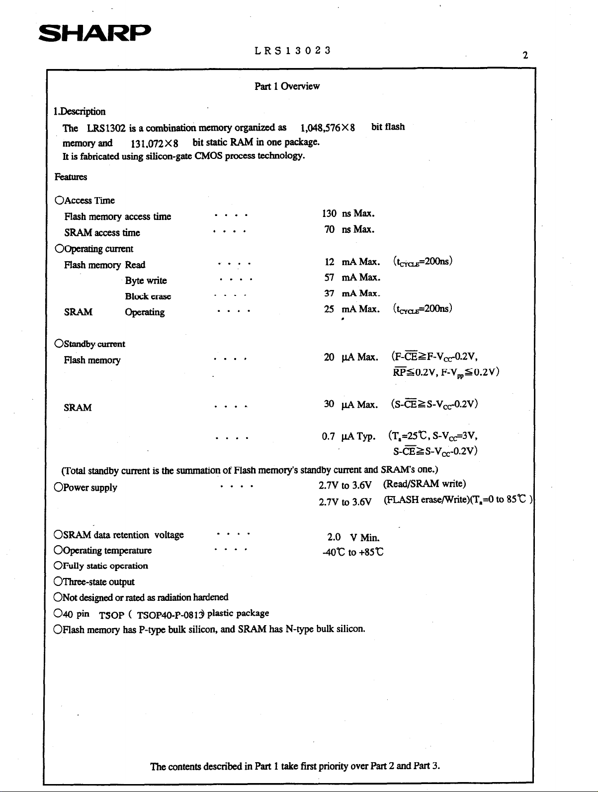
l.Description
The LRS1302 is a combination memory organized as
memory and
It is fabricated using silicon-gate CMOS process technology.
Features
OAccess Time
Flashmemoryaccesstime
SRAM access time
OOpemtingcurrent
Flash memory Read
SRAM
131,072X8
Byte write
Block erase
operatin%
bit static RAM in one package.
- * * *
. . . .
. . . .
. . . .
. . . .
- - * *
1448,576 X 8
130 nsMax.
70 nsMax.
12 mAMax. (t&ti2OOns)
57 r&Max.
37 mAMax.
25 mA Max. hcxJz.=2=)
,
bit flash
2
ostandbycurrent
Flash memory
Sk4M
(Total standby curnat is the summation of Flash memory’s standby current and SRAM’s one.)
OPower supply
OSRAM data retention voltage
OOperating temperature
OFully static operation
oThree-state output
ONot designed or rated as radiation hardened
040 pin TSOP ( TSOP~O-p-0819 plastic package
OFlash memory has P-type bulk silicon, and SRAh4 has N-type bulk silicon.
. . . .
. . . .
. . . .
. . . .
. . . .
20 @ Max. (F-EZF-Vc,0.2V,
EbO.2V, F-V&O.2V)
30 pA Max. (S-EZS-Vc,0.2V)
0.7 @ Typ. (T,=25”c, S-V,-3V,
S-CErs-Vcc-0.2V)
2.7V to 3.6V @ead/SRAM write)
2.7~ to 3.6~ @LASH erase/write)(T,=O to 85c
2.0 V Min.
40°C to +85”c
The contents described in Part 1 take first priority over Part 2 and Part 3.
Page 4
-
SHARP
LRS13023
Part 1 Overview
l.Description
The LRS1302 is a combination memory organized as
memory and
It is fabricated using silicon-gate CMOS process technology.
OAccess Time
Flashmemoryaccesstime
SRAM access time
OOpemtingcment
Flash memory Read
SRAM Operating
131,072X8
Byte write
Block erase
bit static RAM in one package.
- * * *
. . . .
. . . .
. . . .
. . . .
- - * *
1,048,576X 8 bit flash
130 nsMax.
70 nsMax.
12 mAMax. (t&ti2Oons>
57 mAMax.
37 mAMax.
25 mAMax.
,
hcxJ&oons)
2
ostandbycurrent
Flash memory
Sk4M
(Total standby current is the summation of Flash memory’s standby current and SRAM’s one.)
3Power supply
3SRAM data retention voltage
3Operating temperature
IFully static operation
3Three-state output
JNot designed or rated as radiation hardened
240 Pin TSOP ( TSOP~O-p-0819 plastic package
IFlash memory has P-type bulk silicon, and SRAM has N-type bulk silicon.
. . . .
. . . .
. . . .
. . . .
. . . .
20 pA Max. (F-EZF-Vc,0.2V,
EbO.2V, F-V&O.2V)
30 @ Max. (S-=ZS-Vc,0.2V)
0.7 @ Typ. (T,=25”c, S-V,-3V,
s-CEZS-vcc-0.2v)
2.7V to 3.6V @ead/SPAM write)
2.7~ to 3.6~ (FLASH erase/write>Cr,=O to 85c
2.0 V Min.
40°C to +85”c
The contents described in Part 1 take first priority over Part 2 and Part 3.
Page 5
m
.
Page 6
SHARI=
LRS13023
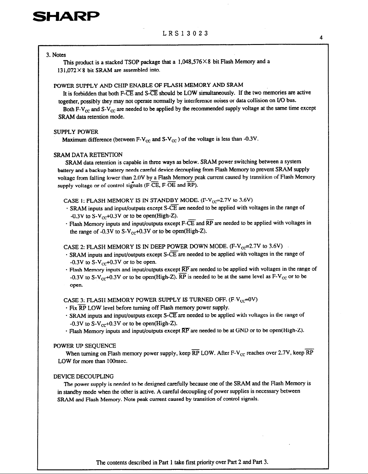
3. Notes
This product is a stacked TSOP package that a 1,048,576X 8 bit Flash Memory and a
13 1,072 X 8 bit SRAM are assembled into.
POWER SUPPLY AND CHIP ENABLE OF FLASH MEMORY AND SRAM
It is forbidden that both F-E and S-E should be LOW simultaneously. If the two memories are active
together, possibly they may not operate normally by interference noises or data collision on I/O bus.
Both F-V, and S-V, are needed to be applied by the recommended supply voltage at the same time except
SRAM data retention mode.
SUPPLY POWER
Maximum difference (between F-V,
SRAM DATA RETENTION
SRAM data retention is capable in three ways as below. SRAM power switching between a system
battery and a backup battery needs careful
voltage from
supply voltage or of control si{nals (F-B, F-?% and RP).
CASE I: FLASH MEMORY IS IN STANDBY MODE. (F-Vcc=2.7V to 3.6V)
* SRAM inputs and input/outputs except S-mare needed to be applied with voltages in the range of
-0.3V to S-Vcc+O.3V or to be open(High-Z).
* Flash Memory inputs and input/outputs except F-eand Gare needed to be applied with voltages in
the range of -0.3V to S-V,,+O.3V or to be open(High-Z).
failing
lower han
2.OV by a Flash Memory peak current caused by transition of Flash Memory
and S-V, ) of the voltage is less than -0.3V.
device
decoupling from Flash Memory to prevent SRAM
4
supply
CASE 2: FLASH MEMORY IS IN DEEP POWER DOWN MODE. (F-Vcc=2.7V to 3.6V)
* SRAM inputs and input/outputs except S-mare needed to be applied wilh voltages in the range of
-0.3V to S-V,c+O.3V or to be open.
* Flash Memory inputs and input/outputs except mare needed to be applied with voltages in the range of
-0.3V to S-Vc,+O.3V or to be open(High-Z). RP is needed to be at the same level as F-V,, or to be
open.
CASE 3: FLASH MEMORY POWER SUPPLY IS TURNED OFF. (F-VcpOV)
* Fix- LOW level before turning off Flash memory power supply.
* SRAM inputs and input/outputs except S-mare needed to be applied with voltages in the range of
-0.3V to S-V,c+O.3V or to be open(High-Z).
- Flash Memory inputs and input/outputs except mare needed to be at GND or to be open(High-Z).
POWER UP SEQUENCE
When turning on Flash memory power supply, keep i@ LOW. After F-V,, reaches over 2.7V, keep RP
LOW for more than 1OOnsec.
DEVICE DECOUPLING
The power supply is needed to be designed carefully because one of the SRAM and the Flash Memory is
in standby mode when the other is active. A careful decoupling of power supplies is necessary between
SRAM and Flash Memory. Note peak current caused by transition of control signals.
The contents described in Part 1 take first priority over Part 2 and Part 3.
Page 7
SHARP
LRS13023
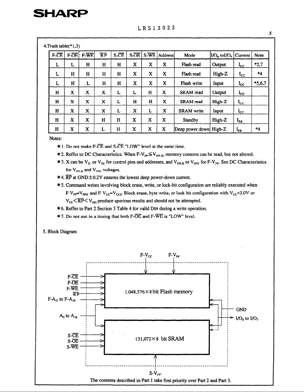
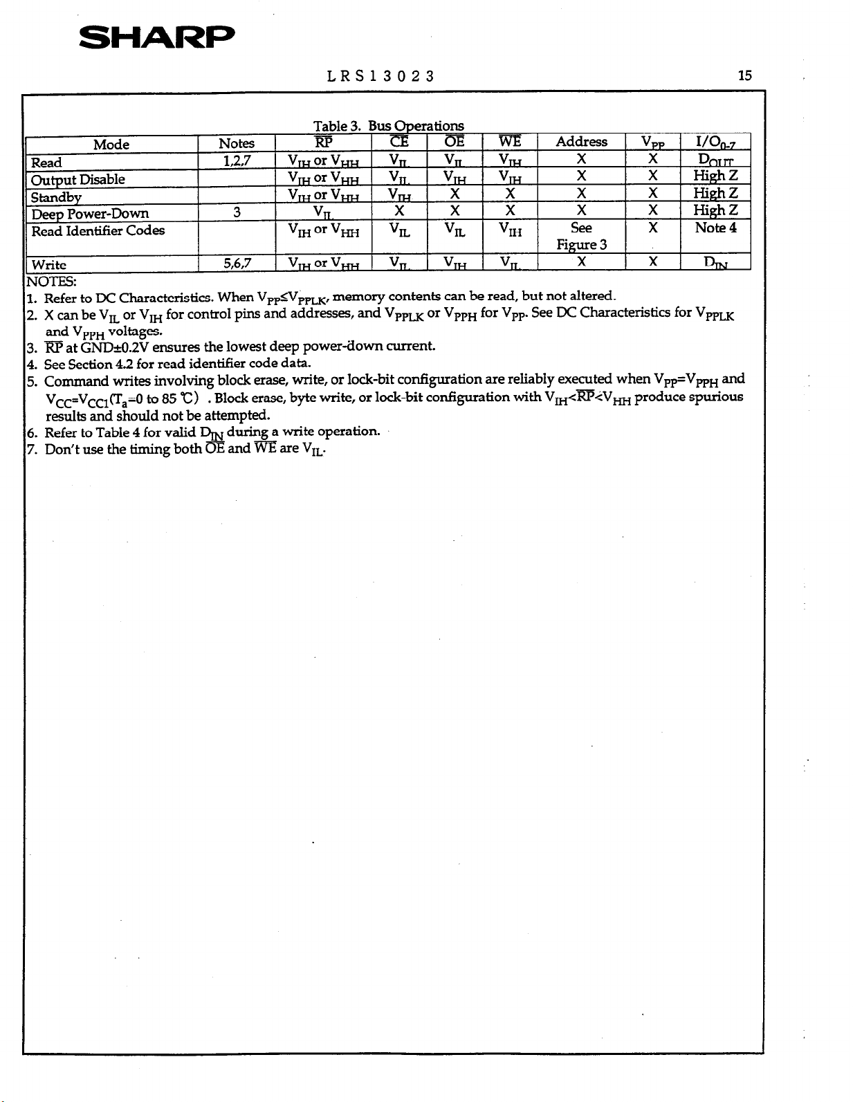
4.Truth table(* 1.3)
F-a F-m F-m RP S-a S-m S-m Address Mode I/O, toI/O, Current Note
LLHHHXXX Flash read output
LHHHHXXX Flash read High-Z I,, *4
LHLHHXXX Flash write Input
HXXXLLHX SRAM read output Ice
HXXXLHHX sR4M read High-Z I,,
HXXXLXLX SRAM write Input I
HXXHHXXX Standby High-Z Iss
HXXLHXXX Deep power down High-Z Isa *4
Notes:
* 1. Do not make F-C? and S-C8 “LOW” level at the samc,limc.
* 2. Reffcr to DC Character&tics. When F-V&V,,.,.,, memory contents can be read, but not altered.
* 3. X can be V,,, or V,,, for control pins and addresses, and V,,nx or VI,,,,, for F-V,,,,. See DC Characteristics
for V,,,k and V,,.,, voltages.
* 4. i@ at GND f0.2V ensures the lowest deep power-down current.
* 5. Command writes involving block erase, write, or lock-bit configuration are reliably executed when
F-V,,=V,, and F-V,@,. Block erase, byte write, or lock-bit conliguration with Vcc<3.0V or
V,,, <m< V,,,, produce spurious results and should not be attempted.
* 6. Reffer to Part 2 Section 3 Table 4 for valid DIN during a write operation.
$7. Do not
use in
a timing that both F-mand F-WE is “LOW” level.
EC
kc
cc
5
*2,7
*5,6,7
5. Block Diagram
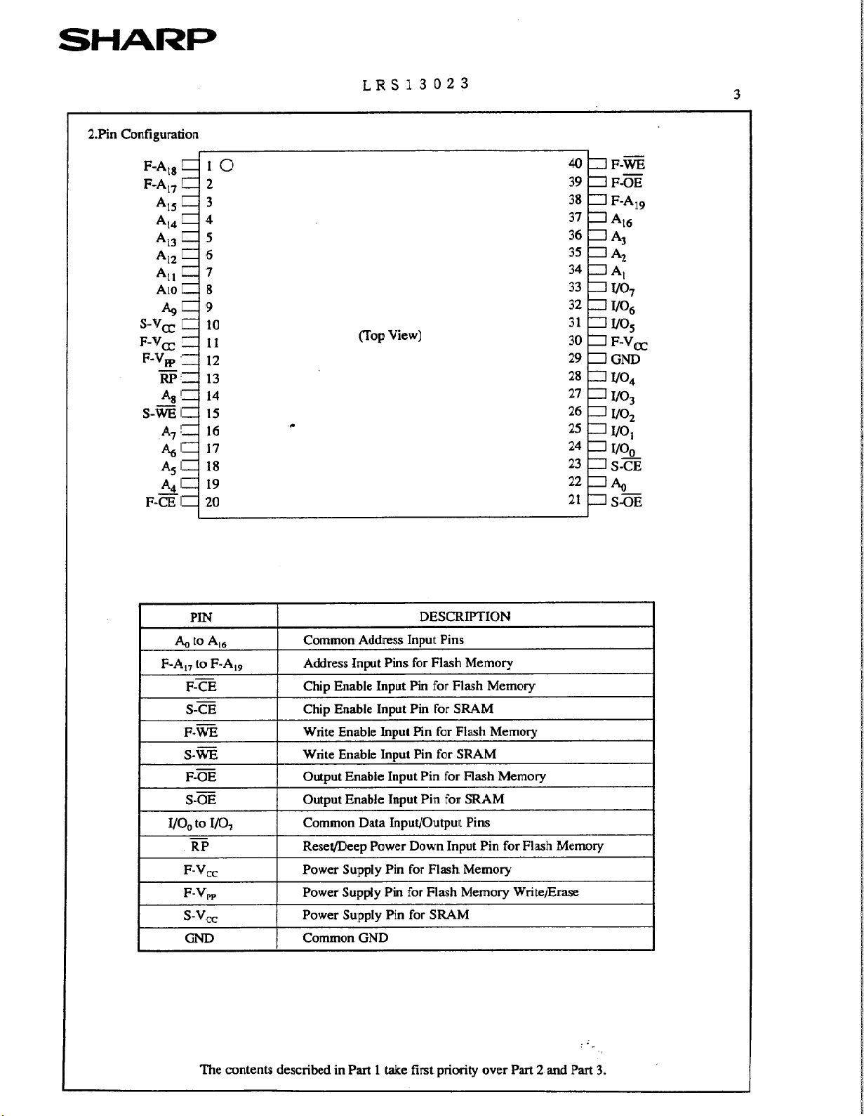
F-n i
F-GE / >
F-m j
RP ;
F-A,, to F-A,, !
&to&, ;
S-TE /
S-FE
s-m ;
F-V, F-V,,
____________________----------.------------------------------------------
9
w v
3
>
>
>
4
I
>
>
>
1,048,576 X 8
131,072X8
bit Flash memory
bit SR4M
I
e- ;
e
0
>
The contents described in Part 1 take first priority over Part 2 and Part 3.
Page 8
SHARP
LRS13023
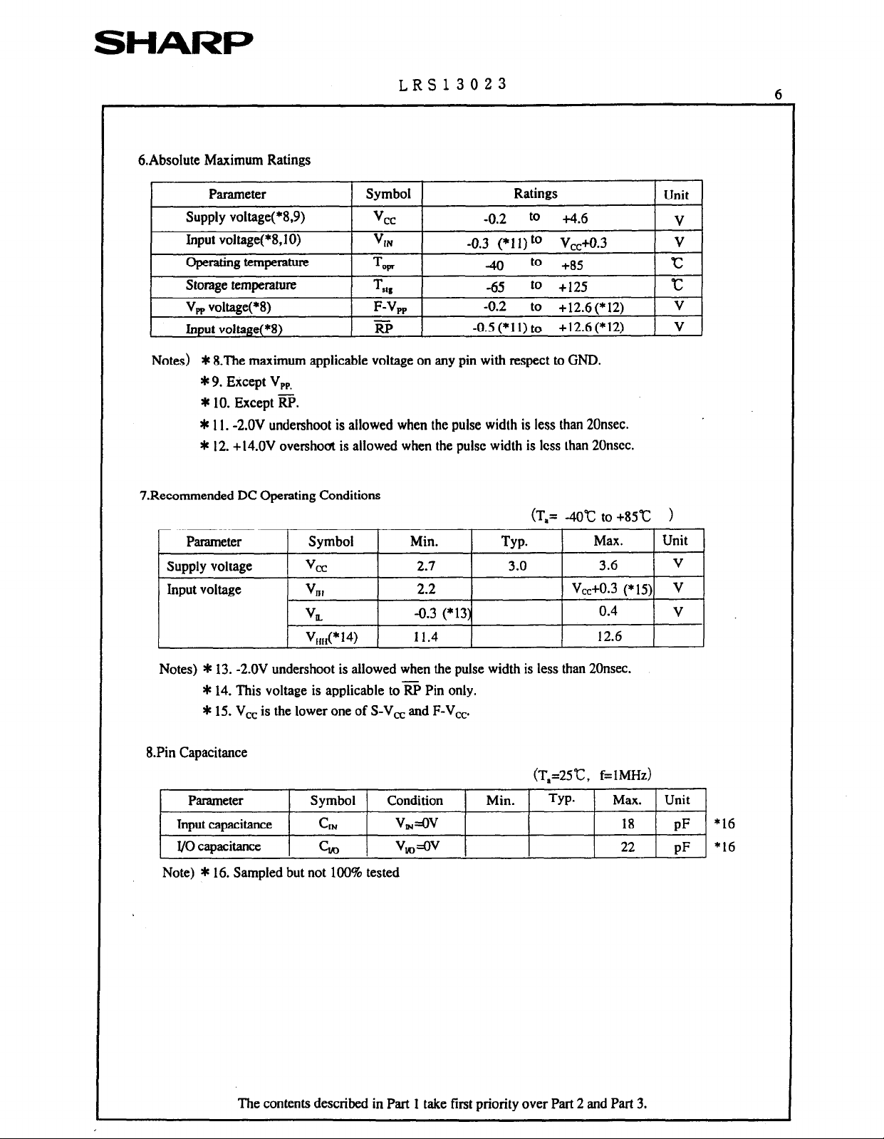
6.Absolute Maximum Ratings
Notes) * 8.The maximum applicable voltage on any pin with respect to GND.
* 9. Except Vrp,
* 10. Except @.
* 11. -2.OV undershoot is allowed when the pulse width is less than 20nsec.
* 12. +14.OV overshoot is allowed when the pulse width is less than 2Onscc.
7.Recommended DC Operating Conditions
CT,= -40°C to +85”c )
Parameter Symbol Min.
Supply voltage
Input voltage
vc-2
V”,
VU.
v,,,,(* 14)
2.7 3.0 3.6
2.2 V,,+O.3 (*15) V
-0.3 (*13:
11.4 12.6
TYP.
Max. Unit
V
0.4
V
6
Notes) * 13. -2.OV undershoot is allowed when the pulse width is less than 2Onsec.
* 14. This voltage is applicable toi@ Pin only.
* 15. V, is the lower one of S-V, and F-V,,.
8.Pin Capacitance
(T,=25”c, f=lMHz)
Parameter Symbol Condition
Input capacitance
I/O capacitance
Note) * 16. Sampled but not 100% tested
Gi
CIA3
v,=ov
v,=ov
Min. TYP.
Max. Unit
18
22
PF
PF
*16
*16
The contents described in Part 1 take first priority over Part 2 and Part 3.
Page 9
SHARP
LRS13023
Part2 Flash memory
CONTENTS
8
PAGE
.. INTRODUCTION
1.1 New Features.. ...........................................................
1.2 Product Overview
!. PRINCIPLES OF OPERATION
2.1 Data Protection
I.BUS OPERATION.. ........................................... .
3.1 Read
3.2 Output Disable
3.3 Standby
3.4 Deep Power-Down
3.5 Read Identifier Codes Operation
3.6 Write ...........................................................................
I. COMMAND DEFINITIONS
4.1 Read Array Command
4.2 Read Identifier Codes Command .........................
4.3 Read Status Register Command..
4.4 Clear Status Register
4.5 Block Erase Command
4.6 Byte Write Command ..............................................
4.7 Block Erase Suspend Command
4.8 Byte Write Suspend Command.. ...........................
4.9 Set Block and Master Lock-Bit Commands
........................................................................... 13
...................................................................... 13
........................................................... 9
......................................................
...................................
.........................................................
............
........................................
...................................................
.......................................
............................................ 17
Command
............................................ 17
;............... 13
........................... 14
..........................
...........................
...........................
.........
-9
9
12
12
13
13
14
14
.17
.17
.17
18
.18
.19
-19
PAGE
4.10 Clear Block Lock-Bits
5. DESIGN CONSIDERATIONS .................................... 28
5.1 Three-Line Output Control .................................... 28
5.2 Power Supply
5.3 V,, Trace on Printed Circuit Boards.. ................... 28
5.4 V,,, V,,, i?is Transitions.. ......................................
5.5 Power-Up/Down Protection.. ................................ 29
5.6 Power Dissipation.. .................................................. 29
6.ELECTRICAL SPECIFICATIONS ............................... 30
6 1 Absolute Maximum
6.2 Operating Conditions..
6.2.1 AC Input/Output Test Conditions.. ................ 31
6.2.2 DC Characteristics .............................................
6.2.3 AC Characteristics - Read-Only Operations
6.2.4 AC Characteristics - Write Operations..
6.2.5 Alternative a-Controlled Writes ................... 38
6.2.6 Reset Operations ................................................ 40
6.2.7 Block Erase, Byte Write and Lock-Bit
Configuration Performance.. ...........................
Decoupling.. .................................... 28
Command.. ....................... 20
29
Ratings.. ................................. 30
............................................ 30
32
... 34
.36
.........
41
Page 10
SHARP
LRS13023
Part2 Flash memory
CONTENTS
8
PAGE
.. INTRODUCTION
1.1 New Features.. ...........................................................
1.2 Product Overview
!. PRINCIPLES OF OPERATION
2.1 Data Protection
I.BUS OPERATION.. ........................................... . ............ 13
3.1 Read
3.2 Output Disable
3.3 Standby
3.4 Deep Power-Down
3.5 Read Identifier Codes Operation
3.6 Write ...........................................................................
I. COMMAND DEFINITIONS
4.1 Read Array Command
4.2 Read Identifier
4.3 Read Status Register Command..
4.4 Clear Status Register Command
4.5 Block Erase Command
4.6 Byte Write Command
4.7 Block Erase Suspend
4.8 Byte Write Suspend
4.9 Set Block and Master Lock-Bit Commands
........................................................................... 13
...................................................................... 13
...........................................................
......................................................
...................................
.........................................................
........................................
...................................................
....................................... 14
............................................ 17
Codes Command
............................................ 17
.............................................. 18
Command
Command..
;............... 13
........................... 14
.........................
..........................
...........................
...........................
...........................
.........
9
-9
9
12
12
13
14
.17
.17
.17
.18
.19
-19
PAGE
4.10 Clear Block Lock-Bits Command.. ....................... 20
.........
28
.36
5. DESIGN CONSIDERATIONS ....................................
5.1 Three-Line Output Control .................................... 28
5.2 Power Supply
5.3 V,, Trace on Printed
5.4 V,,, V,,, i?is Transitions.. ...................................... 29
5.5 Power-Up/Down
5.6 Power Dissipation..
6.ELECTRICAL SPECIFICATIONS ............................... 30
6 1 Absolute Maximum
6.2 Operating Conditions..
6.2.1 AC Input/Output
6.2.2 DC Characteristics ............................................. 32
6.2.3 AC Characteristics - Read-Only Operations ... 34
6.2.4 AC Characteristics - Write Operations..
6.2.5 Alternative a-Controlled Writes ................... 38
6.2.6 Reset Operations ................................................ 40
6.2.7 Block Erase, Byte Write and Lock-Bit
Configuration Performance.. ........................... 41
Decoupling.. .................................... 28
Circuit Boards.. ................... 28
Protection.. ................................ 29
.................................................. 29
Ratings.. ................................. 30
............................................ 30
Test Conditions.. ................ 31
Page 11

SHARP
LRS13023
INTRODUCTION
his datasheet contains LRS1302 specifications.
iection 1 provides a flash memory overview. Sections
!, 3,4, and 5 describe the memory organization and
unctiordity. Section 6 covers electrical specifications.
..l New Features
The LRS1302 SmartVoltage Flash memory maintains
)ackwards-compatibility with SHARP’s 28F008SA.
Cey enhancements over the 28F008SA include:
SmartVoltage Technology
*Enhanced Suspend Capabilities
Jn-System Block Locking
30th devices share a compatible, status register, and
oftware command set. These similarities enable a
clean upgrade from the 28FOO8SA to LRS1302. When
upgrading, it is important to note the following
iifferences:
-Because of new feature support, the two devices
have different device codes. This allows for
software optimization.
.VPpLK has been lowered from 6SV to 1.5V to
support 2.7V-3.6V block erase, byte write, and
lock-bit configuration operations. Designs
switch VPP off during read operations should make
sure that the VP, voltage transitions to GND.
*To take advantage of SmartVoltage technology,
allow VP, connection to 2.7V-3.6V.
that
SmartVoltage technology provides a choice of Vcc and
VP, combinations, as shown in Table 1, to meet system
performance and power expectations. V, at 2.7V to
3.6V eliminates the need for a separate 12V converter.
In addition to flexible erase and program voltages, the
dedicated VPP pm gives complete data protection
when VP, I VP,,.
Table 1. V,, and VP, Voltage Combinations Offered
;_.
2,7V to 3.6V(‘l) 2.7V to 3.6V
NOTE’ ’
‘1. FLASH Erase/Write(T*=O”C to 85°C)
Internal Vcc and
automatically configures the device for optimized read
and write operations.
A Command User Interface (CUT) serves as the
interface between the system processor and internal
operation of the device. A valid command sequence
written to the CUT initiates device automation. An
internal Write State Machine (WSM) automatically
executes the algorithms and timings necessary for
block erase, byte write, and lock-bit configuration
operations.
A block erase operation erases one of the device’s
64Kbyte blocks typically within 1.8 second
independent of other blocks. Each block can be
independently erased 100,000 times (1.6 million block
erases per device). Block erase suspend mode allows
system software to suspend block erase to read or
write data from any other block.
by SmartVoltage Technology
Vcc Voltage VPP Voltage
VW
detection Circuitry
9
I
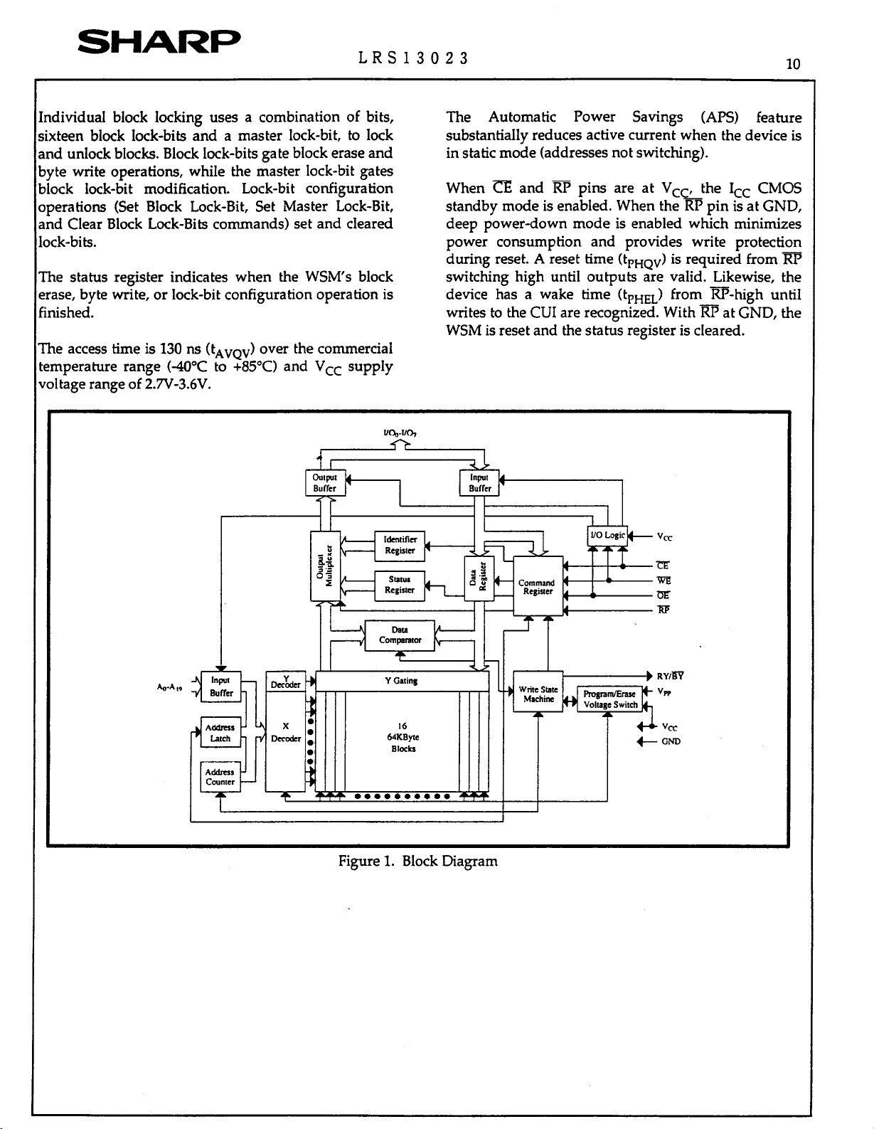
I.2 Product Overview
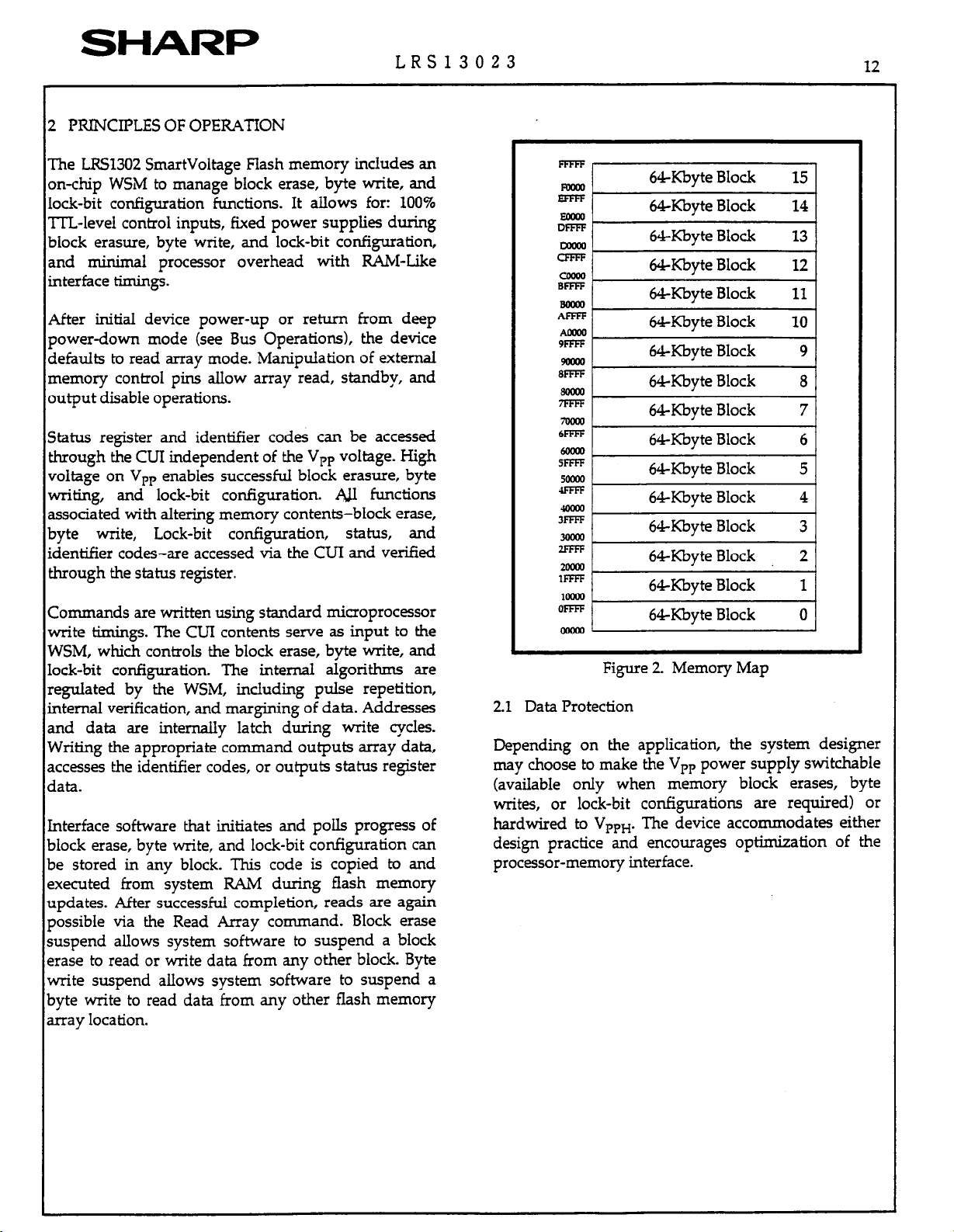
The LRS1302 is a high-performance &Mbit
;martVoltage Flash memory organized as 1 Mbyte of 8
>its. The 1 Mbyte of data is arranged in sixteen
&Kbyte blocks which are individually erasable,
o&able, and unlockable in-system. The memory map
s shown in Figure 2.
Writing memory data is performed in byte increments
typically within 17 us. Byte write suspend mode
enables the system to read data or execute code from
any other flash memory array location.
1
Page 12
SHARP
LRS13023
10
~Individual block locking uses a combination of bits,
‘sixteen block lock-bits and a master lock-bit, to lock
land unlock blocks. Block lock-bits gate block erase and
‘byte write operations, while the master lock-bit gates
~block lock-bit modification. Lock-bit configuration
loperations (Set Block Lock-Bit, Set Master Lock-Bit,
and Clear Block Lock-Bits commands) set and cleared
lock-bits.
The status register indicates when the WSM’s block
erase, byte write, or lock-bit configuration operation is
finished.
The access time is 130 ns (tAvQv) over the commercial
temperature range (-40°C to +BS’C) and V,, supply
voltage range of 2.7V-3.6V.
The Automatic Power Savings (AI%) feature
substantially reduces active current when the device is
in static mode (addresses not switching).
When a and RF pins are at V,,, the I,, CMOS
standby mode is enabled. When the RP pin is at GND,
deep power-down mode is enabled which minimizes
power consumption and provides write protection
during reset. A reset time (tPHqv) is required from RP
switching high until outputs are valid. Likewise, the
device has a wake time (tpHEL) from m-high until
writes to the CUI are recognized. With RP at GND, the
WSM is reset and the status register is cleared.
4 x :
occcdc.r .
16
64KByle
.
BlOCb
Figure 1. Block Diagram
Page 13
SHARP
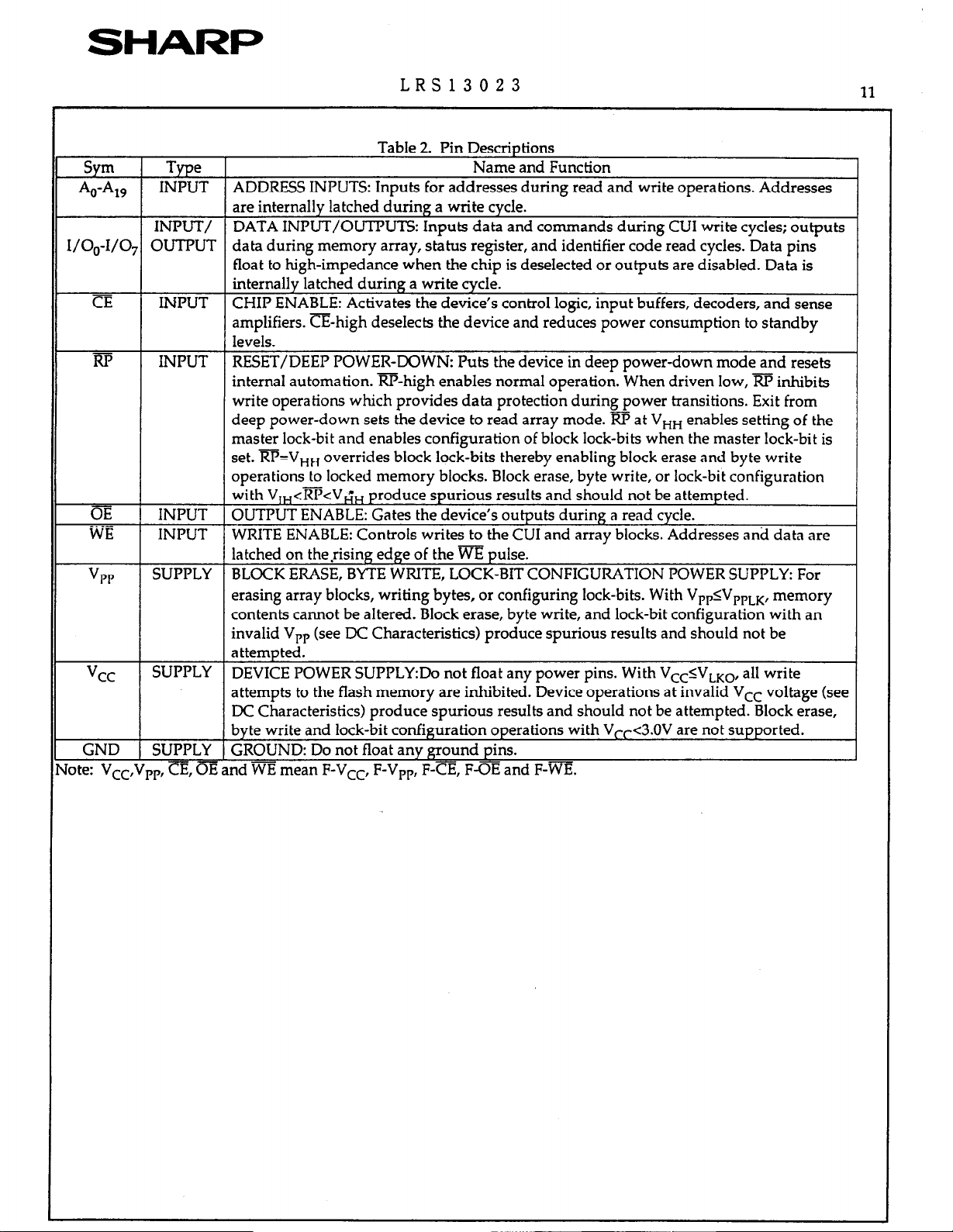
Svm
f40-419
I/O&O~
CE
Rp
OE
_. _-
WE
bP
Vcc
GND
rote: V,-,
LRS13023
Table 2. Pin Descriptions
Type
INPUT
INPUT/
OUTPUT
INPUT
INPUT
INPUT
INPUT
SUPPLY
SUPPLY
SUPPLY GROUND: Do not float any ground pins.
,P, n, m and WE mean F-V,,, F-V,,, F-a, Fa and F-WE.
ADDRESS INPUTS: Inputs for addresses during read and write operations. Addresses
are internally latched during a write cycle.
DATA INPUT/OUTPUTS: Inputs data and commands during CUI write cycles; outputs
data during memory array, status register, and identifier code read cycles. Data pins
float to high-impedance when the chip is deselected or outputs are disabled. Data is
internally latched during a write cycle.
CHIP ENABLE: Activates the device’s control logic, input buffers, decoders, and sense
amplifiers. a-high deselects the device and reduces power consumption to standby
levels.
RESET/DEEP POWER-DOWN: Puts the device in deep power-down mode and resets
internal automation. m-high enables normal operation. When driven low, p inhibits
write operations which provides data protection during power transitions. Exit from
deep power-down sets the device to read array mode. Ris at V,, enables setting of the
master lock-bit and enables configuration of block lock-bits when the master lock-bit is
-
set. RP=V,,, overrides block lock-bits thereby enabling block erase and byte write
operations to locked memory blocks. Block erase, byte write, or lock-bit configuration
with V,,<RI’cV& produce spurious results and should not be attempted.
OUTPUT ENABLE: Gates the device’s outputs during a read cycle.
WRITE ENABLE: Controls writes to the CUI and array blocks. Addresses
latched
BLOCK ERASE, BYTE WRITE, LOCK-BIT CONFIGURATION POWER SUPPLY: For
erasing array blocks, writing bytes, or configuring lock-bits. With VPP5VPPLK, memory
contents cannot
invalid VP, (see DC Characteristics) produce spurious results and should not be
attempted.
DEVICE POWER SUPPLYDo not float any power pins. With VCCIVLKO, all write
attempts to the flash memory are inhibited. Device operations at invalid Vcc voltage (see
DC Characteristics) produce spurious results and should not be attempted. Block erase,
byte write and lock-bit configuration operations with V,,<3.OV are not supported.
on
the rising edge of the WE pulse.
be altered. Block erase, byte write, and lock-bit configuration with an
Name and Function
and
11
data are
Page 14
SHARI=
2 PRINCIPLES OF OPERATION
LRS13023
12
The LRS1302 SmartVoltage Flash memory includes an
on-chip WSM to manage block erase, byte write, and
lock-bit configuration functions. It allows for: 100%
TTL-level control inputs, fixed power supplies during
block erasure, byte write, and lock-bit configuration,
and minimal processor overhead with RAM-Like
interface timings.
After initial device power-up or return from deep
power-down mode (see Bus Operations), the device
defaults to read array mode. Manipulation of external
memory control pins allow array read, standby, and
output disable operations.
Status register and identifier codes can be accessed
through the CUI independent of the VP, voltage. High
voltage on V,, enables successful block erasure, byte
writing, and lock-bit configuration. All functions
associated with altering memory contents-block erase,
byte write, Lock-bit configuration, status, and
identifier codes-are accessed via the CUI and verified
through the status register.
Commands are written using standard microprocessor
write timings. The CUI contents serve as input to the
WSM, which controls the block erase, byte write, and
lock-bit configuration. The internal algorithms are
regulated by the WSM, including pulse repetition,
internal verification, and margining of data. Addresses
and data are internally latch during write cycles.
Writing the appropriate command outputs array data,
accesses the identifier codes, or outputs status register
data.
Interface software that initiates and polls progress of
block erase, byte write, and lock-bit configuration can
be stored in any block. This code is copied to and
executed from system RAM during flash memory
updates. After successful completion, reads are again
possible via the Read Array command. Block erase
suspend allows system software to suspend a block
erase to read or write data from any other block. Byte
write suspend allows system software to suspend a
byte write to read data from any other flash memory
array location.
I
I
Aoooo
9FFFF
9oMw)
SFFFF
8oooO
7FFFF
7owo
6FFFF
t5wlo
SFFFF
2Izzz
I
I
mm
OFFFF
ooom
2.1 Data Protection
Depending on the application, the system designer
may choose to make the V,, power supply switchable
(available only when memory block erases, byte
writes, or lock-bit configurations are required) or
hardwired to V,,,.
design practice and encourages optimization of the
processor-memory interface.
64Kbyte Block
64-Kbyte Block
64Kbyte Block 4 1
64Kbyte Block
64Kbyte Block 0
Figure 2. Memory Map
The device accommodates either
15 I
10 I
l/
Page 15
SHARI=
LRS13023
When VPPIVPPLK, memory contents cannot be altered.
The CUI, with two-step block erase, byte write, or
lock-bit configuration command sequences, provides
protection from unwanted operations even when high
voltage is applied to VP+. All write functions are
disabled when V,,
VLKO or when RP is at Vl,. The device’s block locking
capability provides additional protection from
inadvertent code or data alteration by gating erase and
byte write operations.
3 BUS OPERATION
The local CPU reads and writes flash memory
in-system. All bus cycles to or from the flash memory
:onform to standard microprocessor bus cycles.
3.1 Read
Information can be read from any block, identifier
:odes, or status register independent of the VP,
voltage. RP can be at either Vl, or V,,.
The first task is to write the appropriate read mode
:ommand (Read Array, Read Identifier Codes, or Read
status Register) to the CUI. Upon initial device
Tower-up or after exit from deep power-down mode,
:he device automatically resets to read array mode.
Four control pins dictate the data flow in and out of
:he component: CE, OE, WE, and m. CE and m must
>e driven active to obtain data at the outputs. m is the
device selection control, and when active enables the
ielected memory device. m is the data output
I/O&O,) control and when active drives the
ielected memory data onto the I/O bus. WE must be
it VI, and m must be at V,, or V,,. Figure 12
llustrates a read cycle.
1.2 Output Disable
Mith 0lY at a logic-high level (Vt,), the device outputs
Ire disabled. Output pins I/0,-1/0, are placed in a
high-impedance state.
is below the write lockout voltage
.c
---
13
3.3 Standby
n at a logic-high level (V,,) places the device in
standby mode which substantially reduces device
power consumption. I/O&O, outputs are placed in
a high-impedance state independent of OE. If
deselected during block erase, byte write, or lock-bit
configuration, the device continues functioning, and
consuming active power until the operation completes.
3.4 Deep Power-Down
i?Ij at V,, initiates the deep power-down mode.
In read modes, m-low deselects the memory, places
output drivers in a high-impedance state and turns off
all internal circuits. RP must be held low for a
minimum of 100 ns. Time tPHQv is required after
return from power-down until initial memory access
outputs are valid. After this wake-up interval, normal
operation is restored. The CUI is reset to read array
mode and status register is set to 80H.
During block erase, byte write, or lock-bit
configuration modes, m-low will abort the operation.
Memory contents being altered are no longer valid; the
data may be partially erased or written. Time tpHWL is
required after Rp goes to logic-high (VI,) before
another command can be written.
As with any automated device, it is important to assert
Rp during system reset. When the system comes out of
reset, it expects to read from the flash memory.
Automated flash memories provide status information
when accessed during block erase, byte write, or
lock-bit configuration modes. If a CPU reset occurs
with no flash memory reset, proper CPU initialization
may not occur because the flash memory may be
providing status information instead of array data.
SHARP’s flash memories allow proper CPU
initialization following a system reset through the use
of the i?l? input. In this application, Rp is controlled by
the same m signal that resets the system CPU.
Page 16
SHARP
LRS13023
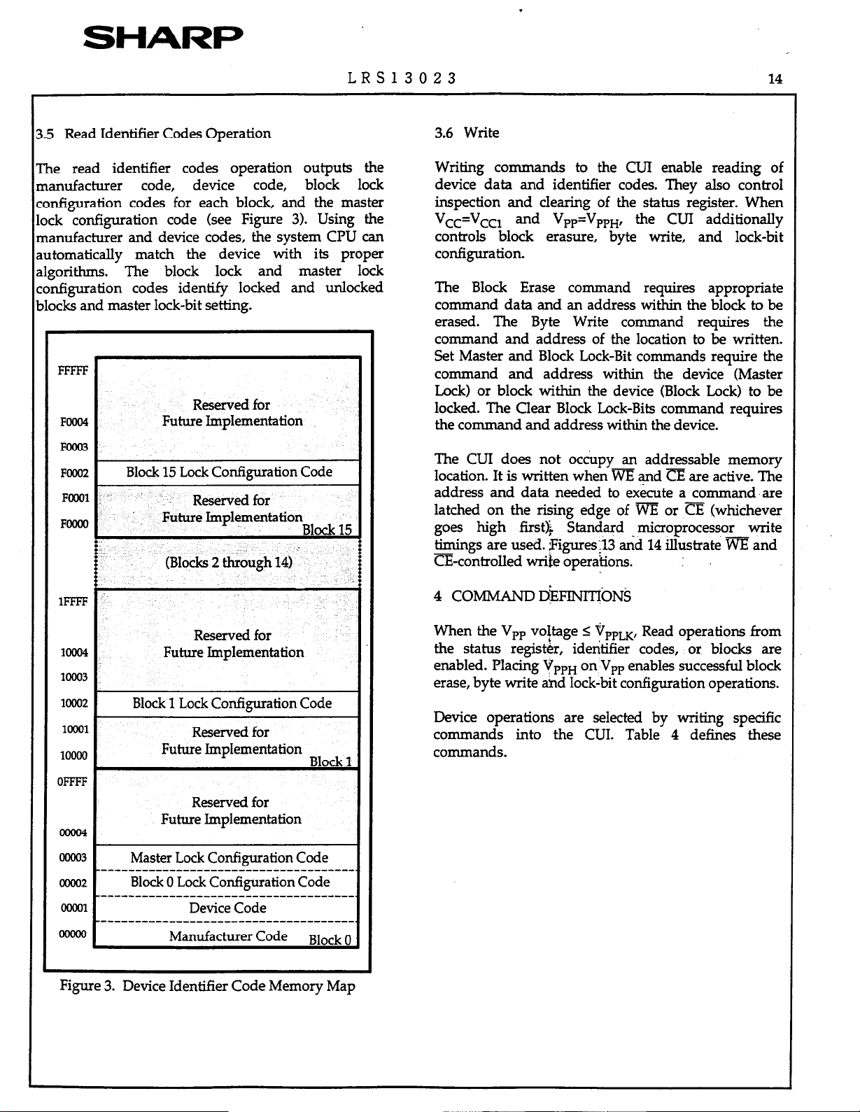
1.5 Read Identifier Codes Operation
The read identifier codes operation outputs the
nanufacturer code, device code, block lock
:onfiguration codes for each block, and the master
ock configuration code (see Figure 3). Using the
nanufacturer and device codes, the system CPU can
u,rtomatically match the device with its proper
algorithms. The block lock and master lock
:onfiguration codes identify locked and unlocked
~1ock.s and master lock-bit setting.
Reserved for
FOO04
FOOO3
FOOOZ 1
FOOOl
FOOOO
Future Implementation
Block 15 Lock Configuration Code
Reserved for
Future Implementation
Block 1
(Blocks 2 through 14) ’
14
3.6 Write
Writing commands to the CUI enable reading of
device data and identifier codes. They also control
inspection and clearing of the status register. When
V,--=Vccl and VPP=VPPH, the CUI additionally
controls block erasure, byte write, and lock-bit
configuration.
The Block Erase command requires appropriate
command data and an address within the block to be
erased. The Byte Write command requires the
command and address of the location to be written.
Set Master and Block Lock-Bit commands require the
command and address within the device (Master
Lock) or block within the device (Block Lock) to be
locked. The Clear Block Lock-Bits co
mmand requires
the command and address within the device.
The CUI does not occupy an addressable memory
location. It is written when WE and a are active. The
address and data needed to execute a command-are
latched on the rising edge of WE or CE (whichever
goes high first& Stand,ard microprocessor write
timings are used. jQures:13 and 14 illustrate WE and
m-controlled write operahons.
:
IFFFF
Reserved for
looo4
1ooo3
I
Future Implementation
Block 1 Lock Configuration Code
OFFFF
Reserved for
Future Implementation
oooo4
oooo3
moo2
ooml
Master Lock Configuration Code
------------------------------------.
Block 0 Lock Configuration Code
~~~~~~~~----__-__---________________(
--------_-__________----------------.
Device Code
Manufacturer Code
Block
Figure 3. Device Identifier Code Memory Map
4 COMMAND D&INITlON~
When the VP, voftage I VPPLK, Read operations from
the status register, identifier codes, or blocks are
enabled. Placing VP,, on.Vpp enables successful block
erase, byte write and lock-bit configuration operations.
Device operations are selected by writing specific
commands into the CUI. Table 4 defines these
commands.
Page 17
SHARP
LRS13023 15
NOTES:
1. Refer to DC Characteristics. When VPPIVPP,,
2. X can be VI, or V,, for control pins and addresses, and VP,, or VP,, for VP,. See DC Characteristics for VW,
and V,,, voltages.
3. i@ at GND&.2V ensures the lowest deep power-down current.
4. See Section 4.2 for read identifier code data.
5. Command writes involving block erase, write, or lock-bit configuration are reliably executed when VPp=VppH and
Vcc=VccIU~=O to 85 “c)
results and should not be attempted.
6. Refer to Table 4 for valid h during a write operation.
7. Don’t use the timing both m and m are VIM
. Block erase, byte write, or lock-bit configuration with V,<mkV, produce spurious
memory contents can be read, but not altered.
Page 18
SHARI=
LRS13023
16
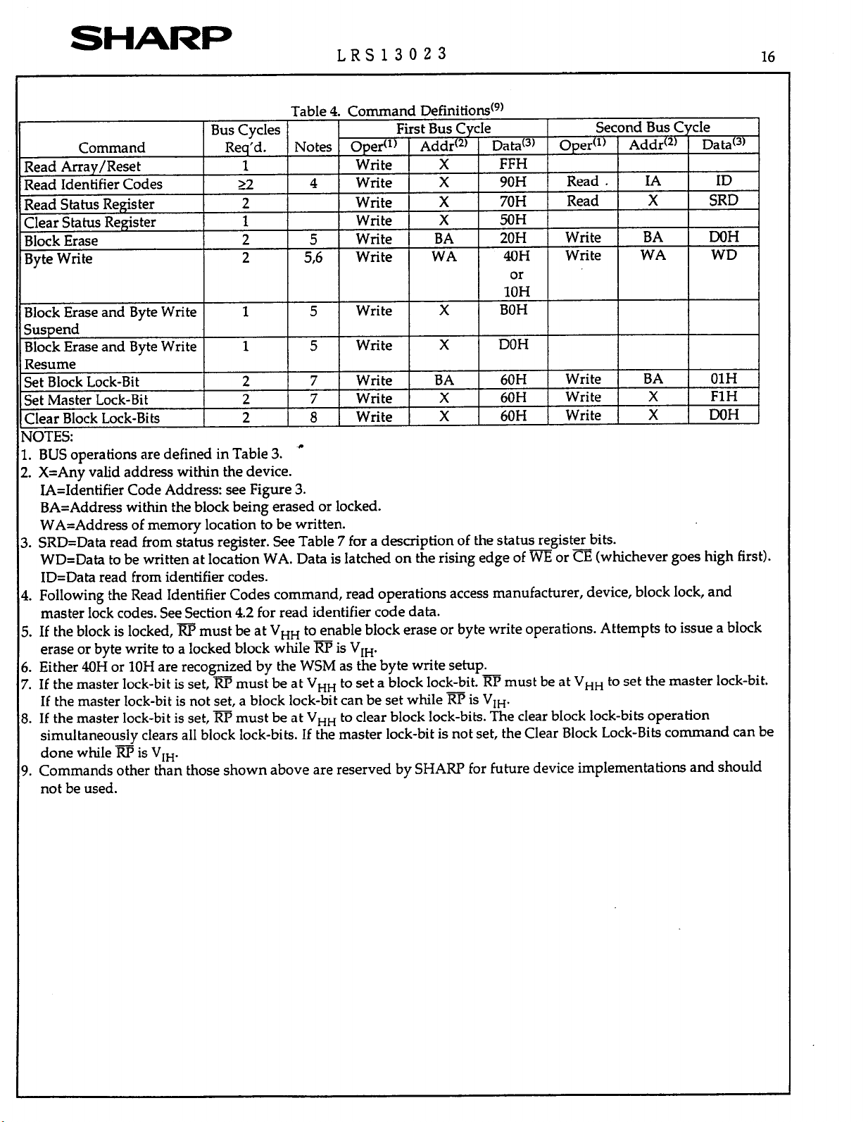
Table 4. Commanc - - ___._. ~_ _
RIW f-vr1c.c
Command
Read Array/Reset
Read Identifier Codes
Read Status Register
Clear Status Register 1
Block Erase 2 5
Byte Write
Req’d . Notes
1
22
2
2
56
Ope# ) Addrc2) 1 DataQ) Oper(l) 1 Addrt2) 1 Datac3)
Write X
4 Write X 90H
Write X 70H
Write X 5UH
Write BA 20H
Write WA 40H
I I I I
Block Erase and Byte Write
Suspend
Block Erase and Byte Write
Resume
Set Block Lock-Bit 2 7 Write BA 60H
Set Master Lock-Bit 2
Clear Block Lock-Bits 2 8 Write
NOTES:
1. BUS operations are defined in Table 3. ”
2. X=Any valid address within the device.
IA=Identifier Code Address: see Figure 3.
BA=Address within the block being erased or locked.
WA=Address of memory location to be written.
3. SRD=Data read from status register. See Table 7 for a description of the status register bits.
WD=Data to be written at location WA. Data is latched on the rising edge of WE or CE (whichever goes high first).
ID=Data read from identifier codes.
4. Following the Read Identifier Codes command, read operations access manufacturer, device, block lock, and
master lock codes. See Section 4.2 for read identifier code data.
5. If the block is locked, i?i? must be at V,,
erase or byte write to a locked block while m is VII+
6. Either 40H or 10H are recognized by the WSM as the byte write setup.
7. If the master lock-bit is set, m must be at V,,
If the master lock-bit is not set, a biock lock-bit can be set while i?is is V,,.
8. If the master lock-bit is set, RP must be at V,, to clear block lock-bits. The clear block lock-bits operation
simultaneously clears all block lock-bits. If the master lock-bit is not set, the Clear Block Lock-Bits command can be
done while RR 1s Vl,.
9. Commands other than those shown above are reserved by SHARP for future device implementa lions and should
not be used.
-.
1
1
5 Write
5 Write
7 Write X 60H
to enable block erase or byte write operations. Attempts to issue a block
to set a block lock-bit. RP must be at V,, to set the master lock-bit.
1 Definitions(9)
Fist Bus Cycle Second Bus Cycle
---- I
FFH
Read. IA ID
_. ----
or I
10H
X BOH
X
X 60H Write X DOH
DOH
Read X
Write BA
Write WA WD
I I
Write BA OlH
Write X FlH
I
SRD
DOH
I
Page 19
SHARP
.
LRS13023
:.l Read Array Command
Jpon initial device power-up and after exit from deep
jowerdown mode, the device defaults to read array
node. This operation is also initiated by writing the
lead Array command. The device remains enabled for
eads until another command is written. Once the
nternal WSM has started a block erase, byte write or
sck-bit configuration, the device will not recognize
he Read Array command until the WSM completes its
lperation unless the WSM is suspended via an Erase
luspend or Byte Write Suspend command. The Read
bray command functions independently of the VP,
poltage and m can be V,, or V,,.
,.2 Read Identifier Codes Command
‘he identifier code operation is initiated by writing the
Lead Identifier Codes command. Following the
ommand write, read cycles from addresses shown in
‘igure 3 retrieve the manufacturer, device, block lock
onfigura tion and master lock configuration codes (see
‘able 5 for identifier code values). To terminate the
Nperation, write another valid command. Like the
Lead Array command, the Read Identifier Codes
ommand functions independently of the VP, voltage
-
nd RP can be V,, or V,,. Following the Read
dentifier Codes command, the following information
an be read:
Table 5. Identifier Codes
17
4.3 Read Status Register Command
The status register may be read to determine when a
block erase, byte write, or, lock-bit configuration is
complete and whether the operation completed
successfully. It may be read at any time by writing the
Read Status Register command. After writing this
command, all subsequent read operations output data
from the status register until another valid command
is written. The status register contents are latched on
the falling edge of OE or CE, whichever occurs. OE or
iZ must toggle to V,,
the status register latch. The Read Status Register
command functions independently of the VP, voltage.
Rp can be V,, or V,,.
4.4 Clear Status Register Command
Status register bits SR.5, SR.4, SR.3, and SR.1 are set to
“1”s by the WSM and can only be reset by the Clear
Status Register command. These bits indicate various
failure conditions (see Table 7). By allowing system
software to reset these bits, several operations (such as
cumulatively erasing or locking multiple blocks or
writing several bytes in sequence) may be performed.
The status register may be polled to determine if an
error occurre during the sequence.
To clear the status register, the Clear Status Register
command (50H) is written. It functions independently
of the applied VP, Voltage. RP can be V,, or V,,.
This command is not functional during block erase or
byte write suspend modes.
before further reads to update
Block Lock Configuration
.Block is Unlocked
*Block is Locked
-Reserved for Future Use
Master Lock Configuration
SDevice is Unlocked
,Device is Locked
,Reserved for Future Use
IOTE:
. X selects the specific block lock configuration code
to be read. See Figure’3 for the device identifier
code memory map.
4.5 Block Erase Command
Erase is executed one block at a time and initiated by a
two-cycle command. A block erase setup is first
written, followed by an block erase confirm. This
command sequence requires appropriate sequencing
and an address within the block to be erased (erase
changes all block data to FFH). Block preconditioning,
erase, and verify are handled internally by the WSM
(invisible to the system). After the two-cycle block
erase sequence is written, the device automatically
outputs status register data when read (see Figure 4).
The CPU can detect block erase completion by
analyzing status register bit SR.7.
Page 20

SHARP
LRS13023
When the block erase is complete, status register bit
SR.5 should be checked. If a block erase error is
detected, the status register should be cleared before
system software attempts corrective actions. The CLJI
remains in read status register mode until a new
command is issued.
This two-step command sequence of set-up followed
by execution ensures that block contents are not
accidentally erased. An invalid Block Erase command
sequence will result in both status register bits SR.4
and SR.5 being set to “1”. Also, reliable block erasure
can only occur when Vcc=VccI and V,=V,,,. In the
absence of this high voltage, block contents are
protected against erasure. If block erase is attempted
while Vppflppm,
Successful block erase requires that the corresponding
block lock-bit be cleared or, if set, that m=V,. If
block erase is attempted when the corresponding
block lock-bit is set and m=V,,, SR.1 and SR5 wi.lI be
set to “1”. Block erase operations with V,<pcV,
produce spurious results and should not be attempted.
SR.3 and SR5 will be set to “1”.
18
register bits SR3 and SR4 will be set to “1”. Successful
byte write requires that the corresponding block
lock-bit be cleared or, if set, that i@=V,. If byte write
is attempted when the corresponding block lock-bit is
set and RP=V,,,
write operations with VI,<m<V,, produce spurious
results and should not be attempted.
4.7 Block Erase Suspend Command
The Block Erase Suspend command allows block-erase
interruption to read or byte-write data in another
block of memory. Once the block-erase process starts,
writing the Block Erase Suspend command requests
that the WSM suspend the block erase sequence at a
predetermined point in the algorithm. The device
outputs status register data when read after the Block
Erase Suspend command is written. Polling status
register bits SR.7 and SR.6 can determine when the
block erase operation has been suspended (both will
be set to “1”). Specification tw- defines the block
erase suspend latency. I I .%
SR.l and SR4 will be set to “1”. Byte
4.6 Byte Write Command
Byte
write is executed by a two-cycle command
sequence. Byte write setup (standard 40H or alternate
10H) is written, followed by a second write that
specifies the address and data (latched on the rising
edge of WE). The WSM then takes over, controlling the
byte
write and write verify algorithms internally. After
the byte write sequence is written, the device
automatically outputs status register data when read
[see Figure 5). The CPU can detect the completion of
the byte write event by analyzing status register bit
3R.7.
When byte write is complete, status register bit SR.4
should be checked. If byte write error is detected, the
status register should be cleared. The internal WSM
verify only detects errors for “1% that do not
juccessfully write to “0”s. The GUI remains in read
jtatus register mode until it receives another
:ommand.
&liable byte writes can only occur when V,c=VccI
md Vpp=Vppw
nemory contents are protected against byte writes. If
>yte write is attempted while VpplVppm, status
In the absence of this high voltage,
At this point, a Read Arraycomman
read data from blocks other than that which is
suspended. A Byte:Write comman
be issued during erase suspend to program data. in
other blocks. Using the Byte Write Suspend command
(see Section 4.81,. a..byte write operation can also. be
suspended. During-a byte write operation with block
erase suspended, status registerbit SR7 will return to
“0” . However, SR.6 will remain “1” to indicate block
erase suspend status.
The only other valid commands while block erase is
suspended are Read Status Register and Block Erase
Resume. After a Block Erase Resume command is
written to the flash memory, the WSM will continue
the block erase process. Status register bits SR.6 and
SR7 will automatically clear . After the Erase Resume
command is written, the device automatically outputs
status register data when read (see Figure 6). VP, must
remain at VP,, (the
erase) while block erase is suspended. m must also
remain at VI, or V, (the same m level used for
block erase). Block erase cannot resume until byte
write operations initiated during block erase suspend
have completed.
same
Vpp level used for block
d can be written to
d sequence can also
Page 21

SHARP
LRS13023
4.8 Byte Write Suspend Command
The Byte Write Suspend command allows byte write
interruption to read data in other flash memory
locations. Once the byte write process starts, writing
the Byte Write Suspend command requests that the
WSM suspend
predetermined point in the algorithm. The device
continues to output status register data when read
after the Byte Write Suspend command is written.
Polling status register bits SR.7 and SR.2 can determine
when the byte write operation has been suspended
(both will be set to “1”). Specification twHRHl defines
the byte write suspend latency.
At this point, a Read Array command can be written to
read data from locations other than that which is
suspended. The only other valid commands while byte
write is suspended are Read Status Register and Byte
Write Resume. After Byte Write Resume command is
written to the flash memory, the WSM will continue
the byte write process. Status register bits SR.2 and
SR7 will automatically clear. After the Byte Write
Resume command is written, the device automatically
outputs status register data when read (see Figure 7).
VP, must remain at V,, (the same VP, level used for
byte write) while in byte write suspend mode. m
must also remain at VrH or V, (the same Rp level
used for byte write).
4.9 Set Block and Master Lock-Bit Commands
A flexible block locking and unlocking scheme is
enabled via a combination of block lock-bits and a
master lock-bit. The block lock-bits gate program and
erase operations while the master lock-bit gates
block-lock bit modification. With the master lock-bit
not set, individual block lock-bits can be set using the
Set Block Lock-Bit command. The Set Master Lock-Bit
zommand, in conjunction with i@=V,, sets the
master lock-bit. After the master lock-bit is set,
subsequent setting of block lock-bits requires both the
Set Block Lock-Bit command and V, on the m pin.
see Table 6 for a summary of hardware and software
write protection options.
the byte write sequence at a
19
Set block lock-bit and master lock-bit are executed by a
two-cycle command sequence. The set block or master
lock-bit setup along with appropriate block or device
address is written followed by either the set block
lock-bit confirm (and an address within the block to be
locked) or the set master lock-bit confirm (and any
device address). The WSM then controls the set
lock-bit algorithm. After the sequence is written, the
device automatically outputs status register data when
read (see Figure 8). The CPU can detect the completion
of the set lock-bit event by analyzing status register bit
SR.7.
When the set lock-bit operation is complete, status
register bit SR.4 should be checked. If an error is
detected, the status register should be cleared. The
CUT will remain in read status register mode until a
new comman d is issued.
This two-step sequence of set-up followed by
execution ensures that lock-bits are not accidentally
set. An invalid Set Block or Master Lock-Bit command
will result in z&us register bits SR.4 and SR.5 being
set to “1”. Also; reliable operations occur only when
vcc=vccl
voltage, lock-bit contents are .protected against
alteration.
A successful set block lock-bit .operation requires that
the master lo&bit be cleared or, if the master lock-bit
is set, that Rp=V&. Eit is attempted with the master
lock-bit set and; RP=VIH, SR.l and SR.4 will be set to
“1” and the operation will fail. Set block lock-bit
operations while ~V,,<RP<V, :produce spurious
results and should not be attempted. A successful set
master lock-bit operation requires that m=V,. If it is
attempted with Rp=V,,, SR.l and SR.4 will be set to
“1” and the operation will fail. Set master lock-bit
operations with VIHcRR<V, produce spurious
results and should not be attempted.
and ‘V+=VPPH. ln the absence of this high
:
-
-
I
Page 22

SHARP
LRS13023 20
JO Clear Block Lock-Bits Command
J set block lock-bits are cleared in parallel via the
Iear Block Lock-Bits command. With the master
)&bit not set, block lock-bits can be cleared using
nly the Clear Block Lock-Bits command. If the master
>ck-bit is set, clearing block lock-bits requires both the
Ilear Block Lock-Bits command and V, on the m
lin. See Table 6 for a summary of hardware and
oftware write protection options.
Ilear block lock-bits operation is executed by a
No-cycle command sequence. A clear block lock-bits
etup is first written. After the command is written,
le device automatically outputs status register data
fhen read (see Figure 9). The CPU can detect
ompletion of the clear block lock-bits event by
nalyzing status register bit SR7.
Vhen the operation is complete, status register bit
R5 should be checked. If a clear block lock-bit error is
.etected, the status register should be cleared. The
XJI will remain in read status register mode until
nother command is issued.
accidentally cleared. An invalid Clear Block Lock-Bits
command sequence will result in status register bits
SR.4 and SR5 being set to “1”. Also, a reliable clear
block lock-bits operation can only occur when
Vcc=VccI and VPP=VPP,. If a clear block lock-bits
operation is attempted while V+V,,, SR.3 and
SR.5 will be set to “1”. In the absence of this high
voltage, the block lock-bits content are protected
against alteration. A successful clear block lock-bits
operation requires that the master lock-bit is not set or,
if the master lock-bit is set, that m=V,. If it is
attempted with the master lock-bit set and i?is=VIH,
SR.1 and SR.5 will be set to “1” and the operation will
fail. A clear block lock-bits operation with VI&@
<V, produce spurious results and should not be
attempted.
If a clear block lock-bits operation is aborted due to
VP, or Vcc transitioning out of valid range or Rp
active transition, block lock-bit values are left in an
undetermined state. A repeat of clear block lock-bits is
required to initialize block lock-bit contents to known
values. Once the master lock-bit is set, it cannot be
cleared.
his two-step sequence of set-up followed by
xecution ensures that block lock-bits are not
Table 6. Write Protection Alternatives
Master Block
Operation
Block Erase or
Byte Write X
Set Block 0
Lock-Bit
Set Master
Lock-Bit
Clear Block
Lock-Bits
Lock-Bit Lock-Bit RF Effect
0
1 VTW Block is Locked. Block Erase and Byte Write Disabled
X V, or Set Block Lock-Bit Enabled
1 X VW
X
0
1 X
X
X V, or Clear Block Lock-Bits Enabled
V, or Block Erase and Byte Write Enabled
w.
VW
VHH
VW
.v, Master Lock-Bit Override. Set Block Lock-Bit Enabled
V,,
VW
-.
VW
V,,
VHH
Block Lock-Bit Override. Block Erase and Byte Write
Enabled
Master Lock-Bit is Set. Set Block Lock-Bit Disabled
Set Master Lock-Bit Disabled
Set Master Lock-Bit Enabled
Master Lock-Bit is Set. Clear Block Lock-Bits Disabled
Master Lock-Bit Override. Clear Block Lock-Bits
Page 23

SHARP
LRS13023
Table 7. Status Register Definition
WSMS 1 ESS 1 ECLBS ( BWSLBS ( VPRS BWSS DPS
7
SR.7 = WRITE STATE MACHINE STATUS Check SR.7 to determine block erase, byte write, or
1= Ready lock-bit configuration compIetion.
0 = Busy
SR.6 = ERASE SUSPEND STATUS If both SR.5 and SR.4 are “1”s after a block erase or
1= Block Erase Suspended lock-bit configuration attempt, an improper command
0 = Block Erase in Progress/Completed
SR.5 = ERASE AND CLEAR LOCK-BITS STATUS
1= Error in Block Erasure or Clear Lock-Bi is
0 = Successful Block Erase or Clear Lock-Bits
SR.4 = BYTE WRITE AND SET LOCK-BITeSTATUS
1 = Error in Byte Write or Set Master/Block Lock-Bit
0 = Successful Byte Write or Set Master/Block
Lock-Bit
SR.3 = V,, STATUS
1 = VP, Low Detect, Operation Abort
O=V,,OK
SR.2 = BYTE WRITE SUSPEND STATUS
1 = Byte Write Suspended
0 = Byte Write in Progress/Completed
SR.l = DEVICE PROTECT STATUS
1 = Master Lock-Bit, Block Lock-Bit and/or p Lock
Detected, Operation Abort
0 = Unlock
6
5 4 3 2 1 0
NOTES:
SR6-0 are invalid while SR.7=“0”.
sequence was entered.
SR.3 does not provide a continuous indication of VP,
level. The WSM interrogates and indicates the V,, level
only after Block Erase, Byte Write, Set Block/Master
Lock-Bit, or Clear Block Lock-Bits command sequences.
SR.3 is not guaranteed to reports accurate feedback only
when V,,=V,,,.
SR.1 does not provide a continuous indication of master
and block lock-bit values. The WSM interrogates the
master lock-bit, block lock-bit, and RP only after Block
Erase, Byte Write, or Lock-Bit configuration command
sequences. It informs the system, depending on the
attempted operation, if the block lock-bit is set, master
lock-bit is set, and/or RP is not V,,. Reading the block
lock and master lock configuration codes after writing
the Read Identifier Codes command indicates master
and block lock-bit status.
SR.0 is reserved for future use and should be masked
out when polling the status register.
I
21
R
SR.0 = RESERVED FOR FUTURE ENHANCEMENTS
Page 24

SHARP
LRS13023
22
Comment3
Check If Deeired
FULL STATUS CHECK PROCEDURE
Read Status Beg&r
IhtaCSee Above)
Suspmd Black
Read
I
Repeat for subsequent block erasores.
Full ,tailhls check can be done after each block erase or after a eequence of
bbck erasuree.
Write FFH after Ibe kut operation to phwe device in read array mode.
status Register Data
Check SR7
l.W!SM Ready
O=WSM Busy
Comments
Cheek SR3
l=Vpp Error Detect
Check SRI
Idkvice protect Detect
i?&Vt,,Block Lock-Bit is Set
Only required for systems
implementing lock-bit configuration
I
Block EmseSucceseful
Stmdby
I
SRS,SR4SR3 and SR.1 are only cleared by the Clear Status
Register Command in casea where multiple blocks are erased
before full etatoe b checked.
If error isdetected, clear the Status Register before attempting
retry or other error recovery.
Figure 4. Automated Block Erase Flowchart
Check SR4.5
Both I=Command Sequence Error
Check SRS
l=Block Erase Error
Page 25

SHARI=
LRS13023
Write 4OH or 10H
Add-
Wrih Byte
Data and Addrerr
FULLZTATIJS CHECK PROCEDURE
DataGee Above)
Bus
Opation
Write Byte write
Rnd
I
Repeat for subsequent byte writes..
SR full stahn check can be done after each byte write. or after a sequence of
byte write.
Write FFH after the last byte write operation to place device in
read array mate.
BUS
Opdi0n
Command Comment3
Data=Data to Be written
Addr=LocaMon to Be Writbn
status Register Data
I
Command Comments
I
Device Protect Error
Figure 5. Automated Byte Write Flowchart
1 Standby 1
Standby
Standby
SR45Rs3 and SRI are Only cleared by the Clear Stahm Register
command in cases when multiple locations are written before
If enur is detected, clear the Status Register before attempting
Check SR3
l=Vpp Error Detect
Check SRl
1=cevice Protect Detect
!@=V~~,Block Lock-Bit is Set
Only required for systems
implementing lock-bit configuration
Check SR4
l--Data Wrtte Ermr
Page 26

:.
.:.,.&“ARP
.:’
su.7.a
LRS13023
checksR7
1dvsMRcPdy
O=WSM Busy
0
24
w
I
Figure 6. Block Erase Suspend/Resume Flowchart
I
Wrik
Emm Dala=DoH
Resume
I
AddrrX
I
I
Page 27

Wrib?
I - I
*
Byte write
&Pd
Dah=BOH
AddrX
Sbhw Rrgister Dab
Add-X
I
I
Wrik
Rd
-AmY
I
Figure 7. Byte Write Suspend/Resume Flowchart
mta=FFH
Addr=X
I
Red Amy locatiom othrr
than that being wrhn.
Page 28

.
-
SHARP ’
Block/Devke Addraa
WriteOlHFtH.
Block/Device Add=
Check if Desired
. .,,,I
LRS13023
&pent for subsquent lack-bit aetoperattom.
Pull ,btus check an be don after ench kxk-blt set operation
or after P aqucm of lock-bit set opemtlons.
Write ITH after the last lock-bit set opentlan IO pl.m de+ In
read array made.
/
set
Bkck/Mrsta
Lack-Bit Setup
26
I
DZ?tP=6LJH
AddmBbxk AddrrsJ(BlaW,
Dcvia Address&laster)
FULLSTATlJSCHECKPROCEUJRE
Set Luck-Bit Emw
Check SR3
ld’pp Error Detect
I
CheckSRl
I=oevh Protect Detect
b-V,,
(Set Master lack-Bit Onentton)
i%V,“, Master Lock-Bit is Set
(Set Block Lack-Bit Operation)
CIwck~45
Both l-Command
scquencs Emx
Check SR4
l&t Lack-Bit Error
I
SR55R4,SR3andSRlareoniyclearedbythe
command In cases where multiple lack-bib am set before-
If aror is detected, dear the Stahu Register befoe attempting
aedtahra
Figure 8. Set Block and Master Lock-Bit Flowchart
Page 29

Write 60H
LRS13023
27
Wrttc WH
si
Sbtua RLghbr
sR.7.
3
FULL STATUS CHECK PROCEDURE
0
1
aear Bbck Dh=WH
Luck-Bib Confirm
Write FFH after tk Clear Block Lock-Bib opwatton to
ptw devke in mad array mode.
Add-X
Ckk 547.1
l=Ddce Protect Detect
i&V,“, Master lsck-Bit is Set
Commcnb
I I
SR.S5R4sR3andSR.1arem¶tycIearcdbythe
Regbbrcommand.
Figure 9. Clear Block Lock-Bits Flowchart
Check SR4.5
Both I=commad
SequmctErmr
CbeckSR5
l=Clear Blak Lack-Bib !&or
I
acershhu
Page 30

_____
SHARP
LRS13023
5 DESIGN CONSIDERATIONS
i.1 Three-Line Output Control
The device will often be used in large memory arrays.
SHARPprovides three control inputs to accommodate
nultiple memory connections. Three-line control
xovides for:
a. Lowest possible memory power dissipation.
b. Complete assurance that data bus contention wilI
not occur.
To use these control inputs efficiently, an address
iecoder should enable m while m should be
:onnected to all memory devices and the system’s
READ control line. This assures that only selected
nemory devices have active outputs while deselected
nemory devices are in standby mode. y should be
:onnected to the system POWERGOOD signal to
prevent unintended writes during system power
ran&ions. POWERGOOD should also toggle during
system reset.
outputs’ capacitive and inductive loading. Two-line
control and proper decoupling capacitor selection will
suppress transient voltage peaks. Each device shouId
have a 0.1 uF ceramic capacitor connected between its
V,, and GND and between its V,, and GND. These
high-frequency, low inductance capacitors should be
placed as close as possible to package leads.
Additionally, for every eight devices, a 4.7 pF
electrolytic capacitor should be placed at the array’s
power supply connection between Vc- and GND. The
bulk capacitor will overcome voltage slumps caused
by PC board &ace inductance.
5.3 V,, Trace on Printed Circuit Boards
Updating flash memories that reside in the target
system requires that the printed circuit board designer
pay attention to the V,, Power supply trace. The V,,
pin supplies the memory cell current for byte writing
and block erasing. Use similar trace widths and layout
considerations given to the V,, power bus. Adequate
V, supply traces and decoupling will decrease V,,
voltage spikes and overshoots.
i.2 Power Supply Decoupling
?ash memory power switching characteristics require
:areful device decoupling. System designers are
nterested in three supply current issues; standby
urrent levels, active current levels and transient peaks
rroduced by falling and rising edges of m and m.
Transient current magnitudes depend on the device
Page 31

LRS13023 29
5.4 V,,, V,,, i?is Transitions
3lock erase, byte write and lock-bit configuration are
lot guaranteed if Vpp
ange, V, falls outside of a valid Vccl range, or RP
N,, or V,,. If V,, error is detected, status register
)it SR3 is set to “1” along with SR4 or SR5, depending
m the attempted operation. If Rp transitions to V,
luring block erase, byte write, or lock-bit
:onfiguration, the operation will abort and the device
ti enter deep power-down. The aborted operation
nay leave data partially altered. Therefore, the
:ommand sequence must be repeated after normal
operation is restored. Device power-off or D
ransitions to V,, clear the status register.
The GUI latches co mmands issued by system software
md is not altered by V, or a transitions or WSM
~tions. Its state is read array mode upon power-up,
ifter exit from deep power-down or after Vcc
ransitions below Vu0
After block erase, byte write, or lock-bit configuration,
?ven after V,, transitions down to V,,,, the GUI
nust be placed in read array mode via the Read Array
:ommand if subsequent access to the memory array is
iesired.
5.5 Power-Up/Down Protection
The device is designed to offer protection against
t&dental block erasure, byte writing, or lock-bit
:onfiguration during power transitions. Upon
>ower-up, the device is indifferent as to which power
upply (V,, or V,,) powers-up first. Internal circuitry
‘esets the GUI to read array mode at power-up.
fails outside of a valid VP=
A system designer must guard against spurious writes
for V,eoltages above Vu0 when V,, is activ;.:;
both WE and m must be low for a comman * ,
driving either to VIH will inhibit writes. The GUI’s
two-step command sequence architecture provides
added level of protection against data alteration.
In-system block lock and unlock capability prevents
inadvertent data alteration. The device is disabled
while m=V,, regardless of its contro1 inputs state.
5.6 Power Dissipation
When designing portable systems, designers must
consider battery power consumption not only during
device operation, but also for data retention during
system idle time. Flash memory’s nonvolatility
increases usable battery life because data is retained
when system power is removed.
In addition, deep powerdown mode ensures
extremely low power consumption even when system
power is applied.. For example, portable computing
products and other power sensitive applications that
use an array of devices for solid-state storage can
consume negligible power by. lowering i?p to :VK
standby or sleep,modes. If access is again needed, the
devices can be read following the tpHQv and tpHwL
wake-up cycles required after Rp isfirst raised to V,,.
See AC Characteristics- Read Only and Write
Operations and Figures 12,13 .and 14 for more
information.
Page 32

SHARI=
LRS13023
ELECTRICAL SPECIFICATIONS
.1 Absolute Maximum Ratings*
:ommercial
During Read, Block Erase, Byte Write
and Lock-Bit Configuration . . . . . . . . . -40°C
Temperature under Bias . . . . . . . . . . . . . . . . . . -40°C to +85”C
torage Temperature . . . . . . . . . . . . . . . . . . . . . . . . . . . . . -65°C to
S
4
Toltage On Any Pin
(except Vcc, VP,, and m> . . . . . . . . . . . . -2.OV to +7.0Vt2)
rc- Supply
TPP Update Voltage during
Block Erase, Byte Write and
Lock-Bit
r Voltage with Respect to
T
GND during Lock-Bit
Configuration Operations . . . . . . . . . -2,OV to +14.0V(2J)
Output Short Circuit Current . . . . . . . . . . . . . . . . . . . . . . . . . . lOOmA(4)
C
Operating Temperature
to +85@)
+125”C
Voltage . . . . . . . . . . . . . . . . . . . . . . . . . . . . . . -2.OV to +7.0Vt2)
Configuration . . . . . . . . . . . . . . -2.OV to +14.OV(23)
30
*WARNING: Stressing the device beyond the ‘Absolute
Maximum Ratings” may cause permanent damage.
These are stress ratings only. Operation beyond the
“Operating Conditions” is not recommended and
extended exposure beyond the “Operating Conditions”
may affect device reliability.
NOTES:
1. Operating temperature is for commercial product
defined by this specification.
2. All specified voltages are with respect to GND.
Minimum DC voltage is -0SV on input/output pins
and -0.2V on Vcthis level may undershoot to -2.OV for periods
~2011s. Maximum DC voltage on input/output pins
and V,, is V,,+O.5V which, during transitions,
may overshoot to V,,
3. Maximum DC voltage on VP, and Rp may overshoot
to +14.OV for periods c2Ons.
4. Output shorted for no more than one second. No
more than one output shorted at a time.
and V, pins. During transitions,
+2.OV for periods <2Ons.
6 .2 Operating Conditions
Symbol Parameter
T*
V,,,
JOTE:
. FLASH Erase/Write (TA=O to 85°C)
Operating Temperature
V,, Supply Voltage (2.7V-3.6V) 1 2.7
Temperature and V,, Operating Conditions
Notes Min Max unit Test Condition
-40 +85 “C Ambient Temperature
3.6
V
Page 33

SHARI=
.2.1 AC INPUT/OUTPUT TEST CONDITIONS
~~~z2~~~~
AC test inputs are driven at 2.7V for a Logic’l” and O.OV for a Logic “0.” Input timing begins, and output timing ends, at 1.35V.
Input rise and fall times (10% to 90%) cl0 ns.
Figure 10. Transient InputjOutput Reference Waveform for V,-=2.7V-3.6V
13
lN914
-c
LRS13023
Test Configuration Capacitance Loading Value
Test Configuration
Vo=2.7V-3.6V so
C,
,(pF)
31
CL Includes Jig
Capacitance
Figure 11. Transient Equivalent Testing Load
Circuit
Page 34

SHARP
i.2.2 DC CHAR4CTERISTICS
Spl
IL1
IL0
kcs
kCD
Input Load Current 1
Output Leakage Current 1 20.5
V,, Standby Current
V,, Deep Power-Down
Current
kCR
kcw
V,-- Read Current
V,, Byte Write orSet
Lock-Bit Current
kCE
V,, Block Erase or Clear
Block Lock-Bits Current
kcws
V,- Byte Write or Block
I(-(.FS Erase Suspend Current
bPs
Ipp*
IlTD
VP, Standby or Read 1 22 215
Current 10 200 pA
VPP
Current
4TW
VP, Byte Write or
SetLock-Bit Current
IPPE
VP, Block Erase orClear
Lock-Bit Current
IPPWS
PPFS
VP, Byte Write or Block 1 10 200
Erase Suspend Current
Parameter Notes Typ
Deep Power-Down 1 0.1 5
1,5
1
1,45
c
L6
1,6
12
L6
L6
LRS13023
DC Characteristics
Vcc=2.7V-3.6V Test
Max unit Conditions
20.5
PA
PA
20 100
PA
0.2 2 mA TTL Inputs
20
PA
7 12 mA CMOS Inputs
8 18 mA
17 mA
17 mA
1 6 mA a=&,
PA
PA
40
mA
20 mA
@
VCC=VCCMax
V,,,,=VTC or GND
VCC=VCCMax
Vnr
TT=Vcc or GND
CMOS Inputs
kc=V,,Max
CE=RF=Vc-c-~0.2V
VCC=VC-Max
CEaEV,~
i@=GND+-0.2V
I,, ,T=OmA
VCC=VCCMax, ~=GND
f=5MHz(3.3V, 2.7V)101 ,=OmA
-I-rL Inputs
VCC=VCCMax, CE=GND
-
f=5MHz(3.3V, 2.7V)I,, ,=OmA
VPP=VlTH
VPP=VlTH
V,,IV~~
V,p>V(-r
m=GND+0.2V
VlT=VPPH
VPP=VPPH
vPP=vPPH
32
Page 35

SHARI=
LRS13023 33
DC Characteristics (Continued)
VoH2 Output High Voltage
cMos)
VP,, V,, Lockout during
Normal Operations
V,, VP, during Byte Write,
Block Erase or Lock-Bit
Operations
V, .KO V,, Lockout Voltage
VI-II-I
NOTES:
1. All currents are in RMS unless otherwise noted.
2. kcws~dhEs
3. Block erases, byte writes, and lock-bit configurations are inhibited when VPPIvPPx, and not guaranteed in the
4. Automatic Power Savings @F’S) reduces typical ~C-J to 3mA at 3.3V V,- in static operation.
5. CMOS inputs are either V,-c- +0.2V or GNDk0.2V. TTL inputs are either V, or V,.
6. Sampled, not 100% tested.
7. Master lock-bit set operations are inhibited when D=V,,. Block lock-bit configuration operations are inhibited
8. m connection to a V, supp 1 y is allowed for a Maximum cumulative period of 80 hours.
Rp Unlock Voltage
are specified with the device de-selected. If read or byte written while in erase suspend mode,
the device’s current draw is the sum of kms or kcEs and &-- or &--JJ, respectively.
range between VPPx(Max> and VP&&n) and above VP&Max).
when the master lock-bit is set and Rp=V,. Block erases and byte writes are inhibited when the corresponding
block-lock bit is set and P=VIH.
6
3,6
7,;
0.85
V,,
Vcc
-0.4
2.7
2.0
11.4
1.5
3.6
12.6
V v,-=v,,Min
&=-2.5uA
V
V
V
V
V Set master lock-bit
TA=O to 85°C
Override master and block lock-bit
. .
Page 36

SHARI=
LRS13023
6.2.3 AC CHARACTERISTICS - READ-ONLY OPERATIONS(‘)
Vo=2.7V-3.6V, TA=-400C to +8S”C
Sym 1 Parameter
tA”*V 1 Read Cycle Time
rddress to Output Delay
rt Delay
RR Hieh to Outout Delav
)I2 to Output Delay
I, -
CE to Outp
a High to
/
OE to Outo;
Cm-Ii] gh to ( Output in High Z
bH
NOTES:
1. See AC Input/Output Reference Waveform for maximum allowable input slew rate.
2. m may be delayed up to tELQV-kLQV
3. Sampled, not 100% tested.
Output Hold from Address, a or OE Change,
Whichever Occurs First
1
It in Low 2
7
atput in High 2
1tinLowz
affer the falling edge of a without impact on
1 Notes 1 Min
130
! I !
2
2 ii0
3 0 ns
3 55
3 0 ns
3 20 ns
3 0
Max 1 unit ]
I
! !
130
I
tELQv.
130 ns
600
!
34
ns
ns
Ix.3 I
ns
ns
ns
1
1
Page 37

SHARI=
LRS13023
.DDRESS~A)
VOL
HIGH Z
Device
Address Selection
,
Data Valid
Address Stable
, -__----__-_
tAVEL-
c
4
Valid Output
I, tavnv
-----------
::::::::::y:::y%{
HIGH z
vcc
-E(P)
VIH I
VIL
-----------7
4
tPHOV
c
Figure 12. AC Waveform for Read
------------
Operations
Page 38

SHARP
LRS13023
AC CHARACTERISTICS - WRITE OPERATION(‘)
Vo=27V-3.6V, T,=O’C to +85”C
Parameter
Write Cycle *
Rp High Recovery to WE Going Low
a Setup to WE Going Lqw
rime
Width
LD
--
to m Goi
ing High
ng High
Notes Min
130
2
I
2 100 ns
2
3 50 ns
1
10
50 ns
100
Max unit
ns
P
ns
ns
-1
I
1
NOTES:
1. Read timing characteristics during block erase, byte write and lock-bit configuration operations are the same as
during read-onry operations. Refer to AC Characteristics for read-only operations.
2. Sampled, not 100% tested.
3. Refer to Table 4 for valid A, and b for block erase, byte write, or lock-bit CM@.uation. ..
4. V, should be held at V,,, (
write, or lock-bit configuration success (SR1/3/4/5=0).
and if necessary TRf should be held at V,) untilidetermination.of block erase, byte
Page 39

SHARP
LRS13023 37
ADDRESSES(A)
B(E)
m(G)
DATAWO)
vppw
VIH
VIL
VIH
VIL
VIH
VIL
VIH
VIL
VIH
VIL
VI Ill
VII I
1
------
2
c4VAV
3
I
tvwH
I
I I
4 5
hHcL
6
NOTES:
1. VCC power-up and standby.
2. Write block erase or byte write setup.
3. Write block erase confirm or valid address and data.
4. Automated erase or program delay.
5. Read status register data.
6. Write Read Array command.
Figure 13. AC Waveform for T&%Controlled Write Operations
Page 40

SHARP
LRS13023 38
6.2.5 ALTERNATIVE m-CONTROLLED WRITES(‘)
V -27V-3.6V. TA =O”C PP- to +85”C
NOTES:
1. In systems where n defines the write pulse width (within a longer WE tir&tg waveform), all setup, hold, and
inactive WE times should be measured relative to the a waveform.
2. Sampled, not 100% tested.
3. Refer to Table 4 for valid AIN and DIN for block erase, byte write, or lock-bit configuration.
4. VP, should be held at VP,, (
write, or lock-bit configuration success (SR1/3/4/5=0).
and if necessary m should be held at V m) un$l determination,of block erase, byte
Page 41

SHARP
ADDRESSES(A)
mE)
DATA(I/O)
RF(P)
LRS13023
1
----- -’
VIH
VIL
VIH
VIL
VIH
VIL
VII-I
VIL
VIH
VI,
VHH
VIII
2
3
I I \
4 5
39
6
NOTES:
1. VCC power-up and standby.
2. Write block erase or byte write setup.
3. Write block erase confirm or valid address and data.
4. Automated erase or program delay.
5. Read status register data.
6. Write Read Array command.
Figure 14. Alternate AC Waveform for CE-Controlled Write Operations
Page 42

SHARP
i.2.6 RESET OPERATIONS
LRS13023
40
FP(P,
VIH
VIL
bLPH
(AlReset During Read Array Mode, Block Erase,
Byte Write or Lock-Bit Configuration
27v
vcc
VIL
VIH
Izp(P)
VIL
t
I
- tVPH -
c
I
7-
(B)F? rising Timing
Figure 15. AC Waveform for Reset Operation
Reset AC Specifications
Vcr=2.7-3.6V
SJVII Parameter Notes Min Max unit
:PLPH
RP Pulse Low Time 100 ns
(If w is tied to Vcc, this specification is not
applicable)
YPH
V,, 2.7V to Rp High 1 100 ns
lOTES:
. When the device power-up, holding -iss low minimum 1OOns is required after V,, has been in predefined range
and also has been in stable there.
Page 43

‘SHARP
LRS13023
6.2.7 BLOCK ERASE, BYTE WRlTE AND LOCK-BIT CONFIGURATION PEWORMANCE(3)
NOTES:
1. Typical values measured at TAto change based on device characterization.
2. Excludes system-level overhead.
3. Sampled but not 100% tested.
-+2S”C and nominal voltages. Assumes corresponding lock-bits are not set. Subject
41
I
Page 44

SHARP
LRS13023
Part3SRAM
CONTENTS
1. Description . . . . . . . . . . . . . . . . . . . . . . . . . . . . . . . . . . . . . . . . . . . . . . . . . . . . . . . . . . . . . . . . . . . . . . . . . . . . . . . . . . . . . . . . . . . . . . . . . . . . . . .
2. Truth Table
3. Block Diagram . . . . . . . . . . . . . . . . . . . . . . . . . . . . . . . . . . . . . . . . . . . . . . . . . . . . . . . . . . . . . . . . . . . . . . . . . . . . . . . . . . . . . . . . . . . . . . . . .
4. Absolute Maximum Ratings . . . . . . . . . . . . . . . . . . . . . . . . . . . . . . . . . . . . . . . . . . . . . . . . . . . . . . . . . . . . . . . . . . . . . . . . . . . . . . .
5. Recommended DC Operatiig Conditions
. . . . . . . . . . . . . . . . . . . . . . . . . . . . . . . . . . . . . . . . . . . . . . . . . . . . . . . . . . . . . . . . . . . . . . . . . . . . . . . . . . . . . . . . . . . . . . . . . . . . . .
..........................................................
42
43
44
44
45
6. DC Electrical Characteristics ..............................................................................
7. AC Electrical Characteristics .............................................................................
8. Data Retention Characteristics .........................................................................
9. Timing Chart .....................................................................................................
46
47
48
Page 45

SHARP
LRS13023
1 .Description
The LRS 1302 is a static RAM organized as
low-power standby mode.
It is fabricated using silicon-gate CMOS process technology.
Features
Access Time
Operating current
Standby current
Data retention current
Single power supply
Operating temperature . . . . . . . . . . . . . . . . . . . . . . . . . . . . . . . . . . . . . . . . . . . . . .
Fully static operation
Three-state output
Not designed or mted as tadiation hardened
N-type bulk silicon
. . . . . . . . . . . . . . . . . . . . . . . . . . . . . . . . . . . . . . . . . . . . . . . . . . . . . . . . . .
. . . . . . . . . . . . . . . . . . . . . . . . . . . . . . . . . . . . . . . . . . . . . . . . . . . .
. . . . . . . . . . . . . . . . . . . . . . . . . . . . . . . . . . . . . . . . . . . . . . . . . . . . . .
. . . . . . . . . . . . . . . . . . . . . . . . . . . . . . . . . . . . . ..s......
. . . . . . . . . . . . . . . . . . . . . . . . . . . . . . . . . . . . . . . . . . . . . . .
L
13 1,072 X 8
43
bit which provides
70 ns(M=)
25 mA(Max. ~a~200ns)
30 @(Max.)
0.7 pA(Typ. V,,=3V, T,=25”c)
2.7V to 3.6V
-40°C lo +85”c
Page 46

SHARP
LRS13023
2.Trut.h Table (CE, OE and %% mean S-B, S-zand S-a respectively.)
(X=Don’t Care, L.=Low, H=High)
3.Block Diagram (V, means S-V,-J
k-- Row
Memory
-Y
(512X2048)
44
1 Circuit
Column
Decolde$
r’
Y
8
Control
Page 47

SHARI=
4.Absolute Maximum Ratings
LRS13023
Parameter Symbol
Supply voltage
Input voltage(* 1)
Operating temperature
Storage temperature
Notes
* 1. The maximum applicable voltage on any pin with respect to GND.
* 2. -2.OV undershoot is allowed to the pulse width less than 5Ons.
KRecommended DC Operating Conditions
Parameter Syrhbol Min.
Supply voltage V
Input voltage
w
VII,
vu.
Note
* 3. -2.OV undershoot is allowed to the pulse width less than 50ns.
Ratings
VCC
YN
-0.2 to +4.6
-0.3 (*2) to v&o.3
” Topr -4) to +I35
T
*l
-65
to +125
(T,= -40°C to +85”c >
TYP.
2.7 3.0
2.2
-0.3 (*3)
Max. Unit
3.6
v,,+o. 3
0.4
Unit
V
V
“c
“c
V
V
V
6.DC Electrical Characteristics
Parameter
Input leakage
Symbol Conditions
hJ v,=ov to v,
current
output
leakage
current
Operating
kI3 cE=V, or
oE=v, or%%!,
v,=ov to v,
EC1 cE=V, ,V,,=V, or V,,,
supply
current
kc2 i%10.2V baX=200ns
V,=O.2V or V,-0.2V
Standby
*Se CE r v,-0.2v
current
,
output
voltage
I
Sal cE=V,
V, h=2.OmA
V
aI
, I,,=2.omA 2.4
(T,= -40°C to +85”c , V,--= 2.7V to 3.6V )
Min.
TYP.
Max. Unit
-1.0 1.0
-1.0
&dMin
I,=omA
b=omA
0.7 30
(*4)
**’ mA
0.4 v
IA
1.0 pA
3o mA
25 mA
CrA
V
Note
$4. T,=25”c, Ve3.OV
Page 48

SHARI=
LRS13023.
7. AC Electrical Characteristics
AC Test Conditions
Input pulse level 0.4v to 2.4V
Input rise and fall time 5ns
1 Input and Output timing Ref. level
output load
Note
* 5. Including scope and jig capacitance.
Read cvcie
CT,=
I 1.5v I
I
1m+cL~1oopF) (*5)
40°C to +85”c 9 vcc= 2.7V to 3.6V >
70 I ns I
70
I
ns
I
40 I ns I
I I
ns
46
Write cycle
Note
* 6. Active output to High impedance and High impedance to output active tests specified for a f2OOmV transition
from steady state levels into the test load.
(‘I+,= 4°C to +85”c , Vcc=
2.7V to 3.6V >
*6
*6
*h
Page 49

SHARP
8.Data Retention Characteristics
Parameter
Data Retention
supply voltage
Data Retention
supply current
Chip enable
setup time
Chip enable
hold time
Symbol Conditions
V
c(DR CE _2 vc,p,-0.2v
Gn]R v-=3v 1 T,=25”c 0.7 1.0 w
kDR
tR
LRS13023
-
CE ZVnDR-0.2V
-c
CL=
Min. Typ. Max. Unit
-40°C to +85’c )
2.0 3.6 v
25 ClA
0 ms
5
47
ms
Page 50

SHARP
9.Timing Chart
Read cycle timing chart (*7)
<
OE
Note
* 7. % is high for Read cycle.
LRS13023
kC
I I
>
t-l
48
77
43,
Write cycle timing chart (?% Controlled)
<
I(
OE
CE
/
\&I->
\ \
t
AW
tw
ttw (*g)
>
\(
\\\\
1111
(*11)
td*8) ;&,t >
7
Page 51

SHARP
Write cycle timing chart (m Low fixed)
CE
DIN
LRS13023
(*la
< L4 +4N> i
/
Data Valid
\
49
Notes
* 8. A write occurs during the overlap of a low CE! and low WE.
A write begins at the latest transition among= going low and WE going low.
A write ends at the earliest transition among= going high and WE going high. t,, is measured from the
beginning of write to the end of write.
* 9. &,, is measured from the- going low to the end of write.
* 10. t,,, is measured from the address valid to the beginning of write.
* I 1. t,, is measured from the end of write to the address change. twR a pp lies in case a write ends at?% or WE going
high.
* 12. During this period, I/O pins are in the output state, therefore the input signals of opposite phase to the outputs
must not be applied.
* 13. If CE goes low simultaneously with Wl? going low or after WE going low, the outputs remain in high
impedance state.
* 14. If CE goes high simultaneously with WE going high or before WE going high, the outputs remain in high
impedance state.
-
-
-_
Page 52

SHARP
LRS13023
Page 53

SHARI=
________________________________________--------------------------------------------------------------------------------------------------------
PART4 Package and nackinn specification 1
1. Package Outline Specification
Refer to drawing No.AA2 0 17
2. Markings
2 - 1. Marking contents
( 1) Product name : L R S 1 3 0 2
(2) Company name : SHARP
( 3 > Date code
(Example) Y Y
(4) The marking of “JAPAN” indicates the country of origin.
2-2. Marking layout
Refer drawing No.AA 2 0 1 7
(This layout does not define the dimensions of marking character and marking position.)
LRS13023
51
Indicates the product was manufactured
in the WWth week of 19YY.
l-3) - Denotes the production ref.code(
Denotes the production week.
(Lower two digits of the year.)
3. Surface Mount Conditions
Please perform the following conditions when mounting ICs not to deteriorate IC
quality.
3-l .Soldering conditions(The following conditions are valid only for one time soldering.)
Mounting Method
Reflow soldering Peak temperature of 230°C or less, IC package
(air) duration of less than 15 seconds. 200°C or surface
Manual soldering 260°C or less, duration of less IC outer lead
(soldering iron) than 10 seconds surface
3-2. Conditions for removal of residual flux
(1) Ultrasonic washing power
(2) Washing time
(3) Solvent temperature : 15-40°C
Temperature and Duration Measurement Point
over,duration of less than 40 seconds.
Temperature increase rate of l-4”C/second
: 25 Watts/liter or less
: Total 1 minute maximum
Page 54

SHARI=
4. Packing Specification (Embossed Carrier Taping Specification)
This standard apply to the embossed carrier taping specificat ion for ICs
to be delivered from SHARP CORPORATION.
specification are generally based on those set forth by the Japanese Industrial
Standard JIS C 0806 and the EIA481A.
4 - 1. Tape Structure
. Embossed carrier tape is made of conductive plastic. The embossed portions
of the carrier tape are filled with IC packages and covered with a top
covering tape to enclose them.
4-2. Taping Reel and Embossed Carrier Tape Size
*For the taping reel and embossed carrier tape sizes, refer to the attached
drawings (NO.CV674 and CV755)
4-3. IC Package Enclosure in Embossed Carrier Tape
*The IC package enclosure direction in the embossed portion as it compares
to the direction in Which the tape is pulled is indicated by an index mark
on package (Index mark indicate the NO.1 pin on package) in the attached
drawing (NO. CV522).
LRS13023
SHARP’s embossed carrier taping
52
4 -4. Missing IC Packages inside Embossed Carrier Tape
*The number of missing IC packages inside the embossed carrier tape should
not exceed 0.1% of the total enclosed in the tape per reel, or 1,
Whichever may be larger.There should never be more than two consecutive
missing IC package.
4 - 5. Tape Joints
-The embossed carrier tape should not have more than one joint per reel.
4-6. Peeling Strength of the Top Covering Tape
*Peeling strength must meet the following conditions.
1) Peeling angle
at 165” to 180”
2) Peeling speed
at 300mm/min.
3) Peeling strength
at 0.2 to 0.7N(ZO to 70gf)
DHAIINC DlHECTIO#
[EMHOSED cARRIm rAPE
Page 55

4 - 7. Packing
.
The top covering tape (leader side) at the leading edge of the embossed
carrier tape,
be held in place with paper adhesive tape exceeding 3Omm in length.
.
The leading and trailing edges of the embossed carrier tape shall be left
empty (with embossed portions not filled with IC packages), in the
attached drawing (NO. CV522).
.
The number of IC packages enclosed in the embossed carrier tape per reel
shall, in principle. be as listed below.
___________----____---------____________________________ __________.___________________-------------------------------------______________________________________.-______________---_---------------------______________________________________.___________________-------------------------------------______________________________________._______________---_--------------------------------------
__________-----____----------
LRS13023
and the trailing edge of the embossed carrier tape, shall
Package Type Number of IC Packages/Reel
SOP14-P-225
SOP16-P-225
SOP24-P-450
SOP28-P-450
SOP32-P-525
SOP44-P-600
TSOP$O-P-0813.
_________.___________________--------------------------------------
_________.______________________________---------------------------
2,500 pcs
2,500 pcs
1.500 pcs
1,000 pcs
1,000 pcs
750 pcs
1,000 pcs
---___-_--____--
53
4 - 8. Indications
*The following shall be indicated on the taping reel and the packing case.
l)Part Numger (Product Name)
2)Storage Quantity
3)Production Date
4)Manufacture’s Name (SHARP)
4-9. Protection While in Transit
Embossed carrier tape should be free from deformed IC leads and
deterioration in electrical characteristics.
5. Packing Specification (Dry packing for surface mount packages)
Dry packing is used for the purpose of maintaining IC quality after mounting
packages on the PCB (Printed Circuit Board).
When the epoxy resin which is used for plastic packages is stored at high
humidity, it may absorb 0.15% or more of its weight in moisture. If the surface
mount type package for a relatively large chip absorbs a large amount of moisture
between the epoxy resin and insert material (e.g. chip, lead frame) this moisture
may suddenly vaporize into steam when the entire package is heated during the
soldering process (e.g. VPS). This causes expansion and results in separation
between the resin and insert material, and sometimes cracking of the package.
This dry packing is designed to prevent the above problem from occurring in
surface mount packages. Please conform to the following conditions concerning
the storage and opening of dry packing.
Page 56

SHARP
5- 1. Store under conditions shown below before opening the dry packing
(1) Temperature range
(2) Humidity
5-2. Notes on opening the dry packing
Before opening the dry packing, prepare a working table which is
grounded against ESD and use a grounding strap.
5-3. Storage after opening the dry packing
Perform the following to prevent absorption of moisture after opening,
( 1) After opening the dry packing,
temperature of 5--25°C and a relative humidity of 60% or less and
mount ICs within 3 days after opening dry packing.
(2) To re-store the ICs for an extended period of time within 3 days after
opening the dry packing,
packing with desiccant (whoes indicater is blue), and store in an
environment with a temperature of 5-40°C and a relative humidity of
80% or less, and mount ICs within 2 weeks.
(3) Total period of storage after first opening and re-opening is within
3 days, and store the ICs in the same environment as sect ion 5-3. (1).
LRS13023
: 5-40x
: 80% RH or less
store the ICs in an environment with a
use a dry box or re-seal the ICs in the dry
54
First opening+ X1 +re-sealing+ Y
ICs in dry !
packing
5 - 4. Baking (drying) before mounting
( 1) Baking is necessary
(A) If the humidity indicator in the desiccant
(B) If the procedure in section 5-3 could not
( 2) Recommended baking conditions
If the above conditions (A) and (B) are applicab
mounting. The recommended conditions are 16-24 hours at 120°C
hours at 150°C. Note that the embossed carrier tape can not be
at the above temperature. Please transfar ICs to heat resistant carrier.
(3) Storage after baking
After baking ICs, store the ICs in the same environment as section
5-3.(l).
i 60%RH or less i 8O%RH or less j 60%RH or less (
5--25x i 5 -40°C 5~25°C
+re-opening- Xz
-
becomes pink
be per formed
le, bake it be
-mount ing
fore
or 5-10
baked
Page 57

SHARf=
LRS1302
YYWW xxx
c
LRS13023
55
I
12. 4*0.3
DETAIL A
-I\ -i
SEE DETAIL A
\
-I
z
01
ME i TSOP40-P-0813/0.4
RAWING NO. i AA2017
LEAD FINISH! PLATING NOTE Plastic body dimensions do not include
q&E ;
burr of resin.
UNIT ‘I mm
Page 58

SHARP
LRS13023
56
EMBOSS TAPING TYPE
1 IC TAPING DlRECTlON 1
THE DRAWING
I
DIRECTION OF TAPE
-
[LEADER SIDE MD !3D SIDE OF TAF'E ]
ADHE$Ig ;;;E(?APER)
.
I CARRIER TAPE ;
: 500mm MIN. 1
*- --_-.
FILLED EMBoss(WITH IC PACKAGE)
I
HF j Bit*
lAME i
DRAWING NO. i
EMBOSS TAPING TYPE NCVE
4-m j
cv522
UNIT i
mm
Page 59

SHARP
LRS13023
57
iR j fr#i%
ME i EC28-0813TSPTS NOTE
YE /
@AWING NO.
j CV674
UNIT 1 mm
Page 60

SHARP
LRS13023
AME i
DRAWING NO. j CV755
REEL FOR EMBOSS
CARRIER TAPING NOTE
ll?z j
UNIT j mm
Page 61

SHARP
LRS13023
CASE SIZE :
%Rj
NAME i
DRAWING NO. 1 BJ279 ) UNIT i mm 1
EXTERNAL APPEARANCE OF PACKING
CASE FOR EMBOSS CARRIER TAPING
( 4w f
345X345X55 (mm>
#if%
NOTE
 Loading...