

Page 1
Memory TAG IC 512 bit High Endurance EEPROM
13.56MHz, ISO 15693 Standard Compliant with E.A.S.
FEATURES SUMMARY
■ ISO15693 Standard: Fully Compliant
■ 13.56 MHz ±7 kHz Carrier Frequency
■ To the LRI512:
10% or 100% ASK modulation using:
– 1/4 pulse position coding (26 kbit/s)
– 1/256 pulse position coding (1.6 kbit/s)
■ From the LRI512:
Load modulation using Manchester coding with
423 kHz and 484 kHz subcarrier in:
– Fast data rate (26 kbit/s)
– Low data rate (6.6 kbit/s)
■ Internal Tuning Capacitor
■ 512 bits EEPROM with Block Lock Featu r e
■ 64-bit Unique Identifier (UID)
■ EAS features
■ READ block and WRITE block (32-bit blocks)
■ 5 ms Programming Time (typical)
■ More than 100,000 Erase/Write Cycles
■ More than 40 Year Data Retention
LRI512
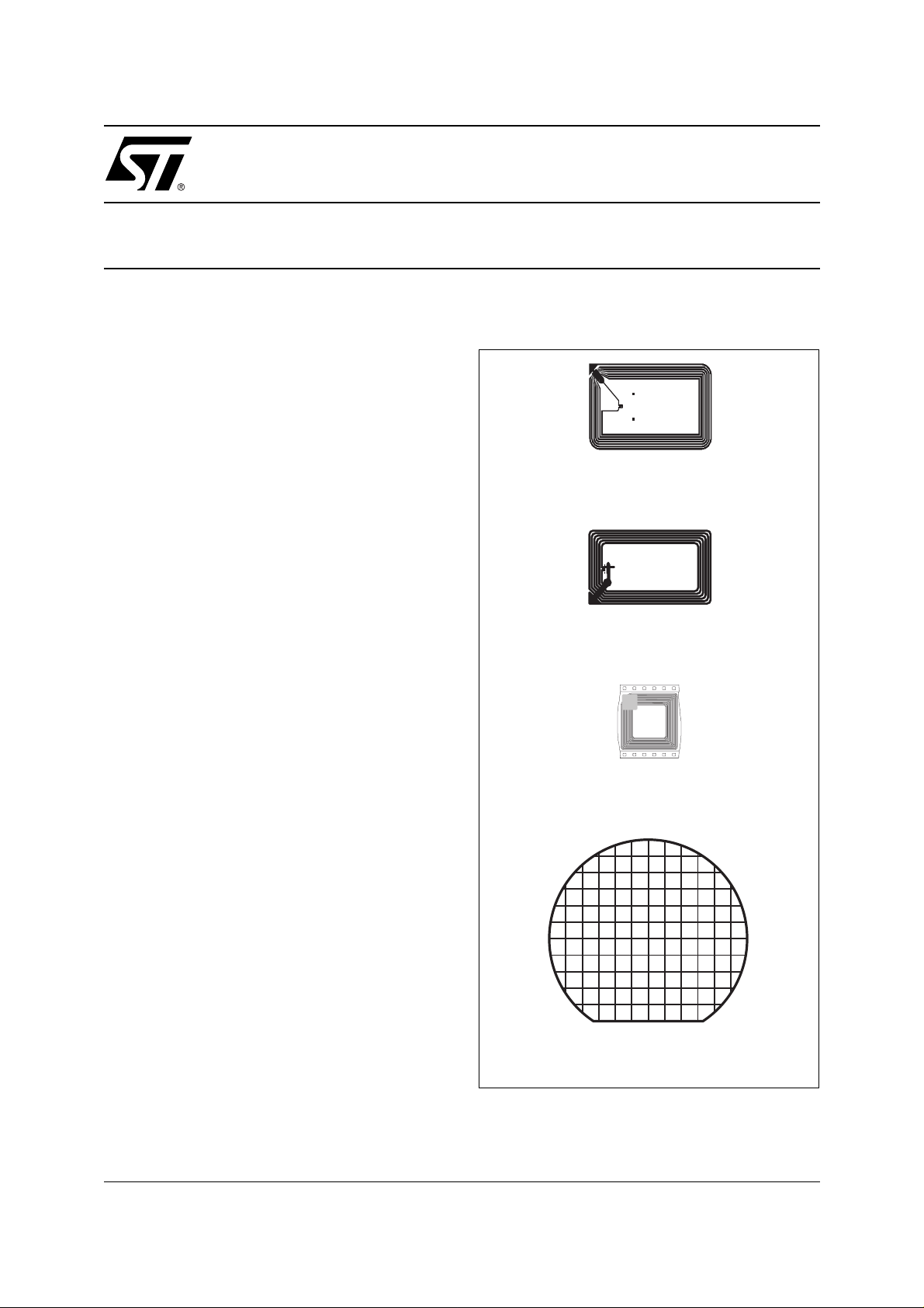
Figure 1. Delivery Forms
Antenna
(A1T/ISOR, A1S/I SOR)
Antenna
(A2T/ISOK)
Antenna
(C40)
Wafer
1/54July 2002
Page 2
LRI512
SUMMARY DESCRIPTION
The LRI512 is a contactless memory, powered by
an externally transmitted radio wave. It is fully
compliant with the ISO15693 recomm enda tion for
radio-frequency power and signal interface.
The LRI512 contains 512 bits of Electrically
Erasa ble Prog rammabl e Memory (EEPRO M). The
memory is organized as 16 blocks of 32 bits.
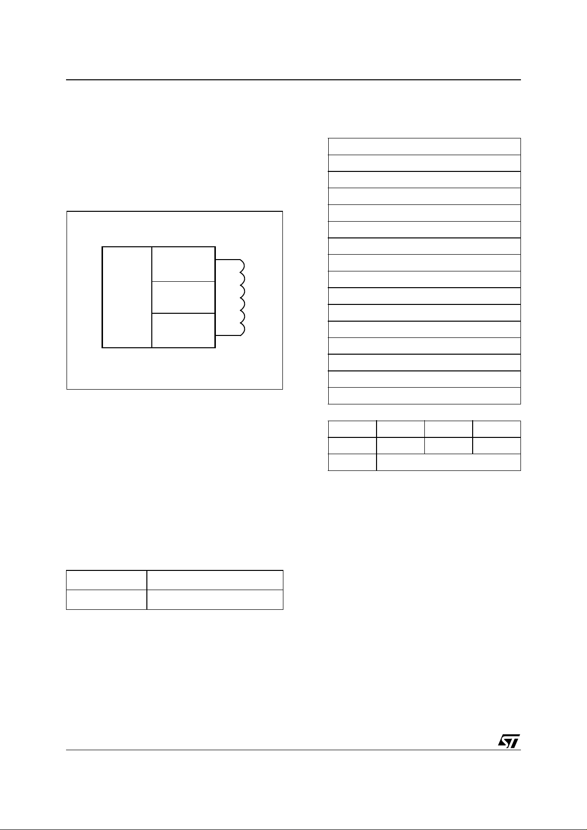
Figure 2. Logic Diagram
LRI512
AC1
AC0
512 bit
EEPROM
Power
Supply
Regulator
ASK
Demodulator
Manchester
Load
Modulator
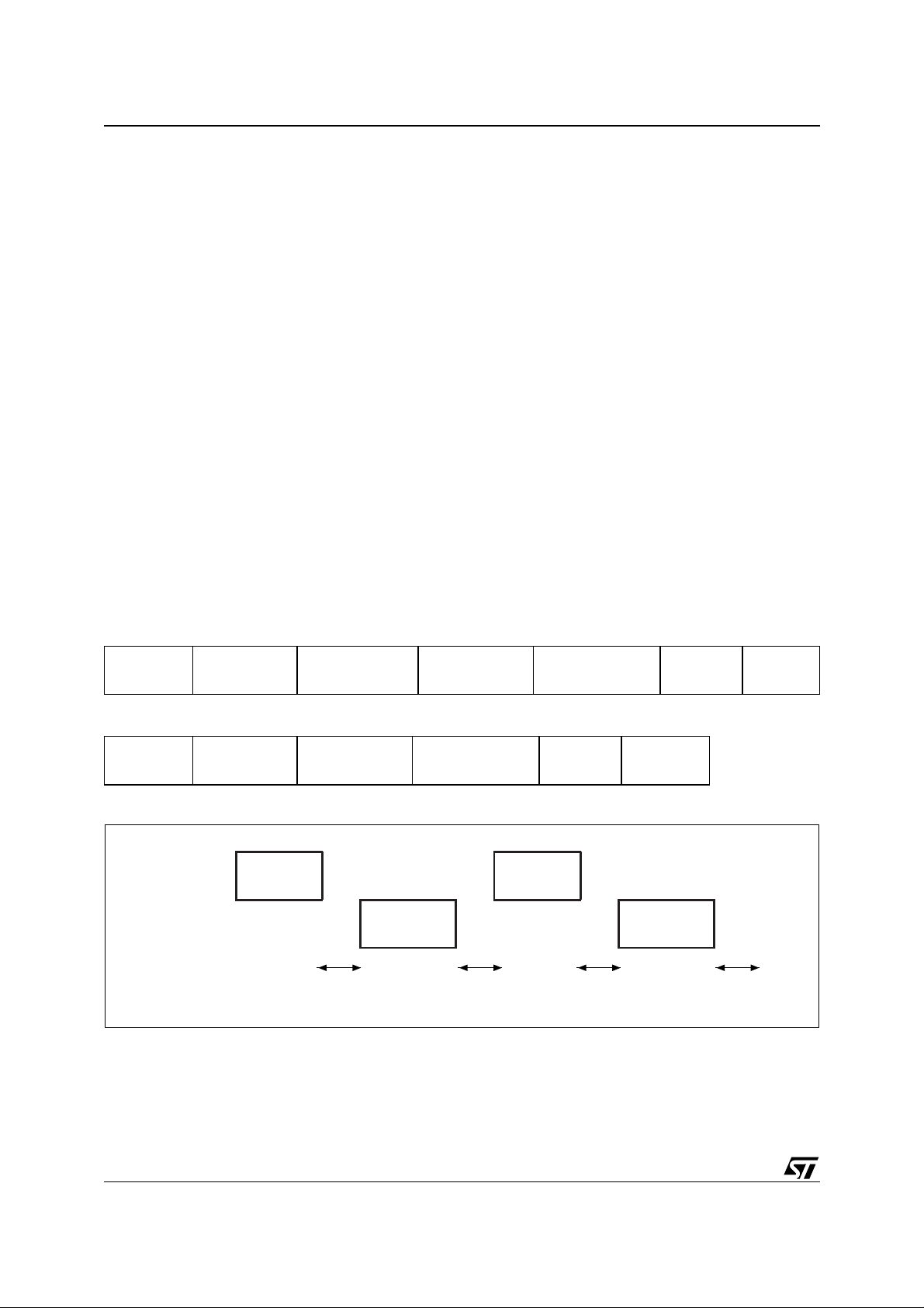
Table 2. LRI512 Memory Map
Addr 0 7 8 15 16 23 24 31
0 User Area
1 User Area
2 User Area
3 User Area
4 User Area
5 User Area
6 User Area
7 User Area
8 User Area
9 User Area
10 User Area
11 User Area
12 User Area
13 User Area
AI04008B
The LRI512 is accessed by modulating the
13.56 MHz carrier frequency. Incoming data are
demodulated from the received signal amplitude
modulation (ASK, Amplitude Shift Keying). The
received ASK wave is 10% or 100% modulated
(amplitude modulation). The Data transfer rate is
1.6 kbit/s using the 1/256 pulse coding mod e and
26 kbit/s using the 1/4 pulse coding modes.
Outgoing data are generated by antenna load
variation, using the Manchester coding, using one
or two sub-carrier frequencies at 423 kHz and
484 kHz. The Data transfer rate is 6.6 kbit/s, in the
low data rate mode, and 26 kbit/s, in the fast data
rate mode.
Table 1. Signal Names
AC1 Antenna Coil
AC0 Antenna Coil
Memory Mapping
The LRI512 is divided in 16 blocks of 32 bits. Each
block can be individually Write Protected using a
specific Lock command.
14 User Area
15 User Area
UID 0 UID 1 UID 2 UID 3
UID 4 UID 5 UID 6 UID 7
AFI
The User Area consists of blocks that are always
accessible in READ. WRITE commands are possible if the addressed block is not locked. During a
WRITE, the 32 bits of the block are replaced by the
new 32-bit value.
The LRI512 also has a 64-bit block that is used to
store the 64-bit Unique Identifier (UID). This UID is
compliant to the ISO15963 description, and its value is used during the anti-collis ion sequence (INVENTORY). This block is not accessible by the
user, and the value is written by ST on the production line.
The LRI512 also has an AFI regist er in which the
Application Family Identifier is stored, for use in
the anti-collision algorithm.
2/54
Page 3

LRI512
Commands
The LRI512 supports the following commands:
INVENTORY
–
: used to perform the anti-collision
sequence.
–
STAY QUIET:
to put the LRI512 in quiet mode.
The LRI512 is then deselected and does not respond to any command.
SELECT:
–
used to select the LRI512. After this
command, the LRI512 processes all READ/
WRITE commands with the Select_Flag set.
–
RESET TO READY:
to put the LRI512 i n the
ready state.
–
READ BLOCK:
to output the 32 bits of the se-
lected block and its locking status.
–
WRITE BLOCK:
to write the 32-bit value in the
selected block, provided that it is not locked.
–
LOCK BLOCK:
to lock the select ed b lock. After
this command, the block cannot be modified.
–
WRITE AFI:
to write the 8-bit v alue in the AFI
register, provided that it is not locked.
–
LOCK AFI:
ACTIVATE EAS:
–
to lock the AFI register.
to set the non volatile EAS bit.
When the EAS b i t is set, th e L R I512 answers to
the POOL EAS command.
DEACTIVATE EAS:
–
to reset the non volatile
EAS bit, so that the LRI512 no longer answers
to the POOL EAS command.
POOL EAS
–
: used to request all LRI512s in the
Reader field to generate the EAS signal, provided that their EAS bit is set.
Initial Dialogue for Vicinity Cards
The dialogue between the Vicinity Coupling Device (VCD) and the Vicinity Integrated Circuit Card
(LRI512) is conducted through the following consecutive operations:
– activation of the LRI512 by the RF operating
field of the VCD.
– transmission of a command by the VCD.
– transmission of a response by the LRI512.
These operations use t he RF power transfer and
communication signal interface specified in the following paragraphs. This technique is called Reader Talk First (RTF).
Power Transfer
Power transfer to the LRI512 is accomplished by
radio frequency at 13.56 MHz via coupling antennas in the LRI512 and in the VCD. The RF operating field of the VCD i s t ransformed on the LRI512
antenna as an AC voltage which is re-dressed, filtered and internally regulated. The amplitude
modulation (ASK) on this received signal is demodulated by the ASK demodulator.
Frequency
The ISO15693 standard defines the carrier fre-
f
quency (
) of the operating field to be
c
13.56 MHz ± 7 kHz.
Operating Fi e l d
The LRI512 operates continuously bet ween H
and H
– The minimum operating f ield is H
max
.
and has a
min
min
value of 150 mA/m rms.
– The maximum operating field is H
and has a
max
value of 5 A/m rms.
A VCD shall generate a field of at lea st H
not exceeding H
in the operating volume.
max
min
and
3/54
Page 4
LRI512
COMMUNICATION SIGNAL FROM VCD TO LRI512
Since the LRI512 is fully compliant with the
ISO15693 recommendat ion, the descriptions and
illustrat ions that follow are very he avily based on
those of the ISO/IEC documents: ISO/IEC 156932:2000(E) and ISO/IEC 15693-3:2001(E). This
has been done with the kind permission of the ISO
Copyright Office.
Communications between the VCD and the
LRI512 takes place using the modulation principle
of ASK (amplitude modulation). Two modulation
indices are used, 10% and 100%. The LRI512 decodes both. The VCD determines which index is
used.
The modulation index is defined as [a-b]/[a+b]
where a and b are the peak and minimum signal
amplitude, respectively, of the carrier frequency.
Depending of the choice made by the VCD, a
“pause” will be created as desc ribed in Figure 3
and Figure 4.
The LRI512 is operational for any de gree of m odulation index from between 10% and 30%.
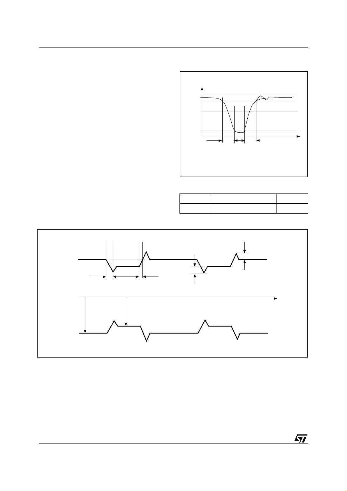
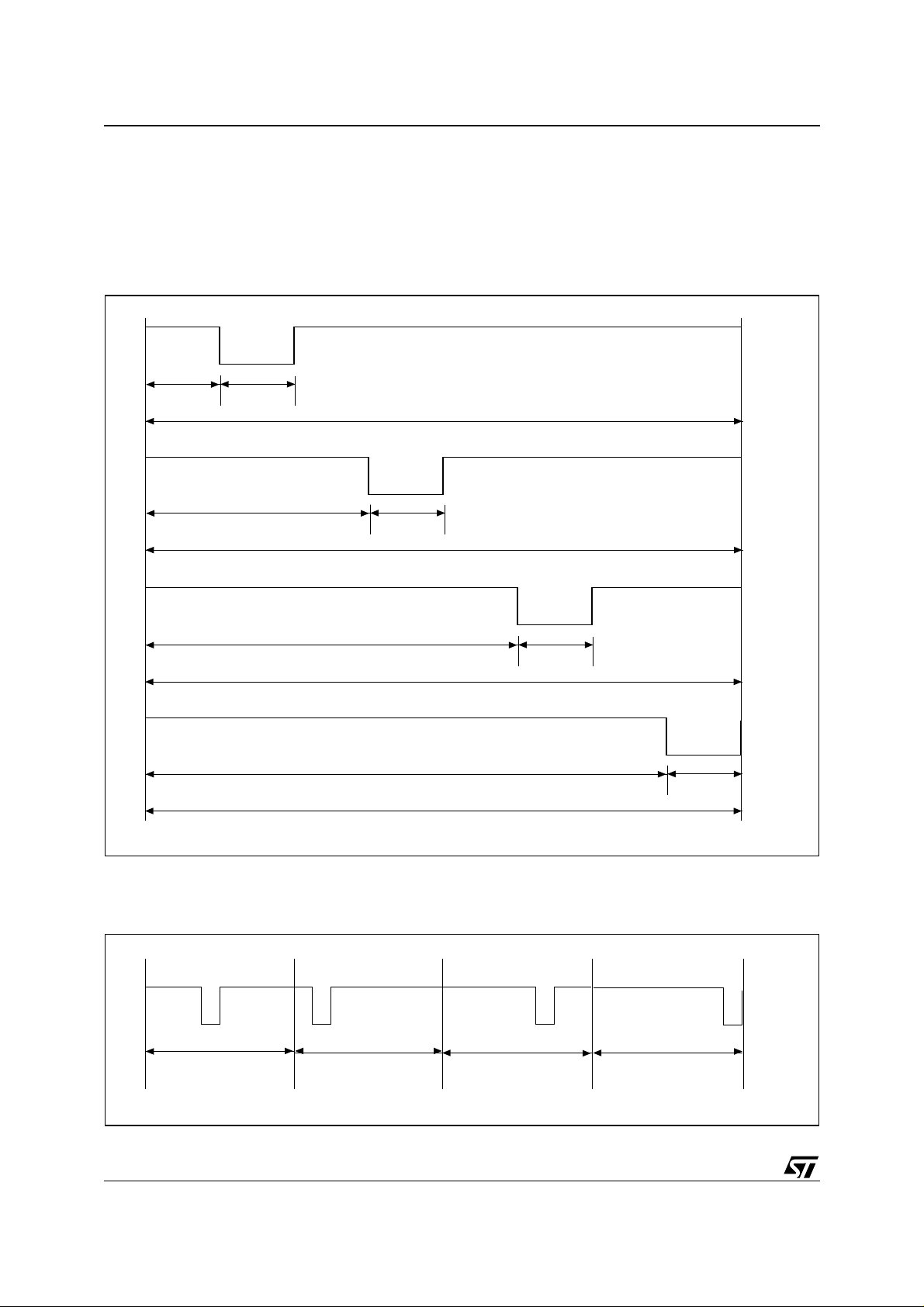
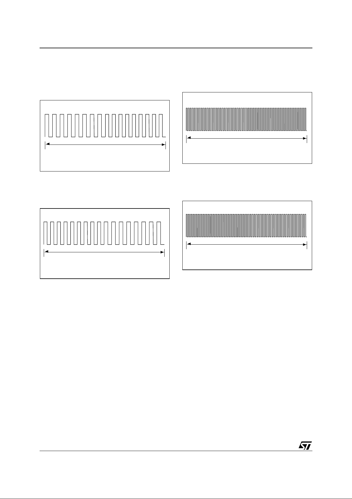
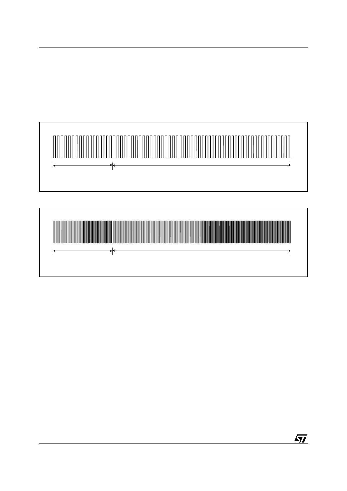
Figure 3. 100% Modulation Waveform
a
105%
100%
95%
60%
5%
tRFF
tRFR
tRFSBL
Table 3. 10% Modulation Parameters
hr 0.1 x (a-b) max
hf 0.1 x (a-b) max
t
AI06683
Figure 4. 10% Modulation Waveform
tRFF tRFSFL tRFR
ab t
hf
hr
AI06655
4/54
Page 5
DATA RATE AND DATA CODING
The data coding implemented in the LRI512 uses
pulse position modulation. Both data coding
modes that are described in the ISO15693 are
supported by the LRI512. The sel ection is made
by the VCD and indicated to the LRI512 within the
Start of Frame (SOF).
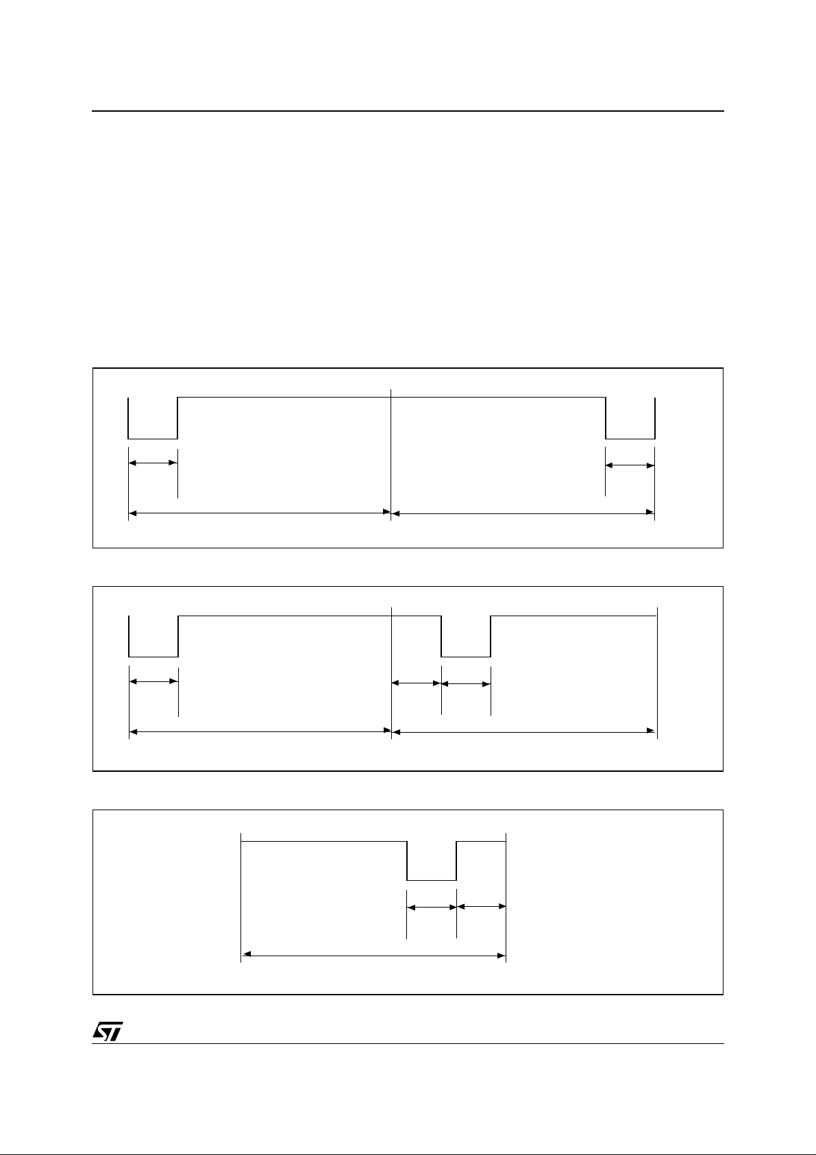
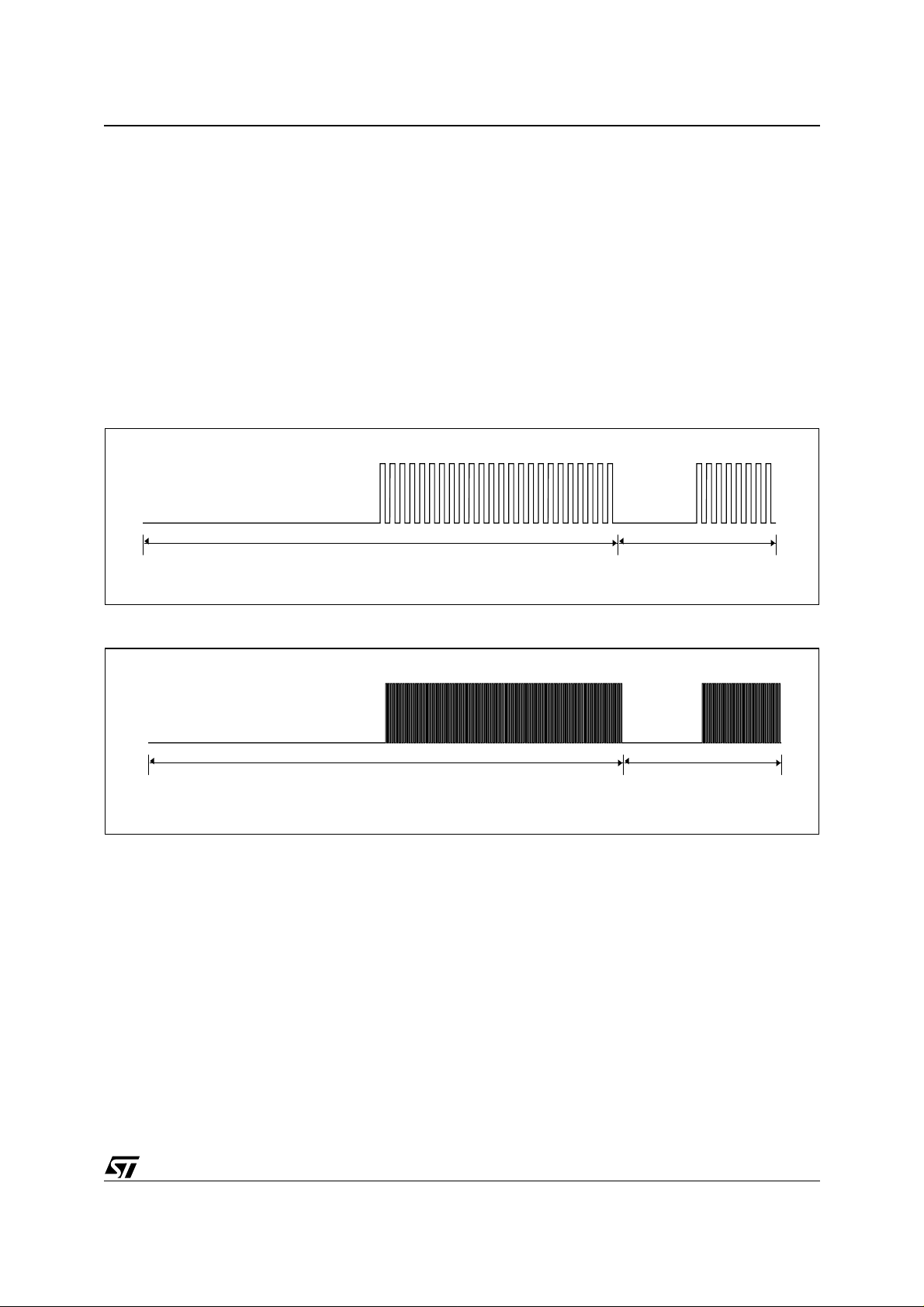
Data Coding Mode: 1 Out of 256
The value of one single byte is represented by the
position of one pause. Th e position of the pause
on 1 of 256 successive time period s of 18.88 µs
(256/f
), determines the value of the byte. In this
C
Figure 5. 1 Out of 256 Codin g Mode
Pulse
Modulated
Carrier
LRI512
case the transmission of one byte takes 4.833 ms
and the resulting data rate is 1.65 kbit/s (f
Figure 5 illustr ates t his puls e pos ition mo dulat ion
technique. In this figure, data E1h (225d) is sent by
the VCD to the LRI512.
The pause shall occur during the second half of
the position of the t ime pe riod t hat de term ines the
value, as shown in Figure 6.
A pause during the first period transmit the data
value 00h. A pause during the last period transmits
the data value FFh (255d).
9.44 µs
18.88 µs
/8192).
C
0 1 2 3 . . . . . . . . 2 . . . . . . . . . . . . . . . . . . . . . 2 2 2 2
. . . . . . . . . 2 . . . . . . . . . . . . . . . . . . . . . 5 5 5 5
. . . . . . . . . 5 . . . . . . . . . . . . . . . . . . . . . 2 3 4 5
Figure 6. Detai l of One Time Period
Pulse
Modulated
Carrier
4.833 ms
AI06656
9.44 µs
18.88 µs
. . . . . . .. . . . . . .
2
2
4
2
2
5
2
2
6
Time Period
one of 256
AI06657
5/54
Page 6
LRI512
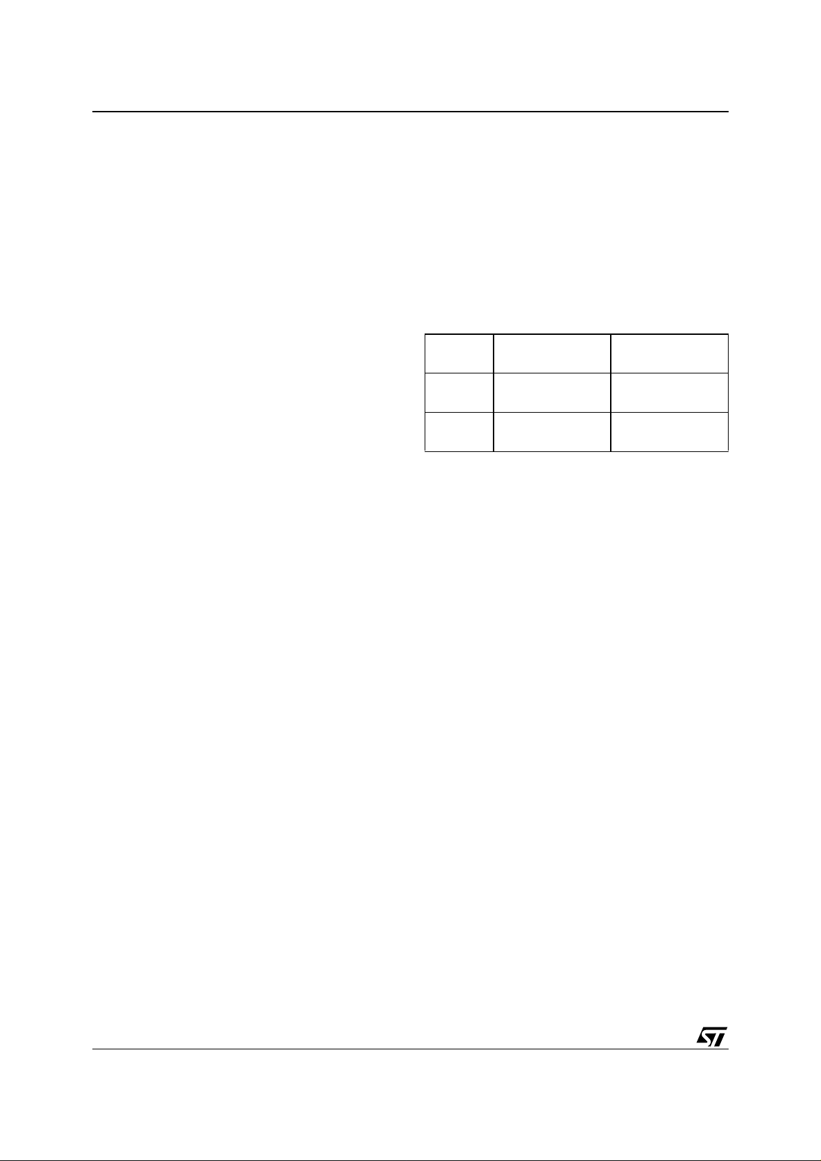
Data Coding Mode: 1 Out of 4
The value of 2 bits is represented by the position
of one pause. The position of the pause on 1 of 4
successive time periods of 18.88 µs (256/f
), de-
C
termines the value of the 2 bi ts. Four succes sive
Figure 7. 1 Out of 4 Coding Mode
Pulse position for "00"
9.44 µs 9.44 µs
Pulse position for "01" (1=LSB)
28.32 µs 9.44 µs
Pulse position for "10" (0=LSB)
pairs of bits form a byte, where the least significant
pair of bits is transmitted first.
In this case the transmission of one byte takes
302.08 µs and the resulting data rate is 26.48 kbit/
/512). Fig ure 7 illustr ates the 1 out o f 4 pulse
s (f
C
position technique and coding.
75.52 µs
75.52 µs
Pulse position for "11"
For example Figure 8 shows the transmission of
E1h (225d, 1110 0001b) by the VCD.
Figure 8. 1 Out of 4 Coding Exampl e
10
75.52 µs
00
75.52 µs
47.20µs 9.44 µs
75.52 µs
66.08 µs 9.44 µs
75.52 µs
AI06658
01 11
75.52 µs 75.52 µs
AI06659
6/54
Page 7
LRI512
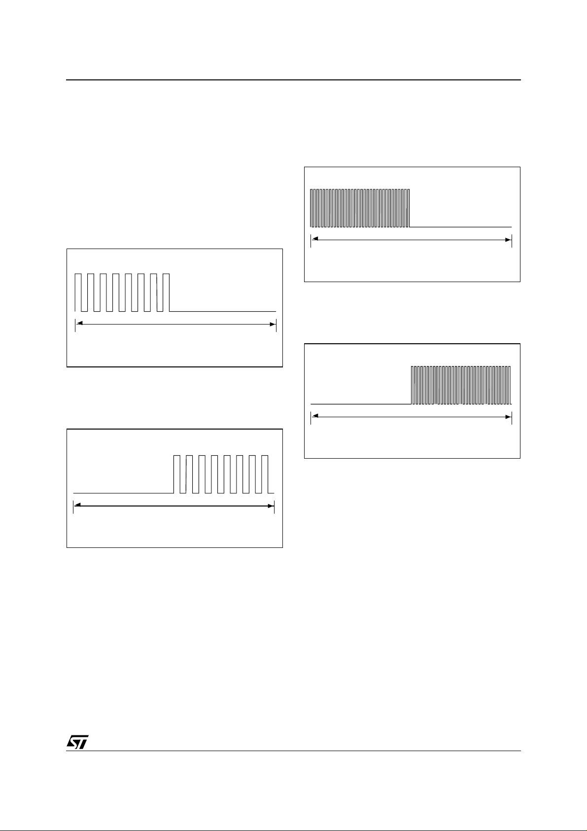
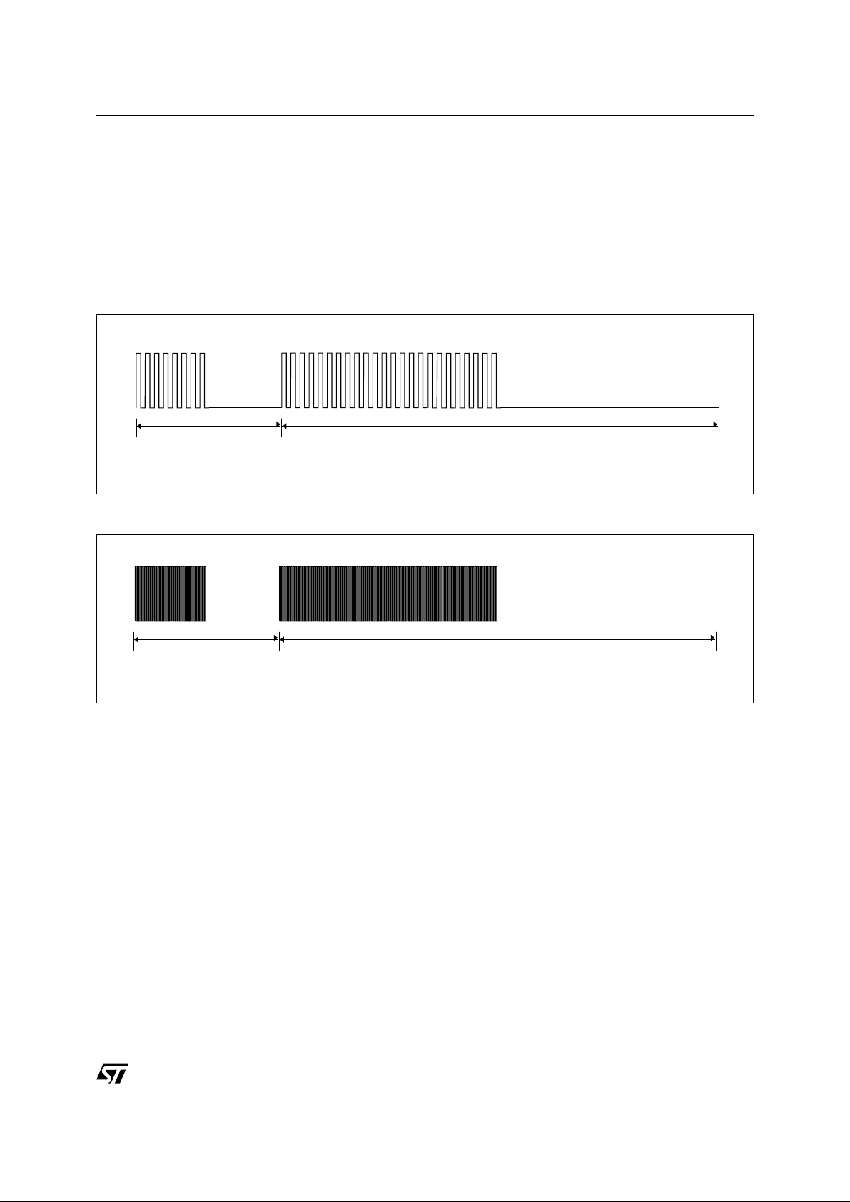
VCD to LRI512 Frames
Frames are delimited by a Start of Frame (SOF)
and an End of Frame (EOF) and are implemented
using code violation. Unused options are reserved
for fu tu r e u s e .
The LRI512 is ready to receive a new command
frame from the VCD after a delay of t
after having
2
sent a response frame to the VCD (as specified in
Table 59).
The LRI512 generates a Power-on delay of t
MINCD
after being activated by the powering field (as
specified in Table 59). After this delay, the LRI512
is ready to receive command frames from the
VCD.
Start of Frame (SOF)
The SOF defines the data codi ng mode the V CD
is to use for the following command frame.
The SOF sequence described in Figure 9 selects
the 1 out of 256 data coding mode.
The SOF sequence described in Figure 10 selects
the 1 out of 4 data coding mode.
The EOF sequence for either coding mode is described in Figure 11.
Figure 9. SOF to Select 1 Out of 256 Data Coding Mode
9.44 µs
37.76 µs
37.76 µs
9.44 µs
AI06661
Figure 10. SOF to Select 1 Out of 4 Data Coding Mode
9.44 µs
37.76 µs
9.44 µs
Figure 11. EOF for Either Data Co ding Mod e
9.44 µs
37.76 µs
9.44 µs
9.44 µs
37.76 µs
AI06660
AI06662
7/54
Page 8
LRI512
COMMUNICATIONS SIGNAL FROM LRI512 TO VCD
For some parameters several modes have been
defined in order to allow for use in different noise
environments and application requirements.
Load Modulation
The LRI512 is capable of communication to the
VCD via an inductive couplin g area in which the
carrier is loaded to generate a s ubcarrier with frequency f
ing in a load in the LRI512.
Subcarri er
The LRI512 supports the one subcarrier and two
subcarriers response formats. These formats are
selected by the VCD using the first bit in the protocol header.
When one subcarrier is used, the frequency f
the subcarrier load m odulation is 423.75kHz ( f
32).
When two subcarriers are used, the frequency f
is 423.75 kHz (f
484.28 kHz (f
. The subcarrier is generated by switch-
S
S
/32), and the frequency fS2 is
C
/28). When using the two subcarri-
C
1 of
C
S
/
1
ers mode, the LRI512 generates a continuous
phase relationship between f
1 and fS2.
S
Data Rates
The LRI512 can respond using the low or the high
data rate format. The selection of the data rate is
made by the VCD using the s econd bi t in t he protocol header.
Table 4 shows the different data rates the LRI512
can achieve using each combination.
Table 4. Response Data Rate
Data Rate One Subcarrier Two Subcarriers
Low
High
6.62 kbit/s
/2048)
(f
C
26.48 kbit/s
/512)
(f
C
6.67 kbit/s
(fC/2032)
26.69 kbit/s
(fC/508)
8/54
Page 9
BIT REPRESENTATION AND CODING
Data bits are encoded usin g Manchester coding,
according to the following schemes.
For the low data rate the same subcarrier frequency or frequencies are used, in this case the num ber of pulses shall be multiplied by 4 and all times
will increas e b y thi s fa cto r .
Bit Coding Using One Subcarrier
High Data Rate. A logic 0 starts with 8 pulses of
423.75 kHz (f
/32) followed by an unmodulated
C
time of 18,88µs as shown in Figure 12.
LRI512
Low Data Rate. A logic 0 starts with 32 pulses of
423.75 kHz (fC/32) followed by an unmodulated
time of 75.52 µs as shown in Figure 14.
Figure 14. Logi c 0, Lo w D ata Ra te
Figure 12. Lo gi c 0 , Hi gh D at a R at e
37.76 µs
AI06663
A logic 1 starts with an unmodulated time of
18.88 µ s followed by 8 pulses of 423.75 kHz (f
C
32) as shown in Figure 13.
Figure 13. Lo gi c 1 , Hi gh D at a R at e
37.76 µs
AI06664
149.86 µs (ISO=151.04 µs)
A logic 1 starts with an unmodulated time of
75.52 µ s followed by 32 pulses of 423.75 kHz (f
32) as shown in Figure 15.
Figure 15. Logi c 1, Lo w D ata Ra te
/
149.86 µs (ISO=151.04 µs)
AI06666
AI06665
/
C
9/54
Page 10
LRI512
Bit Coding Usi ng Two Subcarri ers
High Data Rate. A logic 0 starts with 8 pulses of
423.75 kHz (f
484.28 kHz (f
/32) followed by 9 pulses of
C
/28) as shown in Figure 16.
C
Figure 16. Lo gi c 0, Hi gh D a ta Ra te
37.46 µs
AI06670
A logic 1 starts with 9 pulses of 484.28 kHz (f
followed by 8 pulses of 423.75 kHz (f
C
/32) as
C
/28)
shown in Figure 17.
Figure 17. Lo gi c 1 , Hi gh D at a R at e
Low Data Rate. A logic 0 starts with 32 pulses of
423.75 kHz (f
484.28 kHz (f
/32) followed by 36 pulses of
C
/28) as shown in Figure 18.
C
Figure 18. Logic 0, Low Data Rate
149.86 µs ± 0.3 µs
AI06668
A logic 1 starts with 36 pulses of 484.28 k Hz (f
28) followed by 32 pulses of 423.75 kHz (f
/32) as
C
C
shown in Figure 19.
Figure 19. Logic 1, Low Data Ra te
/
37.46 µs
149.86 µs ± 0.3 µs
AI06667
AI06669
10/54
Page 11
LRI512 TO VCD FRAMES
Frames are delimited by an SOF and EOF and are
implemented using code violation. Unused options
are reserved for future use.
For the low data rate, the same subcarrier frequency or frequencies are used. In this case the
number of pulses shall be multiplied by 4.
The VCD is ready to receive a response frame
from the LRI512 w ithin less than t
after having
1
sent a command frame (as specified in Table 59).
SOF Wh en U si ng One Subcarri er
High Data Rate. SOF comprises 3 parts: (see
Figure 20)
– an unmodulated time of 56.64 µs,
– 24 pulses of 423.75 kHz (
– a logic 1 which starts with an unmodulated time
of 18.88 µs followed by 8 pulses of 423.75 kHz.
Low Data Rate. SOF comprises 3 parts: (see
Figure 21)
– an unmodulated time of 226.56 µs,
– 96 pulses of 423.75 kHz (
– a logic 1 which starts with an unmodulated time
of 75.52 µs followed by 32 pulses of
423.75 kHz.
Figure 20. Start of Frame, High Data Rate, One Subcarrier
113.28 µs 37.76 µs
f
c
f
c
LRI512
/32),
/32),
AI06671
Figure 21. Start of Frame, Low Data Rate, One Subcarrier
453.12 µs 149.86 µs (ISO=151.04 µs)
AI06672
11/54
Page 12
LRI512
SOF When U si ng Two Subcarri er s
High Data Rate. SOF comprises 3 parts: (see
Figure 22)
f
– 27 pulses of 484.28 kHz (
– 24 pulses of 423.75 kHz (
c
f
c
/28),
/32),
– a logic 1 which starts with 9 pulses of
484.28 kHz followed by 8 pulses of 423.75 kHz.
Low Data Rate. SOF comprises 3 parts: (see
Figure 23)
– 108 pulses of 484.28 kHz (
– 96 pulses of 423.75 kHz (
– a logic 1 which starts with 36 pulses of
484.28 kHz followed by 32 pulses of
423.75 kHz.
Figure 22. Start of Frame, High Data Rate, Two Subcarriers
112.39 µs 37.76 µs (ISO=37.46 µs)
Figure 23. Start of Frame, Low Data Rate, Two Subcarriers
f
c
f
/28),
c
/32),
AI06673
449.56 µs
149.86 µs ± 0.3 µs
AI06674
12/54
Page 13
LRI512
EOF When Us i ng On e Su bc arrier
High Data Rate. EOF comprises 3 parts: (see
Figure 24)
– a logic 0 which starts with 8 pulses of
423.75 kHz followed by an unmodulated time of
18.88 µs.
f
– 24 pulses of 423.75 kHz (
/32),
c
Low Data Rate. EOF comprises 3 parts: (see
Figure 25)
– a logic 0 which starts with 32 pulses of
423.75 kHz followed by an unmodulated time of
75.52 µs.
– 96 pulses of 423.75 kHz (
– an unmodulated time of 226.56 µs.
– an unmodulated time of 56.64 µs.
Figure 24. End of Frame, High Data Rate, One Subcarrier
37.76 µs
Figure 25. End of Frame, Low Data Rate, One Subcarrier
113.28 µs
f
c
/32),
AI06675
453.12 µs151.04 µs
AI06676
13/54
Page 14
LRI512
EOF When U si ng Two Subcarri er s
High Data Rate. EOF comprises 3 parts: (see
Figure 26)
– a logic 0 which starts with 8 pulses of
423.75 kHz followed by 9 pulses of 484.28 kHz,
– 24 pulses of 423.75 kHz (
– 27 pulses of 484.28 kHz (
f
c
f
c
/32),
/28).
Low Data Rate. EOF comprises 3 parts: (see
Figure 27)
– a logic 0 which starts with 32 pulses of
423.75 kHz followed by 36 pulses of
484.28 kHz,
– 96 pulses of 423.75 kHz (
– 108 pulses of 484.28 kHz (
Figure 26. End of Frame, High Data Rate, Two Subcarriers
112.39 µs37.46 µs
Figure 27. End of Frame, Low Data Rate, Tw o S ubcar riers
f
c
/32),
f
/28).
c
AI06677
449.56 µs151.62 µs (ISO=149.86 µs)
AI06678
14/54
Page 15
UNIQUE IDENTIFIER (UID)
The LRI512s are uniquely identified by a 64-bit
Unique Identifier (UID). This UID complies with
ISO/IEC 15963 and ISO/IEC 7816-6. The UID is a
read only code, and comprises:
– The 8 MSB is E0h
– The IC Ma nufacturer code of ST 02h, o n 8 bits
(ISO/IEC 7816-6/AM1)
– A Unique Serial Number on 48 bits.
The UID is used for addressing each LRI512
uniquely and individu ally, during the ant i-collision
APPLICATION FAMILY IDENTIFIER (AFI)
The AFI (Application Family Identifier) describes
the type of application targeted by the VCD, and is
used to extract from all the LRI512 s present only
the LRI512s meeting the required application criteria .
It is programmed by the LRI512 issuer in the AFI
register. Once programmed and Locked, it cannot
be modified.
The most significant ni bble of A FI i s used to code
one specific or all application families.
The least significant nibble of AFI i s used to code
one specific or all application sub-families. Subfamily codes, other than 0, are proprietary.
(See ISO 15693-3 documentation)
LRI512
loop and for one-to-one exchange between a VCD
and a LRI512.
Table 5. UID Format
MSB LSB
63 56 55 48 47 0
E0h 02h Unique Serial Number
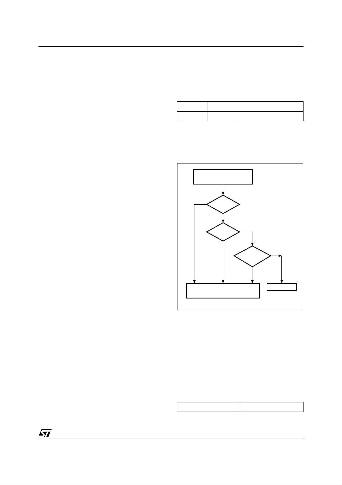
Figure 28. LRI512 Decision Tree for AFI
Inventory Request
Received
No
AFI Flag
Set ?
Yes
AFI value
= 0 ?
Yes
No
AFI value
= Internal
value ?
No
CRC
The CRC used in the LRI512 is calculated as per
the definition in ISO/IEC 13239.
The initial register content is all ones: FFFFh.
The 2-byte CRC is appended to each Request and
each Response, within each frame, before the
EOF. The CRC is calculated on all the bytes after
the SOF up to the CRC field.
Upon reception of a Request from the VCD, the
LRI512 verifies that the CRC value is valid. If it is
invalid, it discards the frame, and does not answer
the VCD.
Upon reception of a Response from the LRI512, it
is recommended that the VCD verify that the CRC
Yes
Answer given by the LRI512
to the Inventory Request
No Answer
AI06679
value is valid. If it is invalid, actions to be performed are left to the responsibility of the VCD designer.
The CRC is transmitted Least Significant Byte first.
Each byte is transmitted Least Significant Bit first.
Table 6. CRC Transmission Rules
LSByte MSByte
LSBit MSBit LSBit MSBit
CRC 16 (8bits) CRC 16 (8 bits)
15/54
Page 16
LRI512
LRI512 PROTOCOL DESCRIPTI ON
The Transmission protocol defines the mechanism to exchange instructions and data between
the VCD and the LRI512, in both directions.
It is based on the concept of “VCD talks first”.
This means that any LRI51 2 does n ot start trans-
mitting unless it has received and properly decoded an instruction sent by the VCD.
The protocol is based on an exchange of
– a Request from the VCD to the LRI512
– a Response from the LRI512 to the VCD
Each Request and each Response is contained in
a Frame. The frame delimiters (SOF, EOF) are described in the previous paragraphs.
Each Request consists of
– Request SOF (see Figure 9 and Figure 10)
– Flags
– A Command Code
– Parameters, depending on the Command
– Application data
– 2-byte CRC
– Request EOF (see Figure 11)
Each Response consists of
– Answer SOF (see Figure 20 to Figure 23)
– Flags
– Parameters, depending on the Command
– Application data
– 2-byte CRC
– Answer EOF (see Figure 24 to Figure 27)
The protocol is bit-oriented. The number of bits
transmitted in a frame is a multiple o f eight (8) –
that is, an integer number of bytes.
A single-byte field is transm itted Least Significant
Bit (LSBit) first.
A multiple-byte field is transmitted Least Significant Byte (LSByte) first, each byte is transmitted
Least Significant Bit (LSBit) first.
The setting of the flags indicates the pres ence of
the optional fields. When the flag is s et (to one),
the field is present. When the flag is reset (to zero),
the field is absent.
Table 7. VCD Request Frame Format
Request
SOF
Request Flags Command Code Parameters Data
Table 8. LRI512 Response Fr ame Fo rm at
Response
SOF
Response
Flags
Parameters Data
Figure 29. LRI512 Protocol Timing
VCD
LRI512
Timing
Request Frame
(Table 7)
Response Frame
(Table 8)
t1 t2 t1 t2
2 Bytes
CRC
Request Frame
(Table 7)
2 Bytes
CRC
Response
EOF
Response Frame
(Table 8)
Request
EOF
AI06830
16/54
Page 17
LRI512 STATES
A LRI512 can be in one of four states:
– Power-off
– Ready
– Quiet
–Selected
Transitions between these s tates are specified in
Figure 30 and Table 9.
Power-off State
The LRI512 is in t he Power-of f state when it does
not receive enough energy from the VCD.
Quiet State
When in the Quiet State, the LRI512 answe rs any
Request other than an Inventory Request with the
Address_Flag set.
Selected State
In the Selected State, the LR I512 answers to any
Request in all modes:
– Request in Select mode with the Select flag set
– Request in Addressed mode if the UID match.
– Request in Non-Addressed mode as it is gener-
al Request.
Ready State
The LRI512 is in the Ready state when it receives
enough energy from the V CD. It sha ll ans wer any
Request where the Select_Flag is not set.
Table 9. LRI512 Response, Depending on the States of the Request Flags
Address_Flag Select_Flag
Flags
LRI512 in Ready or Selected state (Devices
in Quiet state do not answer)
LRI512 in Selected state X X
1
Addressed0Non Addressed
XX
Selected
LRI512
1
0
Non Selected
LRI512 in Ready, Quiet or Selected state (the
device which match the UID)
Error (03h) X X
XX
17/54
Page 18

LRI512
Figure 30. LRI512 State Transition Diagram
Out of field
Power Off
In field
Ready
Out of field
Stay quiet(UID)
Reset to ready
Select (UID)
Quiet
Any other command where the
Address_Flag is set AND
where Inventory_Flag is not set
Note: The intention of the state transition method is that only one LRI512 should be in the selected state at a time.
Any other Command
where Select_Flag
is not set
Select (UID)
Reset to ready where
Select_Flag is set or
Select(different UID)
Stay quiet(UID)
Any other command
Selected
Out of field
AI06681
18/54
Page 19

MODES
The set of LRI512s that can answer a given Re-
quest are those whose current “Mode” is the appropriate one for that request.
Addressed Mode
When the Address_flag is set to 1 (addressed
mode), the Request shall cont ain the Unique ID
(UID) of the addressed LRI512.
Any LRI512 receiving a Request with the
Address_flag set to 1 shall compare the received
Unique ID to its own UID.
If it matches, it shall execute it (if possible) and return a Response to the VCD as specified by the
command description.
If it does not match, it shall remain silent.
Non-Addressed mode (General Request)
When the Address_flag is set to 0 (non-addressed
mode), the Request shall not contain a Unique ID.
LRI512
Any LRI512 receiving a Request with the
Address_flag set to 0 executes it and returns a Response to the VCD as specified by the command
description.
Select Mode
When the Select_flag is set to 1 (select mode), the
Request shall not contain a LRI512 Unique ID.
The LRI512 in the Selected State receiving a Request with the Select_flag set to 1 executes it and
returns a Response to the VCD as specified by the
command description.
Only LRI512s in the Selected State answer to a
Request having the Select Flag set to 1.
The system design ensures in theory that only one
LRI512 can be in the Select state.
19/54
Page 20

LRI512
REQUEST FORMAT
The Request consists of
–SOF
– Flags
– A Command Code
– Parameters and Data
– CRC
–EOF
Table 10. General Request Format
S
Request
O
Flags
F
Request Flags
In a Request, the flags field specifies the actions to
be performed by the LRI512, and whe ther corresponding fields are present or not.
It consists of eight bits.
The bit 3 (Inventory_flag) of the request flag de-
fines the content of the 4 MSBs (bits 5 to 8).
When bit 3 is reset (0), bits 5 to 8 define the
LRI512 selection criteria.
When bit 3 is set (1), bits 5 to 8 define the LRI512
Inventory parameters.
Table 11. Request Flags 1 to 4 Definition
Bit 1
Bit 2
Command
Sub-carrier
flag
Data_rate
flag
Code
Parameters Data CRCEO
A single sub-carrier frequency
0
shall be used by the LRI512
Two sub-carriers shall be used
1
by the LRI512
0 Low data rate is used
1 High data rate is used
Table 12. Request Flags 5 to 8 when Bit 3 = 0
Request shall be executed by
0
any LRI512 according to the
Bit 5 Select flag
Bit 6
F
Bit 7 Option flag 0
Bit 8 RFU 0
Note: if the Select_flag is set to 1, the Address_flag shall be set to
Address
flag
0 and the UID field shall not be present in the Request.
setting of Address_flag
Request shall be executed only
1
by LRI512 in Selected State
Request is not addressed. UID
0
field is not present. It shall be
executed by all LRI512.
Request is addressed. UID field
is present. It shall be executed
1
only by the LRI512 whose UID
matches the UID specified in
the Request.
Table 13. Request Flags 5 to 8 when Bit 3 = 1
Bit 5 AFI flag
Bit 6 Nb_slots flag
Bit 7 Option flag 0
Bit 8 RFU 0
0 AFI field is not present
1 AFI field is present
0 16 slots
1 1 slot
Flags 5 to 8 meaning are
0
Inventory
Bit 3
Bit 4
Note: 1. Sub-carrier_flag refers to the LRI512-to-VCD communi-
20/54
flag
Protocol
Extension
flag
cation .
2. Data_rate_flag refers to the LRI512-to-VCD communication
according to Table 12
Flags 5 to 8 meaning are
1
according to Table 13
0 No Protocol format extension
Page 21

RESPONSE FORMAT
The Response consists of
–SOF
– Flags
– Parameters and Data
– CRC
–EOF
Table 14. General Response Format
Response
SOF
Flags
Parameters Data CRC EOF
Response Flags
In a Response, the f lags field indicates how actions have been performed by the LRI512 and
whether corresponding fields are present or not. It
consists of eight bits.
Table 15. Response Flags 1 to 8 definition
0 No error
Bit 1 Error flag
Error detected. Error code is
1
in the “Error” field.
LRI512
Response Error Code
If the Error Flag is set by the LRI512 in the Response, the Error Code field is present and provides information about the error that occurred.
The following error codes are specified. Other
codes are reserved for future use.
Table 16. Response Error Code Definition
Error
Code
03h The option is not supported
10h The specified block is not available
The specified block is already locked and thus
11h
cannot be locked again
The specified block is locked and its content
12h
cannot be changed.
Meaning
Bit 2 RFU 0
Bit 3 RFU 0
Extension
Bit 4
Bit 5 RFU 0
Bit 6 RFU 0
Bit 7 RFU 0
Bit 8 RFU 0
flag
0 No extension
21/54
Page 22

LRI512
ANTI-COLLISION
The purpose of the anti-collision sequence is to inventory the LRI512s pre sent in the VCD field by
their unique ID (UID).
The VCD is the master of the communication with
one or multiple LRI512s. It initiates LRI512 communication by issuing the Inventory Request.
The LRI512 sends its Res ponse in the slo t determined, or might not respond.
Table 17. Inventory Request Format
MSB LSB
SOF
Request
Flags
8 bits 8 bits 8 bits 8 bits 0 to 8 bytes 16 bits
Command Optional AFI
Request param eters
When issuing the Inventory Command, the VCD
shall:
– set the Nb_slots_flag to the desired setting,
– add after the Command Field the Mask Length
and the Mask Value,
– The Mask Length is the number of significant
bits of the Mask Value.
– The Mask Value is contained in an integer num-
ber of bytes. The Mask Length indicates the
number of significant bits. LSB shall be transmitted first.
– If the Mask Length is not a multiple of 8 bits, the
Mask Value MSB shall b e padded with the required number of null bits (set to 0) so that the
Mask Value is contained in an integer number of
bytes.
– The next field starts on the next byte boundary.
Mask
Length
Mask Value CRC EOF
In the example of the Table 18 and Figure 3 1, the
Mask Length is 11 bits . The Mask Value MS B is
padded with five bits set to 0. The 11 bits Mask
plus the current slot number is compared to the
UID.
Table 18. Example of the Padding of a 11 bits
Mask Value
(b15) MSB LSB (b0)
0000 0 100 1100 1111
Pad 11 bits Mask Value
22/54
Page 23

Figure 31. Principle of Comparison between the Mask, Slot Number and UID
LRI512
Mask value received in the Inventory command 0000 0100 1100 1111b16 bits
The Mask value less the padding 0s is loaded
into the Tag comparator
The Slot counter is calculated
The Slot counter is concatened to the Mask value
Nb_slots_flags = 0 15 bits
The concatenated result is compared with
the least significant bits of the Tag UID.
xxxx xxxx..... xxxx xxxx x xxx xxxx xxxx xxxx 64 bits
The AFI field shall be present if the AFI_flag is set.
The pulse shall be generated according to the def-
inition of the EOF in ISO/IEC 15693-2.
The first slot starts immediately after the reception
of the Request EOF.
To switch to the next slot, the VCD sends an EOF.
UID
The following rules and restrictions apply:
– if no L RI512 answer is detected, t he VCD m ay
switch to the next slot by sending an EOF
– if one or more LRI512 answers are detected, the
VCD shall wait until the complete frame has
been received before sending an EOF for
switching to the next slot.
100 1100 1111b11 bits
LSBMSB
xxxxNb_slots_flags = 0 (16 slots), Slot Counter is 4 bits
xxxx 100 1100 1111
CompareBits ignore d
LSBMSB
LSBMSB
4 bits
LSBMSB
b
b0b63
b
AI06682
23/54
Page 24

LRI512
REQUEST PROCESSING BY THE LRI512
Upon reception of a valid Request, the LRI512
performs the following algorithm, where:
– NbS is the total number of slots (1 or 16)
– SN is the current slot number (0 to 15)
– LSB (value, n) function returns the n least signif-
icant bits of the value
– MSB (value, n ) function returns the n most sig-
nificant bits of the value
– “&” is the concatenation operator
– Slot_Frame is either a SOF or an EOF
SN = 0
if (Nb_ slots_fl ag)
then NbS = 1
SN_lengt h = 0
endif
else NbS = 16
SN_lengt h = 4
endif
label1:
if LSB( UID, SN_ length + Mask_l ength) =
LSB(SN,S N_length )&LSB( Mask,Mask _lengt h)
then answer to inve ntory req uest
endif
wait (S lot_Fram e)
if Slot _Frame = SOF
then Stop Anticollisio n
decode/p rocess re quest
exit
endif
if Slot _Frame = EOF
if SN < N bS-1
thenSN = SN + 1
goto la bel1
exit
endif
endif
EXPLANATION OF THE POSSIBLE CASES
Figure 32 summarizes the main possible cases
that can occur during an anti-collision sequence
when the slot number is 16.
The different steps are:
– The VCD sends an Inventory Request, in a
frame, terminated by an EOF. The number of
slots is 16.
– LRI512 #1 transmits its Response in Slot 0. It is
the on ly one to do s o, therefore no collis ion oc-
curs and its UID is received and registered by
the VCD;
– The VCD sends an E OF, meaning to switch to
the next slot.
– In slot 1, two LRI512s, #2 and #3, transmit their
Responses. This generates a collision. The
VCD records it, and remembers that a collision
was detected in Slot 1.
– The VCD sends an E OF, meaning to switch to
the next slot.
– In Slot 2, no LRI512 transmits a Response.
Therefore the VCD does not detect a LRI512
SOF and decides to switch to the next slot by
sending an EOF.
– In slot 3, there is another collision caused by
Responses from LRI512 #4 and #5
– The VCD then decid es to send a Request (for
instance a Read Block) to LRI512 #1, whose
UID was already correctly received.
– All LRI512s detect a SOF and exit the anti-colli-
sion sequence. They p ro cess this Requ es t and
since the Request is addressed to LRI512 #1,
only LRI512 #1 transmits its Response.
– All LRI512s are ready to receive another Re-
quest. If it is an Inventory command, the slot
numbering sequence restarts from 0.
Note: the decision to interrupt the anti-collision sequence is up to the VCD. It could have continued
to send EOFs until Slot 15 and then send the Request to LRI512 #1.
24/54
Page 25

Figure 32. Description of a Possible Anti-collision Sequence
LRI512
EOF
LRI512 1
Request to
Response
Response
from
LRI512 1
Response
4
2
Response
Response
5
Collision
No
Response
3
Collision
AI06831
Slot 0 Slot 1 Slot 2 Slot 3
EOF EOF EOF EOF SOF
Request
Inventory
VCD SOF
LRI512s
1
Response
No
collision
Timing t1 t2 t1 t2 t3 t1 t2 t1
Comment
Time
25/54
Page 26

LRI512
TIMING DEFINITION
: LRI512 Response Delay
t
1
is as defined in Table 19.
t
1
Upon detection of the rising edge of the EOF received from the VCD, the LRI 512 wait for a time
equal to
(typ) = 4352/fC (see Table 59)
t
1
before starting to transmit its response to a VCD
request or switch to the next slot when in an inventory process.
The EOF is defined in page 7.
: VCD New Request Delay
t
2
is the time after which the VCD may send an
t
2
EOF to switch to the nex t slot when one or more
LRI512 responses have been received during an
inventory command. It starts from the reception of
the EOF received from the LRI512s.
The EOF sent by the VCD may be either 10% or
100% modulated independent of the modulation
index used for transmitting the VCD request to the
LRI512.
is also the time after whi ch the VCD may send a
t
2
new request to the LRI512 as described in Figure
29., LRI512 Protocol Timing, on page 16.
(min) = 4192/fC (see Table 59)
t
2
t3: VCD New Request Delay when No LRI512
Response
t3 is the time after which the VCD may send an
EOF to switch to the next slot when no LRI512 response has been received.
The EOF sent by the VCD may be either 10% or
100% modulated independent of the modulation
index used for transmitting the VCD request to the
LRI512.
From the time the V CD has generated the rising
edge of an EOF:
– If this EOF is 100% modulated, the VCD shall
wait a time at least equal to t
3minimu m
before
sending a subsequent EOF.
– If this EOF is 10% modulated, the VCD shall
wait a time at least equal to the sum of t
3minimum
+ the nominal response time of a LRI512, which
depend on the LRI512 data rate and subcarrier
modulation mode before s en ding a s ubsequent
EOF.
Table 19. Timing Values (see Table 59)
Min. Nominal
t
1
t
2
t
3
Note: 1. t
t1(min) t1(typ) t1(max)
t2(min)
t
(max) + t
1
(notes
SOF
the VC D.
High data rate or Low data rate.
2.
t1(max) do es not a pply for w rite a like re quests . Timin g
conditions for write alike requests are defined in the command description.
3. The tolerance o f s pecific timings is ± 32/f
SOF
1,2
)
is the durati on for the LRI512 to transmit an SOF to
t
is depen dant on the curre nt data rate:
SOF
——
——
C
Max.
.
26/54
Page 27

COMMAND CODES
The LRI512 supports the following command
codes:
LRI512
Table 20. Command Codes
Command Code Function
0x01 Inventory
0x02 Stay Quiet
0x20 Read Single Block
0x21 Write Single Block
0x22 Lock Block
0x25 Select
0x26 Reset to Ready
0x27 Write AFI
0x28 Lock AFI
0xA0 Activate EAS
0xA1 De-activate EAS
0xA2 POOL EAS
27/54
Page 28

LRI512
INVENTORY
Command Code = 0x01
When receiving the Inventory request, the LRI512
performs the anti-collision sequence. The
Inventory_flag shall be set to 1. The Meaning of
Flags 5 to 8 is according to Table 13., Request
Flags 5 to 8 when Bit 3 = 1, on page 20. The Request (Table 21) contains:
– Flags,
– Inventory Command code
– AFI if the AFI flag is set
– Mask Length
– Mask Value
– CRC
The Response (Table 22) contains:
– Flags
– DSFID (always 00h)
– Unique ID
Table 21. Inventory Request Forma t
Request
SOF
Request
Flags
Inventory Optional AFI Mask Length Mask Value CRC16
Note on Inve nt ory Operatio n. In the current
LRI512 device, it is not possible to use the full
range of Mask Length capability to covert the complete INVENTORY sequence. Values above the
ones mentioned are not allowed:
– 16 slots mode (Request flag b
=0): Mask
6
Length must be in the range 0 to 27.
– 1 slot mode (Request flag b
=1): Mask
6
Length must be in the range 0 to 20.
STMicroelectronics programs the UID in such a
way that it guarantees that the anti-collision sequence is able to detect all LRI512 i n the reader
field .
Request
EOF
8 bits 0x01 8 bits 8 bits 0 - 64 bits 16 bits
Table 22. Inventory Response Format
Response
SOF
Response
Flags
8 bits 0x00 64 bits 16 bits
DSFID UID CRC16
Response
EOF
28/54
Page 29

STAY QUIET
Command Code = 0x02
When receiving the Stay Quiet command, the
not
LRI512 enters the Quiet State, and does
back a Response. There is
no
response to the
send
Stay Quiet Command.
When in the Quiet State:
– the LRI512 does not proce ss any Request if
Inventory_flag is set,
– the LRI512 processes any addressed Re-
quest
The LRI512 exits the Quiet State when:
– reset (power off)
– receiving a Select request. It then goes to the
Selected state
– receiving a Reset to Ready request. It then
goes to the Ready state.
The Stay Quiet Command (Table 23) shall always
be executed in Addressed Mode (Select_F lag is
set to 0 and Address_Flag is set to 1).
Table 23. Stay Quiet Request Format
Request
SOF
Request
Flags
8 bits 0x02 64 bits 16 bits
Stay Quiet UID CRC16
Figure 33. STAY QUIET Frame Exchang e betwee n VCD and LRI512
LRI512
Request
EOF
VCD
SOF
Stay Quiet
Request
EOF
AI06842
29/54
Page 30

LRI512
READ SINGLE BLOCK
Command Code = 0x20
When receiving the Read Single Block Command,
the LRI512 read the requested block and send
back its 32 bits value in the Response.The
Option_Flag is supported.
Request parameter (Table 24):
– Option_Flag
– UID (Optional)
– Block Number
Response parameter (Table 25):
– Block Locking Status if Option_Flag is set
– 4 bytes of Block Data
Response parameter (Table 27):
– Error Code as Error_Flag is set
Table 24. Read Single Block Request Format
Request
SOF
Request
Flags
Read Single
Block
8 bits 0x20
UID
Block
Number
64 bits 8 bits 16 bits
Table 25. Read Single Block Response Fo rmat wh en E rror _Flag is NOT Set
Response
SOF
Response
Flags
8 bits
Block
Locking
Data CRC16
Status
8 bits 32 bits 16 bits
CRC16
Request
EOF
Response
EOF
Table 26.
(bit b0 for ISO) b
b
7
0: Current Block not locked
1: Current Block locked
6
b
5
b
4
b
3
b
2
b
1
Reserved for future used. All at 0
Table 27. Read Single Block Response Fo rmat wh en E rror _Flag is Set
Response SOF Response_Flags Error Code CRC16 Response EOF
8 bits 8 bits 16 bits
Figure 34. READ Single Block Frame Exchange between VCD and LRI512
VCD
LRI512
SOF
Read Single
Block Request
EOF
Read Single
SOF
t1
Block Response
EOF
AI06832
b
0
30/54
Page 31

WRITE SINGLE BLOCK
Command Code = 0x21
When receiving the Write Single Block Command,
the LRI512 writes the requested block with the
data contained in the Request, and reports the
success of the operation in the Response. The
Option_Flag is not supported.
During the write cycle, t
, no modulation (neither
W
100% nor 10%) shall occur, otherwise the LRI512
may program the data incorrectly in the m emory.
The t
delay is a multiple of t
W
1nominal
.
Table 28. Write Single Block Request Format
Request
SOF
Request
Flags
Write Single
Block
UID
LRI512
Request parameter (Table 28):
– UID (Optional)
– Block Number
–Data
Response parameter (Table 29):
– No parameter. The response is sent back af-
ter the write cycle
Response parameter (Table 30):
– Error Code as Error_Flag is set
Block
Number
Data CRC16
Request
EOF
8 bits 0x21
64 bits 8 bits 32 bits 16bits
Table 29. Write Single Block Resp ons e Format when Error Flag is NOT Set
Response SOF Response_Flags CRC16 Response EOF
8 bits 16 bits
Table 30. Write Single Block Resp ons e Format when Error Flag is Set
Response SOF Response_Flags Error Code CRC16 Response EOF
8 bits 8 bits 16 bits
Figure 35. WRITE Single Block Frame Exchange between VCD and LRI512
VCD
LRI512
LRI512
SOF
Write Single
Block Request
EOF
Write Single
SOF
t1
Block Response
t1tw
Write sequence when error
EOF
Write Single
SOF
Block Response
EOF
AI06833
31/54
Page 32

LRI512
LOCK BLOC K
Command Code = 0x22
When receiving the Lock Block Command, the
LRI512 lock permanently the requested block. The
Option_Flag is not supported.
During the write cycle t
100% nor 10%) shall occur. If so, the LRI512 may
not lock correctly the memory block. The t
is a multiple of t
1nominal
Table 31. Lock Single Block Request Form at
Request
SOF
Request
Flags
, no modulation (never
W
.
Lock Block
delay
W
Request parameter (Table 31):
– (Optional) UID
– Block Number
Response parameter (Table 32):
– No parameter.
Response parameter (Table 33):
– Error Code as Error_Flag is set
UID
Block
Number
CRC16
Request
EOF
8 bits 0x22
64 bits 8 bits 16 bits
Table 32. L ock Block Respon s e Format when Er ror Fl ag is NOT Set
Response SOF Response_Flags CRC16 Response EOF
8 bits 16 bits
Table 33. Lock Block Response Form at whe n Error Flag is Set
Response SOF Response_Flags Error Code CRC16 Response EOF
8 bits 8 bits 16 bits
Figure 36. LOCK Block Frame Exchange between VCD and LRI512
VCD
LRI512
LRI512
SOF EOF
Lock Block
Request
SOF Lock sequence when error
t1
Lock Block
Response
EOF
SOF EOF
t1tw
Lock Block
Response
32/54
AI06834
Page 33

LRI512
SELECT
Command Code = 0x25
When receiving the Select Command:
– if the UID is equal to its own UID, the LRI512 en-
ter or stay in the Selected state and send a Re-
sponse.
– if it is different, the selected LRI512 return to the
Ready state and do not send a Response.
Table 34. Select Request Format
Request
SOF
Request
Flags
8 bits 0x25 64 bits 16 bits
Select UID CRC16
Table 35. Select Block Response Forma t when Error Flag is NOT Set
Response SOF Response_Flags CRC16 Response EOF
8 bits 16 bits
Table 36. Select Respons e Forma t when Erro r Flag is Set
Response SOF Response_Flags Error Code CRC16 Response EOF
8 bits 8 bits 16 bits
Request parameter (Table 34):
–UID
Response parameter (Table 35):
– No parameter.
Response parameter (Table 36):
– Error Code as Error_Flag is set
Request
EOF
Figure 37. SELECT Frame Exchange between VCD and LRI512
Select Request
VCD
LRI512
SOF
EOF
Select Response
SOF
t1
EOF
AI06835
33/54
Page 34

LRI512
RESET TO READY
Command Code = 0x26
When receiving a Reset to Ready C ommand, the
LRI512 return to the Ready state.
Table 37. Reset to Ready Request Format
Request
SOF
Request
Flags
Reset to
Ready
Request parameter (Table 37):
– UID (Optional)
Response parameter (Table 38):
– No parameter.
Response parameter (Table 39):
– Error Code as Error_Flag is set
UID CRC16
Request
EOF
8 bits 0x26
64 bits 16 bits
Table 38. Reset to Ready Response Format when Error Flag is NOT Set
Response SOF Response_Flags CRC16 Response EOF
8 bits 16 bits
Table 39. Reset to ready Response Form at when Error Flag i s Set
Response SOF Response_Flags Error Code CRC16 Response EOF
8 bits 8 bits 16 bits
Figure 38. RESET to READY Frame Exchange between VCD and LRI512
Reset to Ready
VCD
LRI512
SOF
Request
EOF
Reset to Ready
SOF
t1
Response
EOF
AI06836
34/54
Page 35

WRIT E AFI
Command Code = 0x27
When receiving the Write AFI Request, the LRI512
write the AFI byte value into its memory. The
Option_Flag is not supported.
During the write cycle t
, no modulation (never
W
100% nor 10%) shall occur. If so, the LRI512 may
not Write correctly the AFI value into the memory.
The t
delay is a multiple of t
W
1nominal
.
Table 40. Write AFI Request Format
Request
SOF
Request
Flags
Write AFI
Request parameter (Table 40):
– UID (Optional)
–AFI
Response parameter (Table 41):
– No parameter.
Response parameter (Table 42):
– Error Code as Error_Flag is set
UID AFI CRC16
LRI512
Request
EOF
8 bits 0x27
64 bits 8 bits 16 bits
Table 41. Write AFI Response Format when Error Flag is NOT Set
Response SOF Response_Flags CRC16 Response EOF
8 bits 16 bits
Table 42. Write AFI Response Format when Error Flag is Set
Response SOF Response_Flags Error Code CRC16 Response EOF
8 bits 8 bits 16 bits
Figure 39. WRITE AFI Frame Exchange between VCD and LRI512
VCD
LRI512
LRI512
SOF EOF
Write AFI
Request
SOF Write sequence when error
t1
Write AFI
Response
EOF
SOF EOF
t1tw
Write AFI
Response
AI06837
35/54
Page 36

LRI512
LOCK AFI
Command Code = 0x28
When receiving the Lock AFI Request, the LRI512
lock the AFI value perm anently. T he Option_Flag
is not supported.
During the write cycle t
, no modulation (never
W
100% nor 10%) shall occur. If so, the LRI512 may
not Lock correctly t he A FI value into the m em ory.
The t
delay is a multiple of t
W
1nominal
.
Table 43. Lock AFI Request Format
Request
SOF
Request
Flags
8 bits 0x28
Lock AFI
Table 44. Lock AFI Response Format when Error Flag is NOT Set
Response SOF Response_Flags CRC16 Response EOF
8 bits 16 bits
Table 45. Lock AFI Response Format when Error Flag is Set
Response SOF Response_Flags Error Code CRC16 Response EOF
8 bits 8 bits 16 bits
Request parameter (Table 43):
– UID (Optional)
Response parameter (Table 44):
– No parameter.
Response parameter (Table 45):
– Error Code as Error_Flag is set
UID CRC16
64 bits 16 bits
Request
EOF
Figure 40. LOCK AFI Frame Exchange between VCD and LRI512
VCD
LRI512
LRI512
SOF EOF
Lock AFI
Request
SOF Lock sequence when error
t1
Lock AFI
Response
t1tw
EOF
SOF EOF
Lock AFI
Response
AI06838
36/54
Page 37

LRI512
ACTIVATE EAS
Command Code = 0xA0
When receiving the Activate EAS Request, the
LRI512 set the non-volatile EAS bit. The
Option_Flag is not supported.
During the write cycle t
, no modulation (never
W
100% nor 10%) shall occur. If so, the LRI512 may
not set corr ectly th e EAS bit. The t
tiple of t
1nominal
.
Request parameter (Table 46):
– UID (Optional)
Response parameter (Table 47):
– No parameter.
Response parameter (Table 48):
delay is a mul-
W
– Error Code as Error_Flag is set
Table 46. Activate EAS Request Format
Request
SOF
Request
Flags
8 bits 0xA0 0x02
Activate EAS IC Mfg code
UID CRC16
64 bits 16 bits
Request
EOF
Table 47. Activate EAS Response Form at whe n Error Flag is NOT Set
Response SOF Response_Flags CRC16 Response EOF
8 bits 16 bits
Table 48. Activate EAS Response Form at whe n Error Flag is Set
Response SOF Response_Flags Error Code CRC16 Response EOF
8 bits 8 bits 16 bits
Figure 41. ACTIVATE EAS Frame Exchange between VCD and LRI512
Activate EAS
VCD
LRI512
LRI512
SOF EOF
Request
SOF Write sequence when error
t1
Activate EAS
Response
t1tw
EOF
SOF EOF
Activate EAS
Response
AI06839
37/54
Page 38

LRI512
DESACTIVATE EAS
Command Code = 0xA1
When receiving the De-activate EAS Request, the
LRI512 reset the non-volatile EAS bit. The
Option_Flag is not supported.
During the write cycle t
, no modulation (never
W
100% nor 10%) shall occur. If so, the LRI512 may
not reset correctly the EAS bi t. The t
multiple of t
1nominal
.
delay is a
W
Table 49. De-activate EAS Request Format
Request
SOF
Request
Flags
8 bits 0xA1 0x02
De-activate
EAS
IC Mfg code
Table 50. De-activate EAS Response Form at wh en E rror Flag is NOT Set
Response SOF Response_Flags CRC16 Response EOF
8 bits 16 bits
Table 51. De-activate EAS Response Form at wh en E rror Flag is Set
Response SOF Response_Flags Error Code CRC16 Response EOF
8 bits 8 bits 16 bits
Request parameter (Table 49):
– UID (Optional)
Response parameter (Table 50):
– No parameter.
Response parameter (Table 51):
– Error Code as Error_Flag is set
UID CRC16
64 bits 16 bits
Request
EOF
Figure 42. D E -A C TI V A TE EAS Fra me Exchang e be tween VCD and LR I 51 2
De-activate
VCD
LRI512
LRI512
SOF EOF
EAS Request
SOF Write sequence when error
t1
De-activate
EAS Response
t1tw
EOF
SOF EOF
De-activate
EAS Response
AI06840
38/54
Page 39

LRI512
POOL EAS
Command Code = 0xA2
When receiving the POOL EAS Request, all
LRI512 with the non-volatile EAS bit set generate
the EAS signal.
Table 52. POOL EAS Request Format for One Sub-car rie r M odul ation Ans wer
Request SOF Request_Flags POOL EAS IC Mfg code CRC16 Request EOF
0x00 0xA2 0x02 16 bits
Table 53. PO OL E A S Req uest Format for Two Sub-carri e r Modulation Answer
Request SOF Request_Flags POOL EAS IC Mfg code CRC16 Request EOF
0x01 0xA2 0x02 16 bits
POOL EAS Response Format when the request
frame is correctly received
The LRI512 generates a continuous stream of 256
bits at ‘0’ using the One or Two sub-carrier modulation at Low data rate ended by 2 CRC bytes.
Request parameter (Table 52 or Table 53):
– No parameter
Figure 43. POOL EAS Frame Exchange betw een VCD and LRI512
POOL EAS
VCD
LRI512
SOF
Request
EOF
256 `O' using Single sub-carrier
modulation at Low data rate
t1
AI06841
39/54
Page 40

LRI512
APPENDIX A
The following pseudo-code describes how the
anti-collis ion could b e implement ed on the VCD,
using recursive functions.
Algorithm for Pulsed Slots
functio n push ( mask, address) ; pushes on priva te stack
functio n pop (m ask, a ddress) ; pops f rom priva te st ack
functio n pulse_ next_p ause ; gen erates a power pulse
functio n store( LRI512 _UID) ; sto res LRI51 2_UID
functio n poll_l oop (s ub_addres s_size as inte ger)
pop (mask , address )
mask = ad dress & m ask ; genera tes new m ask
; send t he Reques t
mode = an ti-collis ion
send_Requ est (Requ est_cm d, mode, mask length, m ask va lue)
for sub_a ddress = 0 to ( 2^sub_ad dress_ size - 1)
pulse_nex t_pause
if no_col lision_i s_dete cted ; LRI512 is inven toried
then
store (L RI512_UID )
else ; rememb er a coll ision was dete cted
push(mas k,address )
endif
next sub_ address
if stack_ not_empty ; if som e collisi ons h ave been detect ed and
then ; not ye t process ed, t he functi on cal ls itself
poll_loo p (sub_ad dress_ size) ; recursive ly to process the la st stored
collisi on
endif
end poll_l oop
main_cy cle:
mask = nu ll
address = null
push (mas k, addres s)
poll_loop (sub_addr ess_si ze)
end_mai n_cycle
40/54
Page 41

APPENDIX B
The CRC Error Detection Method
The Cyclic Redundancy Check (CRC) is calculated on all data contained in a message, from the
start of the Flags throug h t o the end of Data. This
CRC is used from the VCD to the LRI512, and
from the LRI512 to the VCD.
Table 54. CRC Definition
CRC Definition
CRC Type Length Polynomial Direction Preset Residue
ISO/IEC 13239 16 bits
16
+ X12 + X5 + 1 = Ox8408
X
Backward 0xFFFF 0xF0B8
LRI512
To add extra protection against shift e rrors, a further transformation on the calculated CRC is
made. The One’s Complement of the calculated
CRC is the value attached to the message for
transmission.
For checking of received m essages the two C RC
bytes are often also included in the re-calculation,
value for the generated CRC is the residue of
F0B8h
CRC Calculation Example
This example in C language illustrates one method
of calculating the CRC on a given set of bytes
comprising a message.
for ease of use. In this c ase, given the expected
C-Example to calculate or check the CRC16 according to ISO/IEC 13239
#define POLYNO MIAL 0 x8408 // x^16 + x^12 + x^5 + 1
#define PRESET _VALUE 0x FFFF
#define CHECK_ VALUE 0xF 0B8
#define NUMBER _OF_BY TES 4 // Exampl e: 4 dat a byte s
#define CALC_C RC 1
#define CHECK_ CRC 0
void ma in()
{
unsig ned int curre nt_crc_va lue;
unsig ned char array _of_datab ytes[N UMBER_OF _BYTES + 2] = { 1, 2, 3, 4, 0x 91, 0x 39};
int numbe r_of_data bytes = NUMBER _OF_BY TES;
int calcu late_or_c heck_c rc;
int i, j;
calcu late_or_ check_ crc = CAL C_CRC;
// calc ulate_or _check _crc = CH ECK_CR C;// Thi s coul d be an o ther e xample
if (c alculate _or_ch eck_crc = = CALC _CRC)
{
n umber_of _datab ytes = NU MBER_O F_BYTES;
}
else // ch eck CR C
{
n umber_of _datab ytes = NU MBER_O F_BYTES + 2;
}
curre nt_crc_v alue = PRESET_V ALUE;
for ( i = 0; i < num ber_of_da tabyte s; i++)
{
c urrent_c rc_val ue = curr ent_cr c_value ^ ((un signed in t)arra y_of_dat abytes [i]);
f or (j = 0; j < 8; j++)
{
if (c urrent _crc_valu e & 0x 0001)
{
41/54
Page 42

LRI512
c urrent _crc_valu e = (c urrent_c rc_val ue >> 1) ^ POLY NOMIAL;
}
else
{
c urrent _crc_valu e = (c urrent_c rc_val ue >> 1);
}
}
}
if (c alculate _or_ch eck_crc = = CALC _CRC)
{
c urrent_c rc_val ue = ~cur rent_c rc_value ;
p rintf (" Genera ted CRC i s 0x%0 4X\n", c urrent _crc_valu e);
/ / curren t_crc_ value is now re ady to b e appe nded to t he dat a stream
/ / (first LSByt e, then M SByte)
}
else // che ck CRC
{
i f (curre nt_crc _value == CHECK _VALUE)
{
print f ("Ch ecked CRC is ok (0x%04X )\n", current_c rc_val ue);
}
e lse
{
print f ("Ch ecked CRC is NO T ok (0x %04X)\ n", curre nt_crc _value);
}
}
}
42/54
Page 43

APPENDIX C
Application Family Identifier (AFI)
The AFI (Application Family Identifier) represents
the type of application targeted by the VCD and is
used to extract from all the LRI512 present only
the LRI512 meeting the req uired ap plication criteria.
The most significant ni bble of A FI i s used to code
one specific or all applicat ion familie s, as defined
in Table 55.
The least significant nibble of AFI is used to c ode
one specific or all application sub-families. Subfamily codes other than 0 are proprietary.
It is programmed by the LRI512 issuer (the purchaser of the LRI512). O nce locked, it can not be
modified.
Table 55. AFI Co di ng
AFI
Most
Significant
Nibble
0 0 All families and sub-families No applicative preselection
‘X’ 0 All sub-families of family X Wide applicative preselection
‘X’ ‘Y’ Only the Yth sub-family of family X
0 ‘Y’ Proprietary sub-family Y only
1 0, ‘Y’ Transport Mass transit, Bus, Airline,...
AFI
Least
Significant
Nibble
Meaning
VICCs respond from
Examples / Note
LRI512
2 0, ‘Y’ Financial IEP, Banking, Retail,...
3 0, ‘Y’ Identification Access Control,...
4 0, ‘Y’ Telecomunication Public Telephony, GSM,...
5 0, ‘Y’ Medical
6 0, ‘Y’ Multimedia Internet services....
7 0, ‘Y’ Gaming
8 0, ‘Y’ Data Storage Portable Files, ...
9 0, ‘Y’ Item Management
A 0, ‘Y’ Express Parcels
B 0, ‘Y’ Postal Services
C 0, ‘Y’ Airline Bags
D 0, ‘Y’ RFU
E 0, ‘Y’ RFU
F 0, ‘Y’ RFU
Note: X = 1h to Fh, Y = 1h to Fh
43/54
Page 44

LRI512
MAXIMUM RATIN G
Stressing the device ab ove the rating listed in the
Absolute Maximum Ratings table may cause permanent damage to the device. These are stress
ratings only and operation of the device at these or
any other conditions ab ove those i ndicated in t he
Operating sections of this specificat ion is not im-
Table 56. Absolute Maximum Ratings
Symbol Parameter Condition Min. Max. Unit
T
STG
Storage Temperature
A1T/ISOR 40-60% RH, max 2 Years 15 25 °C
A1S/ISOR
A2T/ISOK 40% RH, max 1 year 15 25 °C
plied. Exposure to Absolute Maximum Rating conditions for extended periods may affect device
reliability. Refer also to the STMicroelectronics
SURE Program and ot her relevant quality documents.
W4
SB
C40 Reels in ST cardboard box 15 25 °C
ST antistatic bag,
max 23 months
Mounted wafer in a wafer-
sawing box (8"),
max 25 wafers
Reels in shrink film and
packed in hexagonal
cardboard box
15 25 °C
15 25 °C
15 25 °C
V
MAX
V
ESD
Note: 1. IPC/JEDEC J-STD-020 A
2. ESD test: ISO10373-7 specification
Maximum Input Voltage on AC0 / AC1 –7 7 V
Electrostatic Discharge
2
Voltage
A1T/ISOR ISO 10373-7 –7000 7000 V
A1S/ISOR ISO 10373-7 –7000 7000 V
A2T/ISOK ISO 10373-7 –7000 7000 V
C40 ISO 10373-7 –7000 7000 V
44/54
Page 45

DC AND AC PARAMETERS
This section summarizes the operat ing and measurement conditions, and the DC and AC characteristics of the device. The parameters in t he DC
and AC Characteristic tables that follow are derived from tests performed under the Measure-
ment Conditions summarized in the relevant
tables. Designers should chec k th at the o perat ing
conditions in their circuit matc h the meas urement
conditions when relying on the quoted parameters.
Table 57. Operating Conditions
Symbol Parameter Min. Max. Unit
A1T/ISOR –20 85 °C
LRI512
T
A
Ambient Operating
Temperature
A1S/ISOR –20 85 °C
A2T/ISOK –20 85 °C
C40 –20 85 °C
45/54
Page 46

LRI512
Figure 44. LRI512 Synchronous Timing, Transmit and Receive
t
RFF
t
RFR
t
MAX t
MIN CD
AB
t
RFSBL
f
CC
AI06680
Figure 44 shows an ASK modulated signal, from
the VCD to the LRI512. The test con dition for the
AC/DC parameters are:
Table 58. DC Characteristics
Symbol Parameter
V
V
I
I
C
C
Regulated Voltage 1.5 3.0 V
CC
Retromodulated
RET
Induced Voltage
Supply Current (Active in Read) Vcc = 3.0V 150 µA
CC
Supply Current (Active in Write) Vcc = 3.0V 400 µA
CC
Internal Tuning Capacitor f=13.56Mhz for W4/22 18.5 pF
TUN
Internal Tuning Capacitor f=13.56Mhz for W4/30 26 pF
TUN
A1T/ISOR ISO10373-7 10 mV
A1S/ISOR ISO10373-7 10 mV
A2T/ISOK ISO10373-7 10 mV
C40 ISO10373-7 10 mV
Test Condition (in addition to
those in Table 57)
– Close coupling condition with tester antenna
(1mm)
– Gives LRI512 performance on tag antenna
Min. Typ. Max. Unit
46/54
Page 47

Table 59. AC Characteristics
Symbol Parameter
MI
CARRIER
t
RFR
t
RFSBL
MI
CARRIER
t
RFR
t
RFSBL
f
CC
, t
, t
External RF Signal Frequency 13.553 13.56 13.567 MHz
10% Carrier Modulation Index MI=(A-B)/(A+B) 10 30 %
10% Rise and Fall time 0 3.0 µs
RFF
10% Minimum Pulse Width for
bit
100% Carrier Modulation Index MI=(A-B)/(A+B) 95 100 %
100% Rise and Fall time 0 3.5 µs
RFF
100% Minimum Pulse Width for
bit
Test Condition (in addition to
those in Table 57)
LRI512
Min. Typ. Max. Unit
7.1 9.44 µs
7.1 9.44 µs
t
JIT
t
MAX
t
MINCD
f
SH
f
SL
t
t
r
Bit pulse Jitter -2 +2 µs
Maximum Carrier Rise Time
Minimum Time from Carrier
Generation to First Data
Subcarrier Frequency High
Subcarrier Frequency Low
Time for LRI512 Response
1
Time between Commands
2
Resistive Load (for Modulation) 500 1000 2000
L
Zero to Maximum field strength
induced Voltage on Coil
From H-field min 0.1 1 ms
F
/32
CC
F
/28
CC
4224/F
S
4224/F
S
A1T/ISOR 0.15 5 A/m
P
H-field Energy on LRI512
A
Antenna
A1S/ISOR 0.15 5 A/m
A2T/ISOK 0.15 5 A/m
C40 1 5 A/m
t
W
Note: 1. PA Min is the minimum H-field required to comm unicate wit h the LRI512
Programming Time 5ms
Max is the max i mum H-field that the device can support bef ore clamping the incoming si gnal
P
A
3 V/µs
423.75 kHz
484.28 kHz
313 320.9 322 µs
309 311.5 314 µs
Ω
47/54
Page 48

LRI512
PACKAGE MECHANICAL
A1T/ISOR – Copper Antenna, Package Outline
D
E
C
Note: Drawing is not to scale.
A1T/ISOR – Copper Antenna, Package Mechanical Data
Symbol
A1
(Coil Width)
A2
(Coil Length)
C
(Web Width)
D
(Pitch)
Typ Min Max Typ Min Max
45 44.5 45.5 1.772 1.752 1.791
76 75.5 76.5 2.992 2.972 3.012
48 47.5 48.5 1.890 1.870 1.909
96 95.5 96.5 3.780 3.760 3.800
millimeters inches
A1
A2
AI06843
(Coil distance from
1.5 1 2 0.059 0.039 0.079
Web edge)
E
(Overall Thickness of
copper antenna coil)
0.110 0.090 0.130 0.004 0.003 0.005
(Silicon Thickness) 0.180 0.165 0.195 0.007 0.006 0.008
(Unloaded Q value)
Q
F
NOM
(Unloaded free-air
35 35
14.6 MHz 14.6 MHz
resonance)
48/54
Page 49

A1S/ISOR – Copper Antenna, Package Outline
D
LRI512
E
C
Note: Drawing is not to scale.
A1S/ISOR – Copper Antenna, Package Mechanical Data
Symbol
A1
(Coil Width)
A2
(Coil Length)
C
(Web Width)
D
(Pitch)
E
(Coil distance from
Web edge)
Typ Min Max Typ Min Max
45 44.5 45.5 1.772 1.752 1.791
76 75.5 76.5 2.992 2.972 3.012
48 47.5 48.5 1.890 1.870 1.909
96 95.5 96.5 3.780 3.760 3.800
1.5 1 2 0.059 0.039 0.079
millimeters inches
A1
A2
AI06843
(Overall Thickness of
copper antenna coil)
0.110 0.090 0.130 0.004 0.003 0.005
(Silicon Thickness) 0.180 0.165 0.195 0.007 0.006 0.008
Q
(Unloaded Q value)
F
NOM
(Unloaded free-air
35 35
14.6 MHz 14.6 MHz
resonance)
49/54
Page 50

LRI512
A2T/ISOK – Aluminium Antenna, Package Outline
D
E
C
Note: Drawing is not to scale.
A2T/ISOK – Aluminium Antenna, Package Mechanical Data
Symbol
A1
(Coil Width)
A2
(Coil Length)
C
(Web Width)
D
(Pitch)
E
(Coil distance from
Web edge)
Typ Min Max Typ Min Max
45 44.5 45.5 1.772 1.752 1.791
76 75.5 76.5 2.992 2.972 3.012
48 47.5 48.5 1.890 1.870 1.909
96 95.5 96.5 3.780 3.760 3.800
1.5 1 2 0.059 0.039 0.079
millimeters inches
A1
A2
AI06844
(Overall Thickness of
copper antenna coil)
0.100 0.080 0.120 0.004 0.003 0.005
(Silicon Thickness) 0.180 0.165 0.195 0.007 0.006 0.008
Q
(Unloaded Q value)
F
(Unloaded free-air
NOM
14.6 MHz 14.6 MHz
resonance)
50/54
Page 51

C40 – Micromodule Antenna, Package Outline
D
LRI512
E
C
Note: Drawing is not to scale.
C40 – Micromodule Antenna, Package Mechanical D ata
Symbol
A1
(Coil Width)
A2
(Coil Length)
C
(Web Width)
D
(Pitch)
E
(Coil distance from
Web edge)
Typ Min Max Typ Min Max
27.5 27.4 27.6 1.083 1.079 1.087
27.5 27.4 27.6 1.083 1.079 1.087
35.0 34.9 35.1 1.378 1.374 1.382
28.5 28.4 28.6 1.122 1.118 1.126
3.75 0.148
millimeters inches
A1
A2
AI06844
(Overall Thickness of
copper antenna coil)
0.190 0.187 0.193 0.007 0.007 0.008
(Silicon Thickness) 0.180 0.165 0.195 0.007 0.006 0.008
Q
(Unloaded Q value)
F
(Unloaded free-air
NOM
14.4 MHz 14.4 MHz
resonance)
51/54
Page 52

LRI512
PART NUMBERING
Table 60. Ordering Information Scheme
Example: LRI512 - W4/22
Delivery Form
W4/22 180µm ± 15µm unsawn wafer, 18.5 pF tuning capacitor
W4/30 180µm ± 15µm unsawn wafer, 26 pF tuning capacitor
SBN18/22 180µm ± 15µm sawn wafer with bumps, 18.5 pF tuning capacitor, 8-inch frame
SBN16/22 180µm ± 15µm sawn wafer with bumps, 18.5 pF tuning capacitor, 6-inch frame
A1T/ISOR ISO Copper Antenna on tape
A1S/ISOR ISO Copper Adhesive Antenna on tape
A2T/ISOK ISO Aluminium Antenna on tape
C40 Micromodule Antenna on Super 35mm tape
The notation used for the device number is as
shown in Table 60. For a list of available options
(speed, package, etc.) or for further information on
any aspect of t his device, please see the current
Memory Shortform Catalogue, or contact your
nearest ST Sales Office, or email:
memories.contactless@st.com
52/54
Page 53

REVISION HIST ORY
Table 61. Document Revision History
Date Rev. Description of Revision
16-Jul-2002 1.0 Document written
LRI512
53/54
Page 54

LRI512
Information furnishe d is bel i eved to be accurate and reliable. However, STMicroelectro ni cs assumes no responsibility for t he consequ ences
of use of such information nor for any infringement of patents or other rights of third parties which may result from its use. No license is granted
by implic ation or oth erwise unde r any patent or patent ri ghts of STMi croelectronics. Spec i fications mentioned in this publication are subject
to change without notice. This publication supersedes and replaces all information previously supplied. STMicroelectronics products are not
authorized for use as critical components in life su pport devices or systems wit hout express wri t ten approval of STM i croelectro nics.
The ST log o i s registered tr ademark of STMi croelect ronics
All other nam es are the property of their r espective owners
© 2002 STMicroelectronics - All Rights Reserved
STMicroelectronic s group of companies
Austra lia - Brazil - Canada - China - Finland - France - Germany - Hon g Ko ng -
India - Israel - Italy - Ja pan - Malaysi a - M al ta - Morocco - Singapore - Spa i n - Sweden - Switz e rland - United Kingdom - United States.
www.st.com
54/54
 Loading...