

Page 1

LR38603
BACK
DESCRIPTION
The LR38603 is a CMOS digital signal processor for
color CCD video camera systems of 270 k/320 k/
410 k/470 k-pixel CCDs with complementary color
filters. The video camera system consists of
CDS/PGA/ADC IC (IR3Y48A1), DSP IC (LR38603)
and V driver IC (LR36685) with CCD.
FEATURES
• Designed for 1/4-type 270 k/320 k/410 k/470 kpixel color CCDs with Mg, G, CY, and Ye
complementary color filters
• Switchable between NTSC and PAL modes
• Built-in signal generation circuit for driving CCD
and various pulses for TV signals
• Parameters for camera signal processing can be
set
• Built-in auto exposure control
• Built-in auto white balance control
• Built-in auto carrier balance control
• Built-in drive circuit for 2 K-bit EEPROM
• Built-in 9-bit D/A converter
• Built-in mirror image output
• Built-in circuit to reduce line crawl noise
• Built-in auto white detect correction
• YUV digital output (8 bits x 2)
• UYVY digital output (8 bits x 1)
• Analog video output
• External clock input (8 fsc)
• Built-in vertical reset
• Built-in horizontal reset
• Single +3.3 V power supply
• Package :
80-pin LQFP (P-LQFP080-1212) 0.5 mm pin-pitch
LR38603
Digital Signal Processor for
Color CCD Cameras
In the absence of confirmation by device specification sheets, SHARP takes no responsibility for any defects that may occur in equipment using any SHARP devices shown in
catalogs, data books, etc. Contact SHARP in order to obtain the latest device specification sheets before using any SHARP device.
1
Page 2
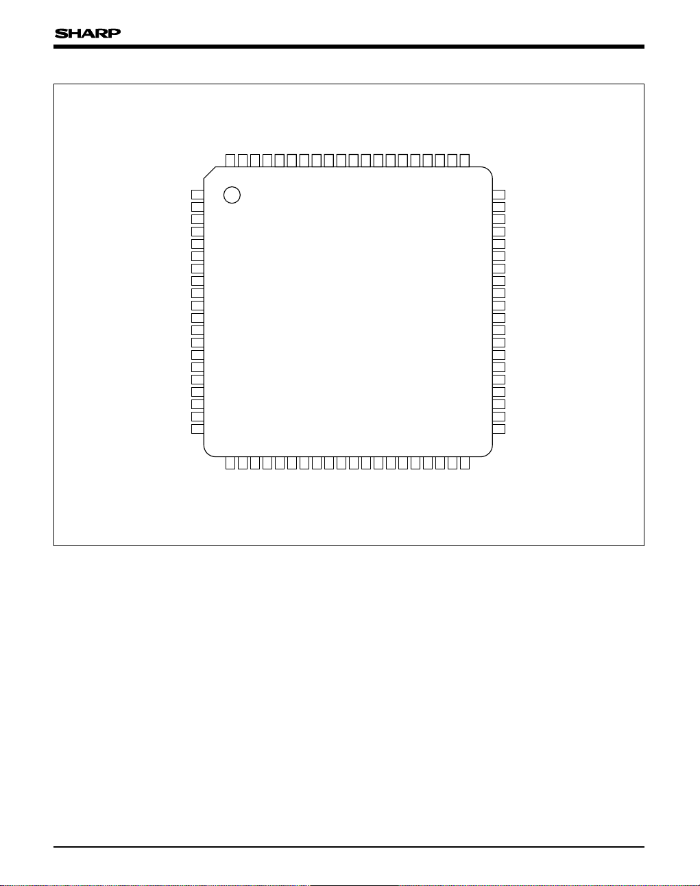
PIN CONNECTIONS
1
2
3
4
5
6
7
8
9
10
11
12
13
14
15
16
17
18
19
20
60
59
58
57
56
55
54
53
52
51
50
49
48
47
46
45
44
43
42
41
21222324252627282930313233343536373839
40
ACL
CKI
CKO
V
DD
GND
ADCK
SCK
SDATA
ADI
9
ADI8
ADI7
ADI6
ADI5
ADI4
VDD
GND
ADI
3
ADI2
ADI1
ADI0
OBCP
ADCLP
BLKX
EEPDA
GND
V
DD
EEPCK
EEPFL
EEPSL
WB
1
WB2
MIR
BLC
GNDDA
V
DDDA
VB
I
REF
VREF
GNDDA
VIDEO
HD
Y
7
Y6
Y5
Y4
VDD
GND
Y
3
Y2
Y1
Y0
EXCKI
DCK
2
DCK1
VDD
GND
EEMD
3
EEMD2
EEMD1
EEMDS
80797877767574737271706968676665646362
61
FCDSFSRS
GND
VDDFH2
FH1FRGND
VDDOFDX
VH3XVH1X
GND
VDDV4X
V3X
V2X
V1X
VD
LR38603
80-PIN LQFP
TOP VIEW
(P-LQFP080-1212)
2
Page 3
BLOCK DIAGRAM
ADI9-ADI0
VIDEO
CKI
FR, FH1, FH2
V1X-V4X
VH1X, VH3X
OB
CLAMPING
4 LINES
DELAY
LUMINANCE
SIGNAL
PROCESS
9-BIT DA
COLOR
SIGNAL
PROCESS
SSG
TG
BLKX, CSYNC
HD, VD, ADCLP
OBCP
FCDS, FS, RS
ADCK
CKO
Y7-Y0
DCK1, DCK2
EXCKI
EEPSL, EEPFL
EEPCK, EEPDA
EEMD
2, EEMD3
EEMDS, EEMD1
WB1, WB2, MIR, BLC
AUTOMATIC
CONTROL
EEPROM
CONTROL
LR38603
3
Page 4
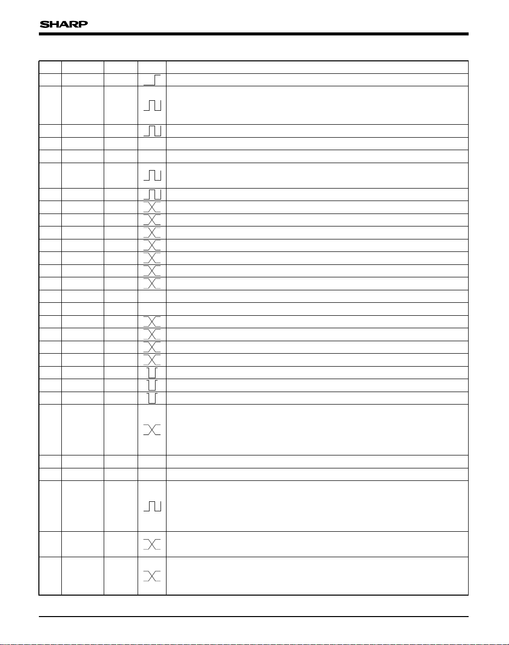
PIN DESCRIPTION
PIN NO.
SYMBOL
1 ACL ICSU All reset
2 CKI OSCI
3 CKO OSCO
DD – Power supply input (+3.3 V)
4V
5 GND – Ground
6 ADCK OBF4M
7 SCK OBF4M
8 SDATA OBF4M
9 ADI9 IC Digital signal input (MSB)
10 ADI
11 ADI
12 ADI
13 ADI
14 ADI4 IC Digital signal input
DD – Power supply input (+3.3 V)
15 V
16 GND – Ground
17 ADI
18 ADI
19 ADI1 IC Digital signal input
20 ADI
21 OBCP OBF4M
22 ADCLP OBF4M Clamp pulse output
23 BLKX OBF4M
24 EEPDA IO4MU
25 GND – Ground
DD – Power supply input (+3.3 V)
26 V
27 EEPCK IO4MSU
28 EEPFL ICU
29 EEPSL ICD
IO SYMBOL
POLARITY
Input for reference clock oscillator
Connect to CKO (pin 3) with R.
NTSC : 28.63636 MHz PAL : 28.375 MHz
Output for reference clock oscillator. The output is the inverse of CKI (pin 2).
Clock output for A/D converter
Connect to ADCK of IR3Y48A1.
Clock output for setting parameter of IR3Y48A1
Serial data output for setting parameter of IR3Y48A1
8 IC Digital signal input
7 IC Digital signal input
6 IC Digital signal input
5 IC Digital signal input
3 IC Digital signal input
2 IC Digital signal input
0 IC Digital signal input (LSB)
Clamp pulse output for optical black
Blanking pulse output
Data input from EEPROM
Connect to a data output pin of EEPROM.
When setting internal register from an external device, use EEPCK, EEPFL and
EEPSL together with EEPDA. This pin is for serial data input.
Clock output for EEPROM
Connect to clock input of EEPROM.
When setting internal register from external device, this pin is used as serial
clock.
Control for setting internal register from an external device
Usually used at H level.
Control for setting internal register from external device
Usually used at L level.
When setting register, set EEPSL at H level.
LR38603
DESCRIPTION
4
Page 5
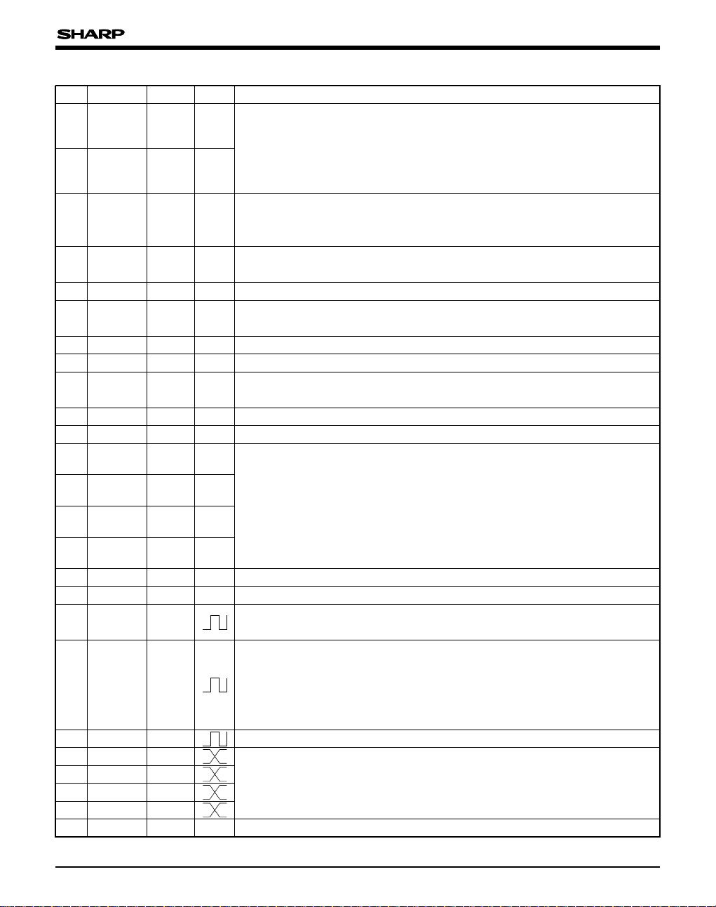
PIN NO.
SYMBOL
30 WB1 IO4MD
IO SYMBOL
POLARITY
DESCRIPTION
WB setting. Use together with WB
1 and WB2
00 (WB2, WB1) : Auto white balance 01 : WB1 mode 10 : WB2 mode
11 : WB3 mode
31 WB
2 IO4MD
These pins are 0 bit (WB
1) and 1st-bit (WB2) of UV output in output digital YUV
mode.
Setting for mirroring video output mode
32 MIR IO4MD
L : Normal H : Mirroring
This pin is 2nd-bit of UV output in output digital YUV mode.
33 BLC IO4MD
Switching internal register for exposure-standard
This pin is 3rd-bit of UV output in digital output mode.
34 GNDDA – Ground for internal D/A converter
35 V
DDDA –
Power supply for internal D/A converter
Connect to DC 3.3 V power supply (+3.3 V).
36 VB DAO DC output of internal D/A converter. Connect to ground pin via capacitor.
REF DAO DC output of internal D/A converter. Connect to ground pin via register.
37 I
REF DAI
38 V
DC reference input for internal D/A converter
Connect to DC power supply (+1.0 V).
39 GNDDA – Ground for internal D/A converter.
40 VIDEO DAO Analog video output
41 EEMDS IO4MU
42 EEMD
1 IO4MU
Switching electronic shutter control
Use together with EEMDS, EEMD
1, EEMD2 and EEMD3. Refer to "Electronic
Shutter Speed Setting" in AUTOMATIC CAMERA FUNCTION CONTROL.
These pins are 4th to 7th-bit of UV output in digital output mode.
43 EEMD
44 EEMD
2 IO4MU
3 IO4MU
When in line lock mode,
2 : H reset
EEMD
: V reset
3
EEMD
45 GND – Ground
46 V
DD – Power supply input (+3.3 V).
47 DCK
1 OBF4M
Clock output synchronized with digital output
Switchable among CSYNC, CBLK or L level.
ID pulse output of UV signal for digital output
When in analog output, output is KEI or L level.
48 DCK
2 OBF4M
KEI pulse : At power-on, begin with L level. When shutter speed is 1/60 s (PAL
1/50 s) and PGA gain is more than the value in address 92h, it goes to H level
and becomes stable.
49 EXCKI ICSU
50 Y0 OBF4M
51 Y
1 OBF4M
52 Y2 OBF4M
53 Y3 OBF4M
Input for external clock
Digital video signal output
Use together with Y
7 (MSB) to Y0 (LSB).
UYVY signal or illumination signal output (according to the register).
54 GND – Ground
LR38603
5
Page 6
PIN NO.
SYMBOL
IO SYMBOL
POLARITY
DESCRIPTION
55 VDD – Power supply input (+3.3 V)
4 OBF4M
56 Y
57 Y
5 OBF4M
6
58 Y
OBF4M
59 Y7 OBF4M
Digital video signal output
Use together with Y
7 (MSB) to Y0
(LSB).
UYVY signal or illumination signal output (according to the register)
Horizontal drive pulse output
60 HD OBF4M
It is able to select horizontal drive pulse for drive timing and video output timing
from BELL pulse, HREF pulse and L level.
BELL pulse : The signal that goes to H level 1 time per 1 field.
Vertical drive pulse output
61 VD OBF4M
It is able to select from VD, CSYNC and VS outputs for drive timing and video
output timing.
1X OBF4M
62 V
63 V2X OBF4M
64 V3X OBF4M
CCD vertical drive pulse output
Connect each pin to CCD via V driver IC.
65 V4X OBF4M
66 VDD – Power supply input (+3.3 V)
67 GND – Ground
68 VH
1X OBF4M Pulse output for reading charges
Connect each pin to CCD via V driver IC.69 VH3X OBF4M
70 OFDX OBF4M OFD pulse output. Connect each pin to CCD via V driver IC.
71 VDD – Power supply input (+3.3 V)
72 GND – Ground
73 FR
74 FH1
OBF12M
OBF12M
2
OBF12M
Reset pulse output. Connect each pin to CCD via capacitor.
Horizontal transmit pulse output
Connect to CCD.75 FH
76 VDD – Power supply input (+3.3 V)
77 GND – Ground
78 RS OBF4M
79 FS OBF4M
Pulse output for sample hold
When using IR3Y48A1, connect to CSN pin for parameter setting.
Pulse output for sample hold
80 FCDS OBF4M Pulse output for sample hold
IC : Input pin
ICU : Input pin with pull-up resistor
ICD : Input pin with pull-down resistor
ICSU : Schmidt input pin with pull-up resistor
DAI : Input pin for D/A converter
OSCI : Input pin for oscillation
OBF4M : Output pin
OBF12M : Output pin
DAO : Output pin for D/A converter
OSCO : Output pin for oscillation
IO4MU : Input/output pin with pull-up resistor
IO4MD : Input/output pin with pull-down resistor
IO4MSU : Input/output pin with pull-down resistor (schmidt
input)
LR38603
6
Page 7
DSP REGISTER TABLE
ADDRESS
00h
01h LPF_TH [7] H : Luminance signal processing without LPF (when using B/W CCD)
02h NI [6] 0 : Interlace 1 : Non-interlace
03h HD_SEL [6 : 5] Select output signal from HD pin
04h SW_CTRL [7 : 0] Electronic shutter control (EEMDS, EEMD
NAME BIT CONTENTS
STOP_EEPROM
[7 : 0] Stop reading from EEPROM only when EEPROM data is FF.
CCD_SEL [6 : 5] 00 : 270 k pixel CCD (NTSC) 01 : 410 k pixel CCD (NTSC)
10 : 320 k pixel CCD (PAL) 11 : 470 k pixel CCD (PAL)
ADTI [4 : 3] Input data timing adjustment
00 : Reference 01 : 1 clock delay 10 : 1 clock forward 11 : 2 clocks forward
[2] 1 : Latch with inverted clock
SEL_CDS [1 : 0] Fixed to 1X (IR3Y48A1)
MODE_OUT_SIG
Select output mode.
[5 : 3]
000 : Analog video output EXCKI : Vertical reset pulse input
001 : Analog video output EXCKI : 8 fsc clock input
2 : Horizontal reset pulse input EEMD
EEMD
010 : Analog video output EEMD
: Vertical reset pulse input
3
EEMD
2 : Horizontal reset pulse input
3 : Vertical reset pulse input
100 : YUV digital video output : Clock rate of video data pixel-CK
101 : YUV digital video output : Clock rate of video data EXCKI
110 : UYVY digital video output : Clock rate of video data EXCKI
011, 111 are prohibited.
START_EE [2] Shutter speed at power-on 0 : minimum 1 : maximum
AGC_FIX [1] PGA control 0 : Auto 1 : Fixed
OB_SEL [0] Carrier balance control 0 : Auto 1 : Fixed
00 : HD output (CCD drive timing) 01 : HD output (video output timing)
10 : BELL pulse (in analog video output), HREF (in digital video output)
11 : Fixed to L level
VD_SEL [4 : 3] Select output signal from VD pin
00 : VD output (CCD drive timing) 01 : VD output (video output timing)
10 : Fixed to L level (in analog video output), VS (in digital video output)
11 : Fixed to L level (in analog video output), CSYNC (in digital video
output)
DCK1_SEL [2 : 1] Select output signal from DCK
1 pin (in analog video output)
00 : CSYNC 01 : CBLNK 1X : Fixed to L level
DCK2_SEL [0] Select output signal from DCK
2 pin (in analog video output)
0 : Fluorescent signal 1 : Fixed to L level
1, EEME2, EEMD3), mirror video
output (MIR [MSB]), internal register for exposure-standard (BLC) and white
balance (WB
2, WB1 [LSB]) are set when selecting digital output mode with
MODE_OUT_SIG (address 02h).
Shutter control of EEMD
and that of EEMDS and EEMD
2 and EEMD3 is set by the register of SW_CTRL
1 is set by pin 41 and pin 42 when setting
"001" and "010" with MODE_OUT_SIG (address 02h).
LR38603
7
Page 8

LR38603
ADDRESS
05h MIN_SH_SEL [7] Select minimum shutter speed 0 : 1/60 s (1/50 s) 1 : 1/100 s (1/120 s)
06h REF_IRIS1 [7 : 0] Reference of exposure
07h CTLD_AGC [7 : 0] Outside range of error of exposure reference
08h CTLD_0 [7 : 0] Inside range of error of exposure reference
09h REF_IRIS2 [7 : 0] Exposure reference in condition against light (When BLC = H)
0Ah CLIP_IRIS [7 : 0] Ceiling clip in accumulate exposure data
0Bh UW_E1 [7 : 0] Downward weight factor 1 in calculation of exposure. (upper of screen)
0Ch UW_E2 [7 : 0] Downward weight factor 2 in calculation of exposure.
0Dh UW_E3 [7 : 0] Downward weight factor 3 in calculation of exposure.
0Eh UW_E4 [7 : 0] Downward weight factor 4 in calculation of exposure.
0Fh UW_E5 [7 : 0] Downward weight factor 5 in calculation of exposure.
10h UW_E6 [7 : 0] Downward weight factor 6 in calculation of exposure.
11h UW_E7 [7 : 0] Downward weight factor 7 in calculation of exposure.
12h UW_E8 [7 : 0] Downward weight factor 8 in calculation of exposure. (lower of screen)
13h CW_E [6 : 0] Ratio of downward IRIS against center
14h CWP_E [5 : 0] Center point, position of left-upper area.
15h CWA_E [5 : 0] Center point, size of area.
16h EE_DIV_STP [6 : 4] Select dividing value of shutter speed control.
17h P_HEE [7 : 0] Ratio of luminance H peak of IRIS data
18h P_LEE [7 : 0] Ratio of luminance L peak of IRIS data
19h MOD8 [4] Select peak accumulation. 0 : Avg. of 8 pixels 1 : Avg. of 4 pixels
1Ah AG_DIV_STP [7 : 5] Select dividing value of PGA control.
1Bh MAX_AGC [7 : 0] Upper limitation of PGA control.
1Ch REF_AGC [7 : 0] Lower limitation of PGA control (initial value of PGA at power-on).
1Dh S_38M_GA [7 : 0] Fixed PGA gain [7 : 0 (LSB) ]
1Eh S_38M_GA_U [3] Fixed PGA gain when using IR3Y48A1 [8 (MSB)]
NAME BIT CONTENTS
MAX_SH [6 : 0] Restriction in maximum shutter speed
(When EEMDS, EEMD
(Hysteresis range of IRIS and PGA tweaking range)
(Exposure control is stopped in REF_IRIS±CTLD_0)
Sum of UW_E1 to UW_E8 must be 256d.
LPFE_O [3 : 2] Select LPF of IRIS data in PGA normal adjustment.
LPFE_I [1 : 0] Select LPF of IRIS data in PGA tweak.
IRIS_DLY [3 : 2] Reduction of IRIS control in normal operation.
00 : Operating always 01 : Operating each 2VD timing
10 : Operating each 4VD timing 11 : Operating each 8VD timing
IRIS_DLY [1 : 0] Reduction of IRIS control in PGA tweak.
00 : Operating always 01 : Operating each 2VD timing
10 : Operating each 4 VD timing 11 : Operating each 8VD timing
AG_GAIN [4 : 0] Number of steps in PGA gain
S_38M_MX
IR3Y48A1 minimum gain [1 : 0]
[2 : 0]
00 : 0 01 : +6 dB 10 : +12 dB 11 : –2 dB
1, EEMD2
, EEMD3 = 4' b1110)
8
Page 9

LR38603
ADDRESS
1Fh S_38M_OFS
20h CSEPR [7 : 0] R side factor of color separation (positive value)
21h CSEPB [7 : 0] B side factor of color separation (positive value)
22h CB_R
23h CB_B [7 : 0] B side factor of carrier balance (complement of 2)
24h
25h
26h
27h
28h
29h
2Ah
2Bh K_WBR_H [7 : 0] R side multiplier of capture speed in AWB fast processing.
2Ch
2Dh
2Eh AWB_HCL [7 : 0] Initial value of AWBHCL
2Fh AWB_LCL [7 : 0] Initial value of AWBLCL
30h REF_WBPK [7 : 0] Reference data in calculation of intercept level of AWB accumulated luminance
31h K_CL [7 : 0] H peak ratio in calculation of intercept level of AWB accumulated luminance
32h K_WBCL [7 : 0] Multiplier in calculation of intercept level of AWB accumulated luminance
33h
NAME BIT CONTENTS
[7] Offset auto adjustment.
0 : Auto 1 : Fixed (when using IR3Y48A1)
[6 : 0] Factor in fixed offset mode
Fixed to 40h when using IR3Y48A1.
[7 : 0] R side factor of carrier balance (complement of 2)
C_GAM [5 : 3] Select characteristics of color gamma.
YL_SEL [2 : 1] Manner of YL signal production ([2 : 1])
00 : Avg. of 3 lines 01 : Each R, B line 1X : Fixed ratio
C1_RB_SEL [0] Manner of RG signal production
0 : Use color separation factor (address 20h, 21h)
1 : Use fixed color separation factor.
MODE_MAT [7] Matrix factor 0 : Unsigned 1 : Signed
LC_ON_RB [6] 1 : Operation against line crawl in color processing.
YL_SUB [5] 1 : Set YL to 0 in chrominance generation.
UV_CTRL1 [4] Switch order of UV digital output
SEL_RB [3] Swap R and B after color separation.
SEL_RB2 [2] Swap R – Y and B – Y in output
SPCTRL [1] Switch attributes of SP1 and SP2.
IDCO [0] Switch attribute of color separation HG.
MAX_WBR [7 : 0] Upper limit of R side range of AWB gain (9 bits data which includes 1 at LSB)
MIN_WBR [7 : 0] Lower limit of R side range of AWB gain (9 bits data which includes 1 at LSB)
MAX_WBB [7 : 0] Upper limit of B side range of AWB gain (9 bits data which includes 1 at LSB)
MIN_WBB [7 : 0] Lower limit of B side range of AWB gain (9 bits data which includes 1 at LSB)
JMP_OFF [4] 0 : Normal 1 : Suppress AWB skipping
AWB_HIGH [3] 0 : Normal 1 : Force fast processing in small frame
MAX_IQAREA [2] 0 : Address 36h to 3Dh 1 : Fix WB frame to maximum.
IQ_LPF [1 : 0] Select LPF of AWB I, Q.
00 : Avg. of 4 V 01 : Avg. of 2 V 1X : Non
K_WBB_H [7 : 0] B side multiplier of capture speed in AWB fast processing.
CMP_CT [7 : 0] Number of operations of white balance (each CMP_CT x VD timing)
INT_I_R_Y [7] AWB detected data
0 : I, Q 1 : R – Y, B – Y
CW_IQ [6 : 0] Ratio of AWB weighted center and downward.
9
Page 10

LR38603
ADDRESS
34h
NAME BIT CONTENTS
CWPA_IQ [7 : 0] Position and area of AWB center.
35h CTLD_AW0 [7 : 0] Reset range of WB frame (compared with IRIS)
36h AWB_IP_L [7 : 0] Outside, I-axis positive of AWB detect area (in fast processing)
37h AWB_IM_L [7 : 0] Outside, I-axis negative of AWB detect area (in fast processing)
38h AWB_QP_L [7 : 0] Outside, Q-axis positive of AWB detect area (in fast processing)
39h AWB_QM_L [7 : 0] Outside, Q-axis negative of AWB detect area (in fast processing)
3Ah AWB_IP_S [7 : 0] Inside, I-axis positive of AWB detect area (in normal processing)
3Bh AWB_IM_S [7 : 0] Inside, I-axis negative of AWB detect area (in normal processing)
3Ch AWB_QP_S [7 : 0] Inside, Q-axis positive of AWB detect area (in normal processing)
3Dh AWB_QM_S [7 : 0] Inside, Q-axis negative of AWB detect area (in normal processing)
3Eh
AWB_IW_L [6 : 0] White area, I-axis, outside (for hysteresis).
3Fh AWB_QW_L [6 : 0] White area, Q-axis, outside (for hysteresis).
40h AWB_IW_S [7 : 4] White area, I-axis, inside (for targeted white area).
AWB_QW_S [3 : 0] White area, Q-axis, inside (for targeted white area).
41h AWB_C_I [7 : 4] WB convergence orientation, I-axis coordinate (complement of 2)
AWB_C_Q [3 : 0] WB convergence orientation, Q-axis coordinate (complement of 2)
42h WBR1 [7 : 0] WB
43h WBB1 [7 : 0] WB
44h WBR2 [7 : 0] WB
1 R side constant (9 bits data which includes 0 at MSB)
B side constant (9 bits data which includes 0 at MSB)
1
2 R side constant (9 bits data which includes 0 at MSB)
45h WBB2 [7 : 0] WB2 B side constant (9 bits data which includes 0 at MSB)
46h WBR3 [7 : 0] WB
3 R side constant (9 bits data which includes 0 at MSB)
47h WBB3 [7 : 0] WB3 B side constant (9 bits data which includes 0 at MSB)
48h REF_GA_R1M [7 : 0] Chrominance gain of R – Y negative direction when WB
1 is fixed or auto-
controlled (present WBR factor ≤ WBR1).
49h REF_GA_B1M [7 : 0] Chrominance gain of B – Y negative direction when WB
1 is fixed or auto-
controlled (present WBR factor ≤ WBR1).
is fixed or auto-
4Ah
REF_GA_R1P [7 : 0] Chrominance gain of R – Y positive direction when WB
1
controlled (present WBR factor ≤ WBR1).
4Bh REF_GA_B1P [7 : 0] Chrominance gain of B – Y positive direction when WB
1 is fixed or auto-
controlled (present WBR factor ≤ WBR1).
4Ch
REF_GA_R2M [7 : 0] Chrominance gain of R – Y negative direction when WB
2 is fixed or auto-
controlled (present WBR factor ≤ WBR2).
4Dh REF_GA_B2M [7 : 0] Chrominance gain of B – Y negative direction when WB
2 is fixed or auto-
controlled (present WBR factor ≤ WBR2).
4Eh REF_GA_R2P [7 : 0] Chrominance gain of R – Y positive direction when WB
2 is fixed or auto-
controlled (present WBR factor ≤ WBR2).
4Fh REF_GA_B2P [7 : 0] Chrominance gain of B – Y positive direction when WB
2 is fixed or auto-
controlled (present WBR factor ≤ WBR2).
50h REF_GA_R3M [7 : 0] Chrominance gain of R – Y negative direction when WB
3 is fixed or auto-
controlled (present WBR factor ≤ WBR3).
51h REF_GA_B3M [7 : 0] Chrominance gain of B – Y negative direction when WB
3 is fixed or auto-
controlled (present WBR factor ≤ WBR3).
10
Page 11

LR38603
ADDRESS
NAME BIT CONTENTS
52h REF_GA_R3P [7 : 0] Chrominance gain of R – Y positive direction when WB3 is fixed or auto-
controlled (present WBR factor ≤ WBR3).
53h REF_GA_B3P [7 : 0] Chrominance gain of B – Y positive direction when WB
3 is fixed or auto-
controlled (present WBR factor ≤ WBR3).
54h K_GA_R1M [6 : 0] Chrominance gain slope of R – Y negative direction in WB auto control
(WBR1 < present WBR < WBR2)
55h K_GA_B1M [6 : 0] Chrominance gain slope of B – Y negative direction in WB auto control
(WBR1 < present WBR < WBR2)
56h K_GA_R1P [6 : 0] Chrominance gain slope of R – Y positive direction in WB auto control
(WBR1 < present WBR < WBR2)
57h K_GA_B1P [6 : 0] Chrominance gain slope of B – Y positive direction in WB auto control
(WBR1 < present WBR < WBR2)
58h K_GA_R2M [6 : 0] Chrominance gain slope of R – Y negative direction in WB auto control
(WBR2 < present WBR < WBR3)
59h K_GA_B2M [6 : 0] Chrominance gain slope of B – Y negative direction in WB auto control
(WBR2 < present WBR < WBR3)
5Ah K_GA_R2P [6 : 0] Chrominance gain slope of R – Y positive direction in WB auto control
(WBR2 < present WBR < WBR3)
5Bh K_GA_B2P [6 : 0] Chrominance gain slope of B – Y positive direction in WB auto control
(WBR2 < present WBR < WBR3)
5Ch REF_MAT_R1M [5 : 0] Matrix correction factor of R – Y negative direction when WB
1 is fixed or
autocontrolled (present WBR factor ≤ WBR1).
5Dh REF_MAT_B1M [5 : 0] Matrix correction factor of B – Y negative direction when WB
1 is fixed or
autocontrolled (present WBR factor ≤ WBR1).
5Eh REF_MAT_R1P [5 : 0] Matrix correction factor of R – Y positive direction when WB
1 is fixed or
autocontrolled (present WBR factor ≤ WBR1).
is fixed or
5Fh REF_MAT_B1P [5 : 0] Matrix correction factor of B – Y positive direction when WB
1
autocontrolled (present WBR factor ≤ WBR1).
60h REF_MAT_R2M [5 : 0] Matrix correction factor of R – Y negative direction when WB
2 is fixed or
autocontrolled (present WBR factor = WBR2).
61h REF_MAT_B2M [5 : 0] Matrix correction factor of B – Y negative direction when WB
2 is fixed or
autocontrolled (present WBR factor = WBR2).
62h REF_MAT_R2P [5 : 0] Matrix correction factor of R – Y positive direction when WB
2 is fixed or
autocontrolled (present WBR factor = WBR2).
63h REF_MAT_B2P [5 : 0] Matrix correction factor of B – Y positive direction when WB
2 is fixed or
autocontrolled (present WBR factor = WBR2).
64h REF_MAT_R3M [5 : 0] Matrix correction factor of R – Y negative direction when WB
3 is fixed or
autocontrolled (present WBR factor = WBR3).
65h REF_MAT_B3M [5 : 0] Matrix correction factor of B – Y negative direction when WB
3 is fixed or
autocontrolled (present WBR factor = WBR3).
66h REF_MAT_R3P [5 : 0] Matrix correction factor of R – Y positive direction when WB
3 is fixed or
autocontrolled (present WBR factor = WBR3).
11
Page 12

LR38603
ADDRESS
67h REF_MAT_B3P [5 : 0] Matrix correction factor of B – Y positive direction when WB3 is fixed or
68h K_MAT_R1M [7 : 0] Matrix correction slope factor of R – Y negative direction in WB auto control
69h K_MAT_B1M [7 : 0] Matrix correction slope factor of B – Y negative direction in WB auto control
6Ah K_MAT_R1P [7 : 0] Matrix correction slope factor of R – Y positive direction in WB auto control
6Bh K_MAT_B1P [7 : 0] Matrix correction slope factor of B – Y positive direction in WB auto control
6Ch K_MAT_R2M [7 : 0] Matrix correction slope factor of R – Y negative direction in WB auto control
6Dh K_MAT_B2M [7 : 0] Matrix correction slope factor of B – Y negative direction in WB auto control
6Eh K_MAT_R2P [7 : 0] Matrix correction slope factor of R – Y positive direction in WB auto control
6Fh K_MAT_B2P [7 : 0] Matrix correction slope factor of B – Y positive direction in WB auto control
70h
71h COL_S [7 : 0] Start point of low luminance color suppression (PGA gain).
72h COL_H [5 : 0] Low luminance color suppression gain.
73h CKI_HCL [7 : 0] Start level of high luminance color suppression.
74h CKI_LCL [7 : 0] Start level of low luminance color suppression.
75h CKI_HLGA
76h
77h CKI_HECL [7 : 0] Start point of horizontal edge color suppression.
78h CKI_EVCL [7 : 0] Start point of vertical edge color suppression.
79h CKI_EGA
7Ah
7Bh
7Ch
NAME BIT CONTENTS
autocontrolled (present WBR factor = WBR3).
(WBR1 < present WBR < WBR2)
(WBR1 < present WBR < WBR2)
(WBR1 < present WBR < WBR2)
(WBR1 < present WBR < WBR2)
(WBR2 < present WBR < WBR3)
(WBR2 < present WBR < WBR3)
(WBR2 < present WBR < WBR3)
(WBR2 < present WBR < WBR3)
CKIL_OFF [6] 1 : Color killer OFF
COL_Y [5 : 0] Start point of luminance color suppression in maximum PGA gain.
[7 : 4] High luminance color suppression gain.
[3 : 0] Low luminance color suppression gain.
CKI_HLTI
NSUP_R
NSUP_B [3 : 0] B – Y signal low level suppression
LC_ON_YL
Y_GAM [6 : 4] Select characteristics of luminance gamma.
SEL_LPF_Y [3] Select characteristics of luminance LPF.
Y_SEL [2] Switch luminance signal processing 0 : Use only 1H 1 : 3-line process
VAPT_OFF
HAPT_OFF [0] 1 : Horizontal aperture is OFF
HAPT_SEL [7] Switch characteristics of horizontal aperture.
APT_HTIM [6 : 5] Timing of horizontal aperture : –1 to +1
APT_HGA [4 : 0] Initial value of APT_HGA (gain of horizontal edge signal)
[5 : 3] Timing adjustment of high luminance color suppression : –2 to +2
[2 : 0] Timing adjustment of low luminance color suppression : –2 to +2
[7 : 4] Gain of horizontal edge color suppression.
[3 : 0] Gain of vertical edge color suppression.
[7 : 4] R – Y signal low level suppression
[7] 1 : Execute measure against line crawl in processing luminance signal.
[1] 1 : Vertical aperture is OFF
0 : (–1 + Z1) (1 – Z2) 1 : (–1 + Z1) (1 – Z1)
12
Page 13

LR38603
ADDRESS
7Dh APT_HCL [6 : 0] Suppression level of horizontal edge signal.
7Eh APT_VGA [4 : 0] Initial value of APT_VGA (gain of vertical edge signal)
7Fh APT_VCL [6 : 0] Suppression level of vertical edge signal.
80h
81h APT_H [5 : 0] Gain of edge signal suppression.
82h
83h
84h
85h LC_K1 [7 : 0] Difference of 0H, 2H signal allowed level, for judgment of line crawl.
86h LC_K2 [7 : 0] Difference of R, B signal allowed level, for judgment of line crawl.
87h
88h
89h BAS_R [7] Sign of burst level R – Y 1 : – direction 0 : + direction
8Ah BAS_B [7] Sign of burst level B – Y 1 : – direction 0 : + direction
8Bh OUTGA [6] 1 : Mute in encoder.
8Ch SYNCLEV
8Dh MUTE_OUT
8Eh SEL_FH [7] Switch attribute of FH 1 : Inverted
8Fh SEL_FH2 [7 : 6] FH
90h STANDBY
NAME BIT CONTENTS
APT_S [7 : 0] Start point of edge signal suppression (PGA gain).
APT_Y [5 : 0] Start point of edge signal suppression in maximum PGA gained luminance.
CKI_HCL2 [7 : 0] Luminance suppression point of high luminance aperture.
CKI_ETI [6] Select level of edge signal, used in internal calculation. 1 : 1/4 times
[5 : 3] Delete timing of horizontal edge : –2 to +2
[2 : 0] Delete timing of vertical edge : –2 to +2
LC_MAX [7 : 0] Judgment of luminance level, for judgment of line crawl.
SETUP [6] Switch CBLK level.
[5 : 0] Adjustment of setup level (complement of 2).
[6 : 0] Burst level R – Y.
[6 : 0] Burst level B – Y (sign + absolute value).
[5] 1 : Stop adding SYNC to analog output.
[4 : 0] Gain of analog output (1 time at 10h).
[7 : 0] Adjustment of SYNC level.
[7] 1 : Disable output mute at power-on.
[6 : 0] Period of mute (MUTE_OUT x 2 vertical period)
SEL_FR [6] Switch attribute of FR 1 : Inverted
SEL_ADCK [5 : 3] ADCK phase adjustment
When using 270 k, 320 k-pixel CCDs 000 : standard to 101 : 300˚ (delayed
from "000" to "101" every 60˚.)
When using 410 k, 470 k-pixel CCDs 000 : standard to 101 : 270˚ (delayed
from "000" to "101" every 45˚.)
SEL_FS
SEL_FCDS [5 : 3] FCDS phase adjustment 000 : standard to 111 : 14 ns delay (delayed from
SEL_RS
[2 : 0] FS phase adjustment 000 : standard to 111 : 14 ns delay (delayed from
"000" to "111" every 2 ns.)
2 phase adjustment
00 : standard 01 : 1 ns delay 10 : 2 ns delay 11 : 3 ns delay
"000" to "111" every 2 ns.)
[2 : 0] RS phase adjustment 000 : standard to 111 : 14 ns delay (delayed from
"000" to "111" every 2 ns.)
[6] 1 : Standby
[5 : 0] Period of return from standby (STANDBY x vertical period)
13
Page 14

LR38603
ADDRESS
91h KNEE [7] 1 : Invert OBCP clock
92h KEI_KEISU [7 : 0] Gain of PGA which produces KEI pulse.
93h ENCIN_PH [3] Latch encoder clock inverted.
94h ANA_VARI [6 : 4] Delay adjustment of addition of luminance and color modulation.
95h BUNSYU8_SEL [7] Output 1/8 of original clock from DCK
96h REF_AW [7 : 0] Factor for white detect correction
97h REF_BW [7 : 0] Factor for white detect correction
98h REF_CW [7 : 0] Factor for white detect correction
99h REF_DW [7 : 0] Factor for white detect correction
9Ah REF_AB [7 : 0] Factor for black detect correction
9Bh REF_BB [7 : 0] Factor for black detect correction
9Ch REF_CB [7 : 0] Factor for black detect correction
NAME BIT CONTENTS
[6] 1 : Invert DCK2INV_DCK2
INV_DCK1 [5] 1 : Invert DCK1
BUSY_SEL [4] 1 : Reset auto control factor, when EEPSL is at H.
EI_ON_SEL [3] 1 : Enable KEI pulse function.
HRI_SEL [2] 1 : Invert HRES (minus attribute)
VRI_SEL [1] 1 : Invert VRES (minus attribute)
IN_VRES [0] Select vertical reset timing.
0 : Reset at CSYNC pulse timing.
1 : Reset at VD pulse timing.
[2] 1 : Enable DFF.
VARI_ENC [1 : 0] Delay adjustment of addition of luminance and color modulation.
(Delay of color signal)
00 : 0 clock delay to 11 : 3 clocks delay (delayed from "00" to "11" every 1
clock .) 1 clock : Original clock
(Delay of luminance signal)
101 : –3 clocks delay to 011 : 3 clocks delay (delayed from "101" to "011"
every 1 clock .)
1 clock : Pixel CK (complement of 2)
VARI_Y [3 : 0] Timing adjustment of luminance processing.
1001 : –7 clocks delay to 0111 : 7 clocks delay (delayed from "1001" to
"0111" every 1 clock.) 1 clock : Pixel CK (complement of 2)
.
1
TEST [6] Test mode. Set 0 in normal operation.
(The LR38603 does not read EEPROM and registers are set by serial data.)
STDBY [5] Make D/A converter standby.
CHG_CKIL [4] Swap R and B of color killer.
CHG_WB [3] Swap R and B of white balance.
CHG_MTX [2] Swap R and B of matrix input.
CHG_CCD4 [1] Swap U and V of digital output.
HG_YL_SEL [0] Swap YL line selection for each R and B.
14
Page 15

LR38603
ADDRESS
9Dh REF_DB [7 : 0] Factor for black detect correction
9Eh AWNC_SEL [5 : 0] ON/OFF control signal for each condition.
9Fh APT_O_LIM [7 : 0] Limiter of aperture output.
A0h WN00H [7 : 0] Lower bits of horizontal coordinate 1 of white defect.
A1h WN00V [7 : 0] Lower bits of vertical coordinate 1 of white defect.
A2h WN00HV [3 : 0] [3 : 2] Upper bits of vertical coordinate 1 of white defect.
A3h WN01H [7 : 0] Lower bits of horizontal coordinate 2 of white defect.
A4h WN01V [7 : 0] Lower bits of vertical coordinate 2 of white defect.
A5h WN01HV [3 : 0] [3 : 2] Upper bits of vertical coordinate 2 of white defect.
A6h WN02H [7 : 0] Lower bits of horizontal coordinate 3 of white defect.
A7h WN02V [7 : 0] Lower bits of vertical coordinate 3 of white defect.
A8h WN02HV [3 : 0] [3 : 2] Upper bits of vertical coordinate 3 of white defect.
A9h WN03H [7 : 0] Lower bits of horizontal coordinate 4 of white defect.
AAh WN03V [7 : 0] Lower bits of vertical coordinate 4 of white defect.
ABh WN03HV [3 : 0] [3 : 2] Upper bits of vertical coordinate 4 of white defect.
ACh WN04H [7 : 0] Lower bits of horizontal coordinate 5 of white defect.
ADh WN04V [7 : 0] Lower bits of vertical coordinate 5 of white defect.
AEh WN04HV [3 : 0] [3 : 2] Upper bits of vertical coordinate 5 of white defect.
AFh WN05H [7 : 0] Lower bits of horizontal coordinate 6 of white defect.
B0h WN05V [7 : 0] Lower bits of vertical coordinate 6 of white defect.
B1h WN05HV [3 : 0] [3 : 2] Upper bits of vertical coordinate 6 of white defect.
B2h WN06H [7 : 0] Lower bits of horizontal coordinate 7 of white defect.
B3h WN06V [7 : 0] Lower bits of vertical coordinate 7 of white defect.
B4h WN06HV [3 : 0] [3 : 2] Upper bits of vertical coordinate 7 of white defect.
B5h WN07H [7 : 0] Lower bits of horizontal coordinate 8 of white defect.
B6h WN07V [7 : 0] Lower bits of vertical coordinate 8 of white defect.
B7h WN07HV [3 : 0] [3 : 2] Upper bits of vertical coordinate 8 of white defect.
C0h TST_SEL31 [7 : 0] Test address (Set 00h)
C1h TST_SEL32 [7 : 0] Test address (Set 00h)
C2h TST_SEL33 [0] Test address (Set 00h)
C3h TST_SEL1A [7 : 0] Test address (Set 00h)
C4h TST_SEL1B [7 : 0] Test address (Set 00h)
C5h TST_SEL1C [7 : 0] Test address (Set 00h)
NAME BIT CONTENTS
[1 : 0] Upper bits of horizontal coordinate 1 of white defect.
[1 : 0] Upper bits of horizontal coordinate 2 of white defect.
[1 : 0] Upper bits of horizontal coordinate 3 of white defect.
[1 : 0] Upper bits of horizontal coordinate 4 of white defect.
[1 : 0] Upper bits of horizontal coordinate 5 of white defect.
[1 : 0] Upper bits of horizontal coordinate 6 of white defect.
[1 : 0] Upper bits of horizontal coordinate 7 of white defect.
[1 : 0] Upper bits of horizontal coordinate 8 of white defect.
15
Page 16

LR38603
ADDRESS
C6h TST_SEL1D [1 : 0] Test address (Set 00h)
C7h TST_SEL1V1 [7 : 0] Test address (Set 00h)
C8h TST_SEL1V2 [7 : 0] Test address (Set 00h)
C9h TST_SEL1V3 [7 : 0] Test address (Set 00h)
CAh TST_SEL1V4 [7 : 0] Test address (Set 00h)
CBh TST_C2_OB3 [6 : 0] Test address (Set 00h)
CCh TST_C2_OB4 [6 : 0] Test address (Set 00h)
CDh TST_C2_DL1 [7 : 0] Test address (Set 00h)
CEh TST_C2_DL2 [7 : 0] Test address (Set 00h)
CFh TST_C2_YL [5 : 0] Test address (Set 00h)
D0h
D1h TST_SSG_SEL [2] Test address (Set 00h)
D2h TST_C6_00 [7 : 0] Test address (Set 00h)
D3h TST_C6_01 [7 : 0] Test address (Set 00h)
D4h TST_C6_02 [6 : 0] Test address (Set 00h)
D5h TST_C4_IO0 [7 : 0] Test address (Set 00h)
D6h TST_C4_IO1 [4 : 0] Test address (Set 00h)
D7h TST_C4_IO2 [7 : 0] Test address (Set 00h)
D8h TST_C4_S0 [7 : 0] Test address (Set 00h)
D9h TST_C4_S1 [7 : 0] Test address (Set 00h)
DAh TST_C4_S2 [0] Test address (Set 00h)
DBh TST_C5_T0 [7 : 0] Test address (Set 00h)
DCh TST_C5_T1 [7 : 0] Test address (Set 00h)
DDh TST_C5_T2 [5 : 0] Test address (Set 00h)
DEh TST_SEL71 [7 : 0] Test address (Set 00h)
DFh TST_SEL72 [1 : 0] Test address (Set 00h)
E0h TEST_C8_00 [7 : 0] Test address (Set 00h)
E1h TEST_C8_01 [7 : 0] Test address (Set 00h)
E2h TEST_C8_02 [7 : 0] Test address (Set 00h)
E3h TEST_C8_03 [7 : 0] Test address (Set 00h)
E4h TEST_C8_04 [7 : 0] Test address (Set 00h)
E5h TEST_C8_05 [7 : 0] Test address (Set 00h)
E6h TEST_C8_06 [7 : 0] Test address (Set 00h)
E7h TEST_C8_07 [7 : 0] Test address (Set 00h)
E8h TEST_C8_08 [7 : 0] Test address (Set 00h)
E9h TEST_C8_09 [6 : 0] Test address (Set 00h)
F0h TST_REG1 [7 : 0] Test address (Set 00h)
F1h TST_REG2 [7 : 0] Test address (Set 00h)
F2h TST_REG3 [7 : 0] Test address (Set 00h)
F3h TST_REG4 [7 : 0] Test address (Set 00h)
NAME BIT CONTENTS
TST_C2_GAMMA1
TST_C2_GAMMA2
[7 : 0] Test address (Set 00h)
[1 : 0] Test address (Set 00h)
16
Page 17

LR38603
ADDRESS
F4h TST_REG5 [7 : 0] Test address (Set 00h)
F5h TST_REG6 [7 : 0] Test address (Set 00h)
F6h TST_REG7 [5 : 0] Test address (Set 00h)
F7h TST_REG8 [7 : 0] Test address (Set 00h)
F8h TST_REG9 [7 : 0] Test address (Set 00h)
F9h TST_REGA [7 : 0] Test address (Set 00h)
FAh TST_REGB [7 : 0] Test address (Set 00h)
FBh TST_SEL_REG [5 : 0] Test address (Set 00h)
FCh WT_DAT30 [7 : 0] Test address (Set 00h)
FDh WT_DAT31 [6 : 0] Test address (Set 00h)
FEh TST_C5_WT3 [5 : 0] Test address (Set 00h)
NAME BIT CONTENTS
17
Page 18

LR38603
ABSOLUTE MAXIMUM RATINGS
PARAMETER SYMBOL
Supply voltage V
DD
Input voltage VI –0.3 to VDD + 0.3
Storage temperature
STG
RATING UNIT
–0.3 to +4.3
DD + 0.3VOOutput voltage
V
V
V–0.3 to V
˚C–55 to +150T
RECOMMENDED OPERATING CONDITIONS
PARAMETER SYMBOL
Input voltage V
DD
Output voltage TOPR –20
MIN. UNIT
3.0
TYP. MAX.
3.3 3.6
+25 +70
V
˚C
MHzFCKInput clock 28.6
ELECTRICAL CHARACTERISTICS 1 (VDD = 3.3 V±10%, TA = –20 to +70˚C)
PARAMETER SYMBOL CONDITIONS MIN. TYP. MAX. UNIT NOTE
Input "High" voltage VIH 0.8VDD V
Input "Low" voltage V
Input "High" voltage V
Hysteresis voltage V
Input "High" current |I
IL 0.2VDD V
IH 0.8VDD V
HIS 0.2 V
IH1|VIN = VDD 1.0 µA
Input "Low" current |IIL1|VIN = 0 V 1.0 µA
Input "High" current |I
IH2|VIN = VDD 2.0 µA
Input "Low" current |IIL2|VIN = 0 V 10 33 70 µA
Input "High" current |I
Input "Low" current |I
IH3|VIN = VDD 2.0 µA
IL3|VIN = 0 V 40 100 300 µA
Input "High" current |IIH4|VIN = VDD 10 33 70 µA
Input "Low" current |I
Output "High" voltage V
Output "Low" voltage V
|V
IL4
OH1 IOH
OL1 IOL = –4 mA 0.2VDD V
= 0 V 2.0 µA
IN
= +4 mA 0.8V
DD V
Output "High" voltage VOH3 IOH = +12 mA 0.8VDD V
Output "Low" voltage V
Output "High" voltage V
OL3 IOL = –12 mA 0.2VDD V
OH4 IOH = +2 mA 0.8VDD V
Output "Low" voltage VOL4 IOL = –3 mA 0.2VDD V
NOTES :
1. Applied to inputs/outputs (IO4MU, IO4MD) and inputs
(IC, ICU, ICD, OSCI).
2. Applied to input (ICSU), input/output (IO4MSU).
3. Applied to input (IC, OSCI).
4. Applied to inputs (ICU, ICSU), input/output (IO4MSU).
5. Applied to input/output (IO4MU).
6. Applied to input (ICD), input/output (IO4MD).
7. Applied to inputs/outputs (IO4MU, IO4MD), output
(OBF4M).
8. Applied to output (OBF12M).
9. Applied to output (OSCO).
1
2Input "Low" voltage VIL 0.2VDD V
3
4
5
6
7
8
9
18
Page 19

LR38603
ELECTRICAL CHARACTERISTICS 2 (VDD = 3.3±10%, TA = –20 to +70˚C)
PARAMETER SYMBOL CONDITIONS MIN. TYP. MAX. UNIT NOTE
Resolution RES 9 Bit
Error of linearity EL V
Error of differential linearity ED ±1.0 LSB
Full scaled current IFS 13 mA
REF = 1.0 V
RREF = 4.8 k$
OUT = 75 $
R
Output impedance ROUT 75 $
Reference voltage V
REF 1.0 V 2
Reference resistance RREF 4.8 k$ 3
NOTES :
1. Applied to pin (VIDEO).
2. Applied to pin (V
3. Applied to pin (I
REF).
REF).
±5.0 LSB
1
19
Page 20

LR38603
AUTOMATIC CAMERA FUNCTION CONTROL
speed is held. And then PGA gain is controlled so
that the exposure control data will be less than the
data of CTLD_0 (Address 08h).
Automatic Electronic Exposure Control
Electronic shutter speed is controlled so that the
exposure control data approach the data of
If the exposure control data are greater than the
data of CTLD_AGC (address 07h), exposure
control starts again.
REF_IRIS1 (address 06h).
Under BLC mode, the data of REF_IRIS2 (address
09h) are available instead of REF_IRIS1.
If the exposure control data are less than the data
Electronic Shutter Speed Setting
Electronic shutter speeds below can be selected by
either hardware or coefficient data.
of CTLD_AGC (address 07h), an electronic shutter
EEMDS EEMD1 EEMD2 EEMD3
00001/60 s 1/50 s
00011/100 s 1/120 s
00101/250 s 1/250 s
00111/500 s 1/500 s
01001/1 000 s 1/1 000 s
01011/2 000 s 1/2 000 s
01101/5 000 s 1/5 000 s
01111/10 000 s 1/10 000 s
10001/20 000 s 1/20 000 s
10011/50 000 s 1/50 000 s
10101/100 000 s 1/100 000 s
10111/30 s 1/25 s
11001/15 s 1/12.5 s
11011/7.5 s 1/6.25 s
1110
1111
AUTO
1/60 s to MAX_SH (address 05h)
AUTO
1/60 s to 1/100 000 s
ELECTRONIC SHUTTER SPEED
NTSC PAL
AUTO
1/50 s to MAX_SH (address 05h)
AUTO
1/50 s to 1/100 000 s
A slower shutter speed of less than 1/60 s (1/50 s
of PAL) can make images whose interval is every
two fields, every four fields, etc.
VD pulse is also converted to the same frequency
as the output image rate.
Electronic exposure control data come from the
following equation using averaged luminance levels
of 64 areas in one image, made by DSP.
20
Page 21

LR38603
Electronic exposure control data =
[{Weighted data 1
q x (64 – CW_E (address 13h))
+ Weighted data 2 w x CW_E}/64
x (256 – P_HEE (address 17h) – P_LEE (address 18h))
+ Top level e x P_HEE + Bottom level r x
P_LEE]/256
Y11 Y12 Y13 Y14 Y15 Y16 Y17 Y18
Y21 Y22 Y23 Y24 Y25 Y26 Y27 Y28
Y31 Y32 Y33 Y34 Y35 Y36 Y37 Y38
Y41 Y42 Y43 Y44 Y45 Y46 Y47 Y48
Y51 Y52 Y53 Y54 Y55 Y56 Y57 Y58
Y61 Y62 Y63 Y64 Y65 Y66 Y67 Y68
Y71 Y72 Y73 Y74 Y75 Y76 Y77 Y78
Y81 Y82 Y83 Y84 Y85 Y86 Y87 Y88
q Weighted data 1
This comes from the following equation weighting in
horizontal.
Weighting factors are the data from UW_E1
(address 0Bh) to UW_E8 (address 12h).
Weighted data 1 =
11 + Y12 + π + Y18)/8 x UW_E1 (address 0Bh)
{(Y
+ (Y
+ Y22 + π + Y28)/8 x UW_E2 (address 0Ch)
21
:
81 + Y82 + π + Y88)/8 x UW_E8 (address
+ (Y
12h)}/256
e Top level : The highest luminance data in one
image by averaging either 4 pixels
or 8 pixels in horizontal.
r Bottom level : The lowest luminance data in
one image by averaging either 4
pixels or 8 pixels in horizontal.
Auto White Balance Control
If white balance control data are less than the data
of AWB_IW_S and AWB_QW_S (address 40h),
then AWB stops.
If white balance control data are less than the data
of AWB_IW_L (address 3Eh) and AWB_QW_L
(address 3Fh) AWB is made active so that white
balance control data are less than the data of
AWB_IW_S and AWB_QW_S.
When the data are greater than AWB_IW_L and
AWB_QW_L, AWB will be active again.
White balance data come from the following
equation using averaged I and Q data of 16 areas
in one image.
I11 I12 I13 I14
I21 I22 I23 I24
I31 I32 I33 I34
I41 I42 I43 I44
The sum from UW_E1 to UW_E8 shall be 256.
w Weighted data 2
Weighting area can be set by the data of CWP_E
(address 14h), CWA_E (address 15h).
Weighting position can be set by the data of
CWP_E.
Weighting area size can be set by the data of
CWA_E.
Weighted data come from averaged data in chosen
area.
Q11 Q12 Q13 Q14
Q21 Q22 Q23 Q24
Q31 Q32 Q33 Q34
Q41 Q42 Q43 Q44
White balance data =
{Weighted data 3 q x (64 – CW_IQ (address 33h))
+ weighted data 4 w x CW_IQ}/64
21
Page 22

LR38603
q Weighted data 3
I (or Q) data come from the following equation.
Weighted data 3 =
11 + I12 + I13 + I
{(I
31 + I32 + I33 + I34)/4 + (I41 + I42 + I43 +
+ (I
44)/4}/4
I
w Weighted data 4
Weighting area can be chosen by CWPA_IQ
(address 34h).
Weighted data come from averaged data in chosen
area.
e White balance area setting
The sum of I and Q can be regulated by the
luminance level and the color level.
Setting available luminance level range :
High level :
AWB_HCL (address 2Eh) + [{K_CL (address 31h)
x H peak level + (256 – K_CL) x Exposure control
data}/256 – REF_WBPK (address 30h)] x
K_WBCL (address 32h)
Low level :
AWB_LCL (address 2Fh) + [{K_CL (address 31h) x
H peak level + (256 – K_CL) x Exposure control
data}/256 – REF_WBPK (address 30h)] x
K_WBCL (address 32h)
Setting target zone :
AWB_IP_L (address 36h), AWB_IM_L (address 37h)
AWB_QP_L (address 38h), AWB_QM_L (address 39h)
If white balance data are less than the data of
AWB_IW_S and AWB_QW_S (address 40h) the
target zone of auto white balance changes to the
zone by the data below.
14)/4 + (I21
+ I22 + I23 + I24)/4 +
Setting target zone :
AWB_IP_S (address 3Ah), AWB_IM_S (address 3Bh)
AWB_QP_S (address 3Ch), AWB_QM_S (address 3Dh)
Auto Color Matrix and Level
Compensation
Color matrix compensation can be done by
R – Y = R – Y±(Data1 x B – Y)
B – Y = B – Y±(Data2 x R – Y)
Color level compensation can be done by
R – Y = R – Y x Data3
B – Y = B – Y x Data4
The above data come from the following equation
along the variation of color temperature.
MODE1 : Present WBR factor < WBR1
MODE2 : WBR1 ≤ present WBR factor < WBR2
MODE3 : WBR2 ≤ present WBR factor < WBR3
MODE4 : WBR3 ≤ present WBR factor
MODE1 and MODE_MAT (address 25h) = 0
Data1 = REF_MAT_R1M (address 5Ch)
Data2 = REF_MAT_B1M (address 5Dh)
Data3 = REF_GA_R1M (address 48h)
Data4 = REF_GA_B1M (address 49h)
MODE1 and MODE_MAT = 1
Data1 = REF_MAT_R1M (address 5Ch) : B – Y < 0
REF_MAT_R1P (address 5Eh) : B – Y ≥ 0
Data2 = REF_MAT_B1M (address 5Dh) : R – Y < 0
REF_MAT_B1P (address 5Fh) : R – Y ≥ 0
Data3 = REF_GA_R1M (address 48h) : R – Y < 0
REF_GA_R1P (address 4Ah) : R – Y ≥ 0
Data4 = REF_GA_B1M (address 49h) : B – Y < 0
REF_GA_B1P (address 4Bh) : B – Y ≥ 0
22
Page 23

LR38603
MODE2 and MODE_MAT = 0
Data1 = REF_MAT_R1M + K_MAT_R1M (address
68h) x (WBR – WBR1)/32
Data2 = REF_MAT_B1M + K_MAT_B1M (address
69h) x (WBR – WBR1)/32
Data3 = REF_GA_R1M + K_GA_R1M (address
54h) x (WBR – WBR1)/32
Data4 = REF_GA_B1M + K_GA_B1M (address
55h) x (WBR – WBR1)/32
MODE2 and MODE_MAT = 1
Data1 = REF_MAT_R1M + K_MAT_R1M (address
68h) x (WBR – WBR1)/32 : B – Y < 0
REF_MAT_R1P + K_MAT_R1P (address
6Ah) x (WBR – WBR1)/32 : B – Y ≥ 0
Data2 = REF_MAT_B1M + K_MAT_B1M (address
69h) x (WBR – WBR1)/32 : R – Y < 0
REF_MAT_B1P + K_MAT_B1P (address
6Bh) x (WBR – WBR1)/32 : R – Y ≥ 0
Data3 = REF_GA_R1M + K_GA_R1M (address
54h) x (WBR – WBR1)/32 : R – Y < 0
REF_GA_R1P + K_GA_R1P (address
56h) x (WBR – WBR1)/32 : R – Y ≥ 0
Data4 = REF_GA_B1M + K_GA_B1M (address
55h) x (WBR – WBR1)/32 : B – Y < 0
REF_GA_B1P + K_GA_B1P (address
57h) x (WBR – WBR1)/32 : B – Y ≥ 0
MODE3 and MODE_MAT = 0
Data1 = REF_MAT_R2M (address 60h) +
K_MAT_R2M (address 6Ch) x (WBR –
WBR1)/32
Data2 = REF_MAT_B2M (address 61h) +
K_MAT_B2M (address 6Dh) x (WBR –
WBR1)/32
Data3 = REF_GA_R2M (address 4Ch) +
K_GA_R2M (address 58h) x (WBR –
WBR1)/32
Data4 = REF_GA_B2M (address 4Dh) +
K_GA_B2M (address 59h) x (WBR –
WBR1)/32
MODE3 and MODE_MAT = 1
Data1 = REF_MAT_R2M (address 60h) +
K_MAT_R2M (address 6Ch) x (WBR –
WBR1)/32 : B – Y < 0
REF_MAT_R2P (address 62h) +
K_MAT_R2P (address 6Eh) x (WBR –
WBR1)/32 : B – Y ≥ 0
Data2 = REF_MAT_B2M (address 61h) +
K_MAT_B2M (address 6Dh) x (WBR –
WBR1)/32 : R – Y < 0
REF_MAT_B2P (address 63h) +
K_MAT_B2P (address 6Fh) x (WBR –
WBR1)/32 : R – Y ≥ 0
Data3 = REF_GA_R2M (address 4Ch) +
K_GA_R2M (address 58h) x (WBR –
WBR1)/32 : R – Y < 0
REF_GA_R2P (address 4Eh) +
K_GA_R2P (address 5Ah) x (WBR –
WBR1)/32 : R – Y ≥ 0
Data4 = REF_GA_B2M (address 4Dh) +
K_GA_B2M (address 59h) x (WBR –
WBR1)/32 : B – Y < 0
REF_GA_B2P (address 4Fh) +
K_GA_B2P (address 5Bh) x (WBR –
WBR1)/32 : B – Y ≥ 0
MODE4 and MODE_MAT = 0
Data1 = REF_MAT_R3M (address 64h)
Data2 = REF_MAT_B3M (address 65h)
Data3 = REF_GA_R3M (address 50h)
Data4 = REF_GA_B3M (address 51h)
MODE4 and MODE_MAT = 1
Data1 = REF_MAT_R3M (address 64h) : B – Y < 0
REF_MAT_R3P (address 66h) : B – Y ≥ 0
Data2 = REF_MAT_B3M (address 65h) : R – Y < 0
REF_MAT_B3P (address 67h) : R – Y ≥ 0
Data3 = REF_GA_R3M (address 50h) : R – Y < 0
REF_GA_R3P (address 52h) : R – Y ≥ 0
Data4 = REF_GA_B3M (address 51h) : B – Y < 0
REF_GA_B3P (address 53h) : B – Y ≥ 0
23
Page 24

Color Level Suppression Under Lower
Illumination
Working PGA gain can control both R – Y level
and B – Y level by the following equation.
R – Y (B – Y) level
= {32 – (working PGA gain – COL_S (address 71h))
x COL_H (address 72h)}/32
When (working PGA gain – COL_S (address 71h))
≤ 0, ( ) = 0.
Aperture Level Suppression Under
Lower Illumination
Working PGA gain can control both the horizontal
aperture level and the vertical aperture level by the
following equation.
Horizontal aperture level
= APT_HGA (address 7Ch) x {32 – (working PGA
gain – APT_S (address 80h)) x APT_H (address
81h)}/32
Vertical aperture level
= APT_VGA (address 7Eh) x {32 – (working PGA
gain – APT_S (address 80h)) x APT_H (address
81h)}/32
LR38603
When (working PGA gain – APT_S (address 80h))
≤ 0 , ( ) = 0.
24
Page 25

Gamma Characteristic Option
256
224
192
160
128
96
64
32
0
0 64 128 192 256 320 384 448 512 576 640 704 768 832 896 960 1 024
Output Level
Input Level
111
110
101
100
011
010
001
000
256
224
192
160
128
96
64
32
0
0 64 128 192 256 320 384 448 512 576 640 704 768 832 896 960 1 024
Output Level
Input Level
111
110
101
100
011
010
001
000
• Luminance signal gamma option
Y_GAM (address 7Bh) can choose one output of
below 8 responses.
LR38603
• Color signal gamma option
C_GAM (address 24h) can choose one output from
8 responses below.
25
Page 26

1
0.1
±0.1
60
P-0.5
TYP.
80-0.2
±0.08
41
40
(1.0)
12.0
±0.2
21
(1.0)
20
(1.0)(1.0)
12.0
±0.2
14.0
±0.3
61
80
M0.08
0.10
0.125
±0.05
0.64 0.64
0.125
1.4
±0.2
14.0
±0.3
1.70
MAX.
See Detail A
0-10˚
0.64
0.55
±0.15
1.0
±0.15
1.4
±0.2
1.7
MAX
Seating plane
Package
base plane
Detail A
0.1
±0.1
0.25
PACKAGE OUTLINES
LR38603
80 LQFP (P-LQFP080-1212)
(Unit : mm)
26
 Loading...