

Page 1
DESCRIPTION
The LR38580 is a CMOS single-chip driver IC which
generates timing pulses for driving 270 k/320 kpixel B/W CCD area sensors with a dual-powersupply operation, synchronous pulses for TV
signals and processing pulses for video signals.
FEATURES
• Designed for 270 k/320 k-pixel B/W CCD area
sensors with a dual-power-supply operation
• Switchable between EIA and CCIR modes
• Electronic shutter and EE control are possible
• Maximum shutter speed is selectable from
approx. 1/100 000 s, 1/56 000 s and 1/32 000 s
• Starting shutter speed is selectable from approx.
1/100 000 s and 1/1 000 s
• Flicker-less function
• Switchable between normal and mirror images
• External synchronization is possible
• Level shifter for readout and shutter pulses included
• Dual +5 V and +12.5 V power supplies
• Package :
48-pin QFP (QFP048-P-0707) 0.5 mm pin-pitch
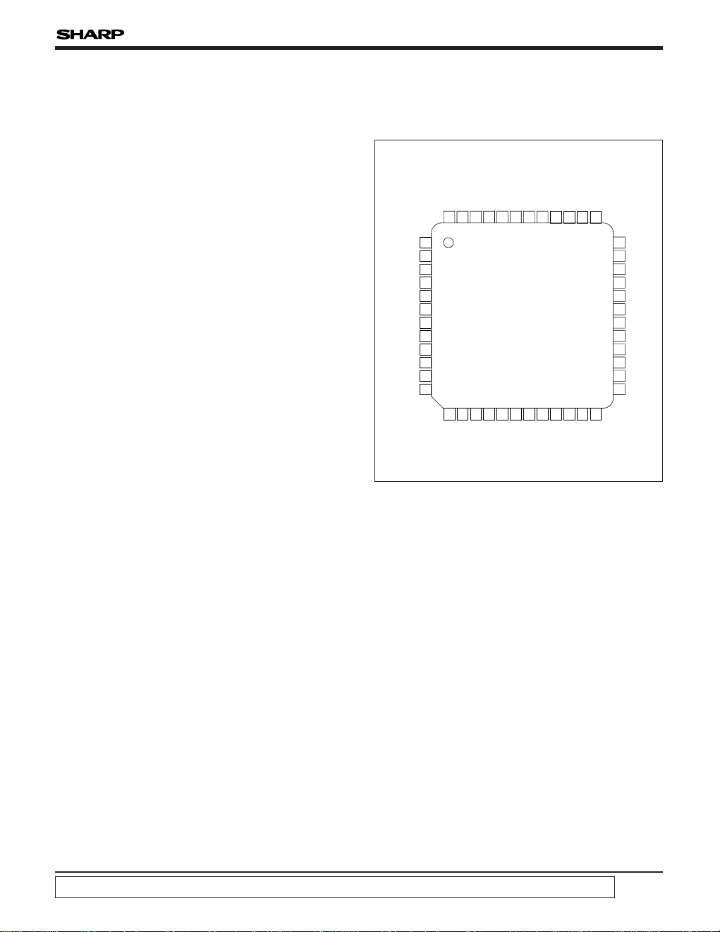
PIN CONNECTIONS
LR38580
In the absence of confirmation by device specification sheets, SHARP takes no responsibility for any defects that may occur in equipment using any SHARP devices shown in
catalogs, data books, etc. Contact SHARP in order to obtain the latest device specification sheets before using any SHARP device.
1
LR38580
Single-chip Driver IC for 270 k/320 k-pixel
B/W CCDs with Dual-power-supply Operation
1
48 47 46 45 44 43 42 41 40 39 38 37
13 14 15 16 17 18 19 20 21 22 23 24
2
3
4
5
6
7
8
9
10
11
12
36
35
34
33
32
31
30
29
28
27
26
25
TST
1
EEST
WIND
VRI
TST
2
TST3
GND
V
DD
CSYN
CBLK
OBCP
HBLK
EENR
EEUD
EEMD
VD
HD
GND
V
DD
ACLX
TVMD
TST
5
OSCO
OSCI
FLMD
MIR
V
DD
V1V2V3
V4
TST4
GND
VTG
V
DD12
OFD
GND
TST
6
FH1B
FH1
VDD
FH2
FH2BFRSTSL
FCDSFSSMAX
48-PIN QFP
TOP VIEW
(QFP048-P-0707)
Page 2
LR38580
2
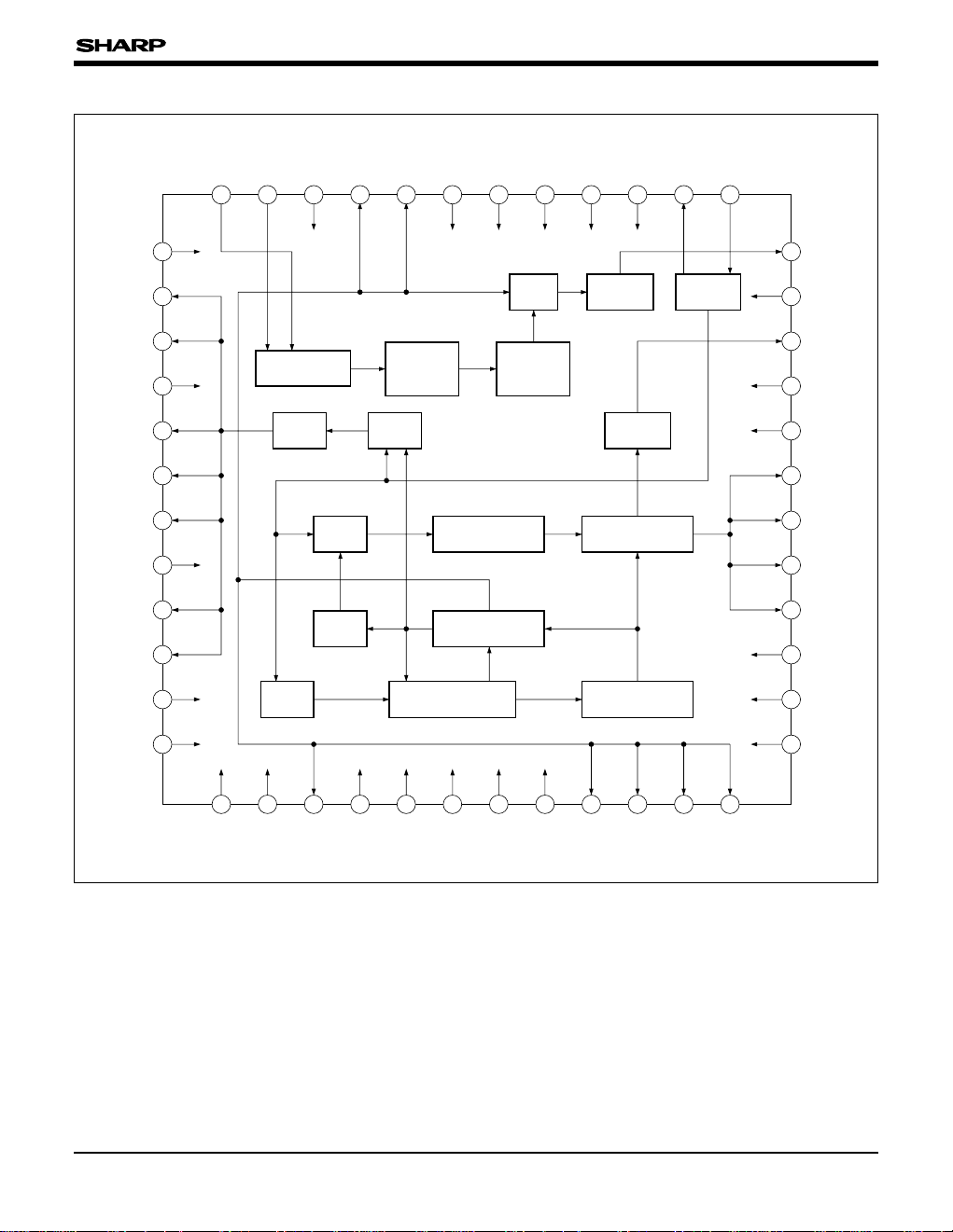
BLOCK DIAGRAM
EENR
EEUD
EEMD
VD
HD
GND
V
DD
ACLX
TVMD
TST5
OSCO
OSCI
TST
1
EEST
WIND
VRI
TST
2
TST3
GND
V
DD
CSYN
CBLK
OBCP
HBLK
OFD
V
DD12
VTG
GND
TST
4
VDD
MIR
FLMD
SMAX
FCDS
STSL
FH
2B
FH1B
TST6
GND
H/L JUDGE
SHUTTER
UP/DOWN
CONTROL
SHUTTER
SPEED
CONTROL
MIX
MIX
1/2
1/4
RESET
DECODER
DECODER
H COUNTER 2
V COUNTERH COUNTER 1
OSC
LEVEL
SHIFTER
LEVEL
SHIFTER
V
4
V3
V2
V1
FS
FR
FH
2
VDD
FH1
123456789101112
24
23
22
21
20
19
18
17
16
15
14
13
36
37
38
39
40
41
42
43
44
45
46
47
48
35 34 33 32 31 30 29 28 27 26 25
1/2
Page 3
LR38580
3
PIN DESCRIPTION
PIN NO.
SYMBOL I/O
POLARITY
PIN NAME DESCRIPTION
1 TST
1 ICD – Test pin 1 A test pin. Set open or to L level in the normal mode.
2 EEST ICU –
Electronic exposure
control input 1
An input pin to control electronic exposure using EEUD
(pin 35) and EENR (pin 36).
L level : Electronic exposure is stopped.
H level or open : Electronic exposure is operated.
3 WIND
ON
N-ch
Open
Drain
Window pulse output
An output pin for window pulse.
WIND1 : When connected to EEST (pin 2), the
operation of electronic exposure can be
stopped at the upper side of monitor.
WIND2 : A pulse that picks out the center of CCD output.
At this time, set H level or open at EEST (pin 2).
As the output circuit of WIND is N-ch open
drain, connect to V
DD with R (≥ 47 k$).
4 VRI ICSU – Vertical reset input
An input pin for resetting internal vertical counter.
The input pulse is VSYNC (negative polarity).
5 TST
2 ICD – Test pin 2 A test pin. Set open or to L level in the normal mode.
6 TST3 ICD – Test pin 3 A test pin. Set open or to L level in the normal mode.
7 GND – – Ground A grounding pin.
8V
DD – – Power supply Supply of +5 V power.
9 CSYN O
Composite
synchronizing pulse
output
An output pin of composite synchronous signal pulse.
10 CBLK O
Composite blanking
pulse output
An output pin of composite blanking pulse.
11 OBCP O
Optical black clamp
pulse output
A pulse to clamp the optical black signal. This pulse
stays low during the absence of effective pixels within
the vertical blanking.
12 HBLK O
Horizontal blanking
pulse output
A pulse that corresponds to the cease period of the
horizontal transfer pulse.
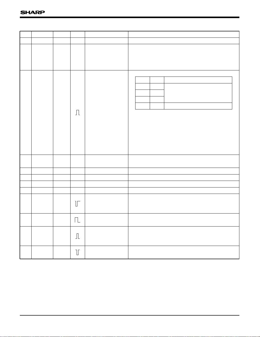
FLMD
EEMD
WIND
L
L
WIND1 (vertical pulse)H
L
L
H
H
H
WIND2 (composite pulse)
()
Page 4

LR38580
4
PIN NO.
SYMBOL I/O
POLARITY
PIN NAME DESCRIPTION
13 FLMD ICU –
Electronic exposure
and WIND pulse
control input 1
An input pin to control electronic exposure mode, flickerless mode and WIND (pin 3) pulse output.
WIND 1 : Vertical pulse
WIND 2 : Composite pulse (vertical and horizontal)
14 MIR ICU –
Mirror mode
selection input
An input pin to select mirror or normal image mode
L level : Normal image mode
H level or open : Mirror image mode
15 V
DD – – Power supply Supply of +5 V power.
16 V
1 O4MA2
Vertical transfer
pulse output 1
A pulse to drive vertical CCD shift register.
Connect to Ø
V1 pin of CCD.
17 V
2 O4MA2
Vertical transfer
pulse output 2
A pulse to drive vertical CCD shift register.
Connect to Ø
V2 pin of CCD.
18 V
3 O4MA2
Vertical transfer
pulse output 3
A pulse to drive vertical CCD shift register.
Connect to Ø
V3 pin of CCD.
19 V
4 O4MA2
Vertical transfer
pulse output 4
A pulse to drive vertical CCD shift register.
Connect to Ø
V4 pin of CCD.
20 TST4 ICD – Test pin 4 A test pin. Set open or to L level in the normal mode.
21 GND – – Ground A grounding pin.
22 VTG
O12MHV
Readout pulse
output
A pulse that transfers the charge of the photo-diode to
the vertical shift register.
Connect to VTG pin of CCD.
23 V
DD12 – – Power supply Supply of +12.5 V power.
25 OSCI OSCI – Clock input
An input pin for reference clock oscillation.
Connect to OSCO (pin 26) with R.
The frequencies are as follows :
fH = Horizontal frequency
24 OFD
O12MHV
OFD pulse output
A pulse that sweeps the charge of the photo-diode for
the electronic shutter. Connect to OFD pin of CCD.
Held at L level at normal mode.
FLMD
EEMD
Electronic Shutter mode WIND
L
L
EIA : 1/60 s, CCIR : 1/50 s
WIND1
H
L
EIA : 1/100 s, CCIR : 1/120 s
WIND1
L
H
E/E operation
WIND1
H
H
E/E operation
WIND2
MIR L (Normal mode)
H or open (Mirror mode)
FH2B ∏ FH2 ∏ FH1
∏ FH2∏ FH1FH1B
TVMD
Frequency
L 19.0699 MHz (1 212 fH)
H 19.3125 MHz (1 236 fH)
Page 5

LR38580
5
PIN NO.
SYMBOL I/O
POLARITY
PIN NAME DESCRIPTION
29 ACLX ICU – All clear input
An input pin for resetting all internal circuits at power on.
Connect V
DD through the diode and GND through the
capacitor.
30 V
DD – – Power supply Supply of +5 V power.
31 GND – – Ground A grounding pin.
32 HD O
Horizontal drive
pulse output
The pulse occurs at the start of every line.
33 VD O
Vertical drive pulse
output
The pulse occurs at the start of every field.
34 EEMD ICU –
Electronic exposure
and WIND pulse
control input 2
An input pin to control electronic exposure mode, flickerless mode and WIND (pin 3) pulse output, used with
FLMD (pin 13).
35 EEUD IC –
Electronic exposure
control input 2
An input pin to control electronic exposure.
36 EENR IC –
Electronic exposure
control input 3
37 SMAX ICU –
Shutter speed
control input 1
An input pin to control maximum and initial shutter
speed with STSL (pin 40).
38 FS O4MA2 CDS pulse output 1 A pulse to sample-hold the signal from CCD.
39 FCDS O4MA2 CDS pulse output 2 A pulse to clamp the feed-through level from CCD.
40 STSL ICU –
Shutter speed
control input 2
An input pin to control maximum and initial shutter
speed with SMAX (pin 37).
EEUD
EENR
Shutter Speed
H
L
up
H
H
control stopped
L
H
down
SMAX STSL Maximum speed Initial Speed
H H ∏ 1/ 32 000 ∏ 1/ 1 000
L H ∏ 1/ 56 000 ∏ 1/ 1 000
L L ∏ 1/101 000 ∏ 1/101 000
H L ∏ 1/101 000 ∏ 1/ 1 000
SMAX STSL Maximum Speed Initial Speed
H H ∏ 1/ 32 000 ∏ 1/ 1 000
L H ∏ 1/ 56 000 ∏ 1/ 1 000
L L ∏ 1/101 000 ∏ 1/101 000
H L ∏ 1/101 000 ∏ 1/ 1 000
28 TVMD ICU –
TV mode selection
input
An input pin to select TV standards.
L level : EIA mode
H level or open : CCIR mode
27 TST
5 ICD – Test pin 5 A test pin. Set open or to L level in the normal mode.
26 OSCO OSC3M – Clock output
An output pin for reference clock oscillation.
The output is the inverse of OSCI (pin 25).
Page 6

LR38580
6
PIN NO.
SYMBOL I/O
POLARITY
PIN NAME DESCRIPTION
41 FR O4MA3 Reset pulse output
A pulse to reset the charge of output circuit.
Connect to Ø
R pin of CCD through the DC offset circuit.
42 FH
2B O4MA2
Horizontal transfer
pulse output 2B
A pulse to drive horizontal CCD shift register.
Connect to Ø
H2B pin of CCD.
43 FH
2 O4MA3
Horizontal transfer
pulse output 2
A pulse to drive horizontal CCD shift register.
Connect to Ø
H2 pin of CCD.
45 FH
1 O4MA3
Horizontal transfer
pulse output 1
A pulse to drive horizontal CCD shift register.
Connect to Ø
H1 pin of CCD.
44 V
DD – – Power supply Supply of +5 V power.
46 FH
1B O4MA2
Horizontal transfer
pulse output 1B
A pulse to drive horizontal CCD shift register.
Connect to Ø
H1B pin of CCD.
47 TST
6 ICD – Test pin 6 A test pin. Set open or to L level in the normal mode.
48 GND – – Ground A grounding pin.
IC : Input pin (CMOS level)
ICU : Input pin (CMOS level with pull-up resistor)
ICD : Input pin (CMOS level with pull-down resistor)
ICSU : Input pin (CMOS schmitt-trigger level with pull-up
resistor)
O : Output pin (V
DD = 5 V)
O4MA2 : Output pin (V
DD = 5 V)
O4MA3 : Output pin (V
DD = 5 V)
O12MHV : Output pin (V
DD12 = 12.5 V)
ON : Output pin (N-ch open drain)
OSCI : Input pin for oscillation
OSC3M : Output pin for oscillation
Page 7

LR38580
7
SUPPLEMENTARY EXPLANATION
Shutter speed changes at electronic exposure control mode.
Select maximum shutter speed and initial shutter speed.
EIA CCIR
No. Charge Time Shutter Speed No. Charge Time Shutter Speed
0 262H or 263H ∏ 1/ 60 s 0 312H or 313H ∏ 1/ 50 s
1 252H + Ω ∏ 1/ 62 s 1 302H + ß ∏ 1/ 52 s
• (by 10H step) • (by 10H step)
19 72H + Ω ∏ 1/ 220 s 24 72H + ß ∏ 1/ 220 s
• (by 4H step) • (by 4H step)
30 28H + Ω ∏ 1/ 555 s 35 28H + ß ∏ 1/ 550 s
• (by 2H step) • (by 2H step)
37 14H + Ω ∏ 1/ 1 100 s 42 14H + ß ∏ 1/ 1 090 s
• (by 1H step) • (by 1H step)
44 7H + Ω ∏ 1/ 2 140 s 49 7H + ß ∏ 1/ 2 125 s
• (by 0.5H step) • (by 0.5H step)
50 4H + Ω ∏ 1/ 3 610 s 55 4H + ß ∏ 1/ 3 590 s
• (by 0.25H step) • (by 0.25H step)
62 1H + Ω ∏ 1/ 11 570 s 67 1H + ß ∏ 1/ 11 550 s
• (by 0.125H step) • (by 0.125H step)
69 0.125H + Ω ∏ 1/ 32 450 s 74 0.125H + ß ∏ 1/ 32 690 s
70 0.280H ∏ 1/ 56 090 s 75 0.275H ∏ 1/ 56 800 s
Ω = 0.360H ß = 0.353H
71 0.155H ∏ 1/101 430 s 76 0.152H ∏ 1/102 720 s
SMAX STSL MAXIMUM SHUTTER SPEED (s) INITIAL SHUTTER SPEED (s)
Pin 37 Pin 40 Step EIA Step CCIR Step EIA Step CCIR
H H 69 ∏ 1/ 32 450 74 ∏ 1/ 32 690 37 ∏ 1/ 1 100 37 ∏ 1/ 1 090
L H 70 ∏ 1/ 56 090 75 ∏ 1/ 56 800 37 ∏ 1/ 1 100 37 ∏ 1/ 1 090
H L 71 ∏ 1/101 430 76 ∏ 1/102 720 37 ∏ 1/ 1 100 37 ∏ 1/ 1 090
L L 71 ∏ 1/101 430 76 ∏ 1/102 720 76 ∏ 1/101 430 76 ∏ 1/102 720
Page 8

LR38580
8
ABSOLUTE MAXIMUM RATINGS
ELECTRICAL CHARACTERISTICS
DC Characteristics
(VDD = 5.0±0.5 V, VDD12 = 12.5±0.5 V, TOPR = –20 to +70 ˚C)
PARAMETER SYMBOL RATING UNIT
Supply voltage
V
DD –0.3 to +6.0 V
V
DD12 –0.3 to +15.0 V
Input voltage VI –0.3 to VDD + 0.3 V
Output voltage
V
O –0.3 to VDD + 0.3 V
Operating temperature T
OPR –20 to +70 ˚C
Storage temperature TSTG –55 to +150 ˚C
Input "Low" voltage V
IL 1.5 V
1
Input "High" voltage V
IH 3.5 V
Input "Low" voltage VT+ 3.7 V
2V
T– 1.0 V
Hysteresis voltage VT+ – VT– 0.2 V
Input "Low" current |I
IL5-1|VI = 0 V 2.0 µA
3
Input "High" current |I
IH5-1|VI = VDD 2.0 µA
Input "Low" current |IIL5-2|VI = 0 V 8.0 60 µA
4
Input "High" current |I
IH5-2|VI = VDD 2.0 µA
Output "High" voltage V
OH5-1 IOH = –2 mA 4.0 V
6
Output "Low" voltage VOL5-1 IOL = 4 mA 0.4 V
Output "High" voltage V
OH5-2 IOH = –3 mA 4.0 V
7
Output "Low" voltage VOL5-2 IOL = 3 mA 0.4 V
Output "High" voltage V
OH5-3 IOH = –6 mA 4.0 V
8
Output "Low" voltage VOL5-3 IOL = 8 mA 0.4 V
Output "High" voltage V
OH5-4 IOH = –9 mA 4.0 V
9
Output "Low" voltage V
OL5-4 IOL = 12 mA 0.4 V
Output "High" voltage V
OH12 IOH = –12 mA 12.0 V
10
Output "Low" voltage V
OL12 IOL = 12 mA 0.5 V
Output "Low" voltage V
OL5-5 IOL = 4 mA 0.4 V
11
Output leakage current |I
OZ5-5| High-Z 1.0 µA
PARAMETER SYMBOL CONDITIONS MIN. TYP. MAX. UNIT NOTE
Input "High" voltage
V–0.3 to V
DD12 + 0.3VO12
µA8.0VI = VDD|IIH5-3|Input "High" current
µA2.0
60
V
I = 0 V|IIL5-3|Input "Low" current
5
NOTES :
1. Applied to inputs (IC, ICD, ICU, OSCI).
2. Applied to input (ICSU).
3. Applied to inputs (IC, OSCI).
4. Applied to inputs (ICU, ICSU).
5. Applied to input (ICD).
6. Applied to output (O).
7. Applied to output (OSC3M). (Output (OSC3M) measures
on condition that input (OSCI) level is 0 V or V
DD).
8. Applied to output (O4MA2).
9. Applied to output (O4MA3).
10. Applied to output (O12MHV).
11. Applied to output (ON).
Page 9

PACKAGES FOR CCD AND CMOS DEVICES
9
36
25
37
48
121
0.15
±0.05
0.1
±0.1
9.0
±0.3
7.0
±0.2
7.0
±0.2
(1.0)(1.0)
(1.0)
(1.0)
0.5
TYP.
0.2
±0.08
9.0
±0.3
0.65
±0.2
1.45
±0.2
24
13
Package
base plane
8.0
±0.2
0.08
0.1
M
48 QFP (QFP048-P-0707)
PACKAGE (Unit : mm)
 Loading...