

Page 1
DESCRIPTION
The LR38516 is a CMOS timing generator IC
which is designed for video-camcorders, and which
generates timing pulses for driving 350 k-pixel
progressive scan color CCD area sensors,
synchronous pulses for TV signals and processing
pulses for video signals.
FEATURES
• Designed for 350 k-pixel progressive scan color
CCD area sensors
• Frame rate : 30 frame/s
• Shutter speed can be controlled in 1H period
using a serial code
• TV mode selection, power mode selection and
the phase selection of DCLK can be also
controlled by using a serial code
• +3 V, +4.5 V and +5 V power supplies
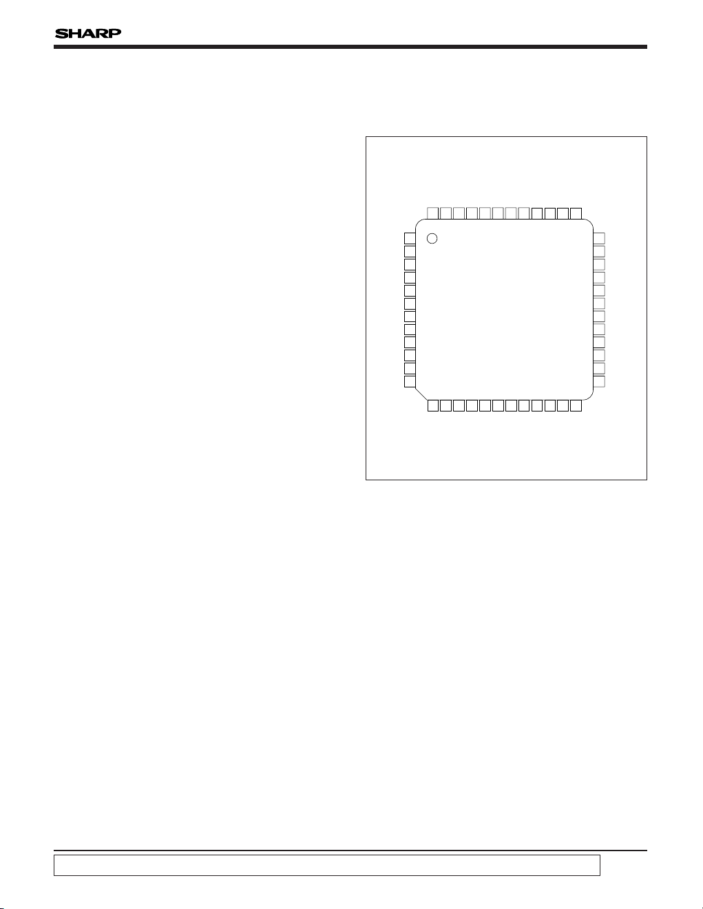
• Package :
48-pin QFP (QFP048-P-0707) 0.5 mm pin-pitch
PIN CONNECTIONS
LR38516
In the absence of confirmation by device specification sheets, SHARP takes no responsibility for any defects that may occur in equipment using any SHARP devices shown in
catalogs, data books, etc. Contact SHARP in order to obtain the latest device specification sheets before using any SHARP device.
1
LR38516
Timing Generator IC for 350 k-pixel
Progressive Scan Color CCDs
1
48 47 46 45 44 43 42 41 40 39 37
13 14 15 16 17 18 19 20 21 22 23 24
2
3
4
5
6
7
8
9
10
11
12
36
35
34
33
32
31
30
29
28
27
26
25
VTAX
VTBX
VTCX
VTDX
OFDX
V
DD3
GND
VHAX
VHCX
ID
WEN
TST
1
DBLK
GND
ADCK
NC
V
DD4
FH
2
GND
FH1V
DD4
CLRX
CCD
2
CCD
1
TST3
ED
2
ED
1
ED
0
HD
GND
V
DD3
DMVD
DCLK
CLK
CKO
CKI
PBLK
BCPX
BPX
CLPX
GND
FCDS
FS
V
DD5
RS
FR
GND
TST
2
38
48-PIN QFP
TOP VIEW
(QFP048-P-0707)
Page 2
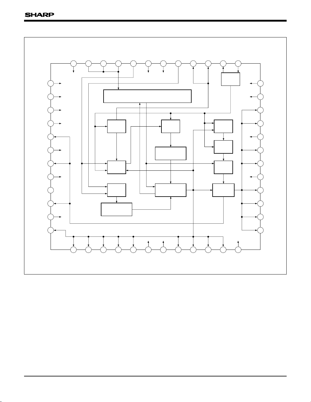
LR38516
2
BLOCK DIAGRAM
TST3
ED2
ED1
ED0
HD
GND
V
DD3
DMVD
DCLK
CLK
CKO
CKI
36 35 34 33 32 31 30 29 28 27 26 25
TST
2
GND
FR
RS
V
DD5
FS
FCDS
GND
CLPX
BPX
BCPX
PBLK
VTAX
VTBX
VTCX
VTDX
OFDX
V
DD3
GND
VHAX
VHCX
ID
WEN
TST
1
CCD1
CCD2
CLRX
V
DD4
FH1
GND
FH
2
VDD4
NC
ADCK
GND
DBLK
1/2 1/2
H COUNTER
RESET
OSC
RESET GATE
DECODER
RESET
1/2
DATA LATCH & SHUTTER CONTROL
13
14
15
16
17
18
19
20
21
22
23
24
123456789101112
48
47
46
45
44
43
42
41
40
39
38
37
LEVEL
SHIFTER
V COUNTER
Page 3
LR38516
3
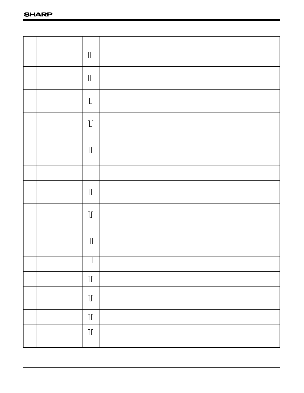
PIN NO.
SYMBOL I/O
POLARITY
PIN NAME DESCRIPTION
1 VTAX O3
Vertical transfer
pulse output 1
A vertical transfer pulse for CCD.
Connect to V
1AX pin of the vertical driver IC.
For details, see "
CONNECTION OF VERTICAL TRANSFER PULSES
".
2 VTBX O3
Vertical transfer
pulse output 2
A vertical transfer pulse for CCD.
Connect to V
2AX pin of the vertical driver IC.
For details, see "
CONNECTION OF VERTICAL TRANSFER PULSES
".
3 VTCX O3
Vertical transfer
pulse output 3
A vertical transfer pulse for CCD.
Connect to V3AX pin of the vertical driver IC.
For details, see "
CONNECTION OF VERTICAL TRANSFER PULSES
".
4 VTDX O3
Vertical transfer
pulse output 4
A vertical transfer pulse for CCD.
Connect to V4AX pin of the vertical driver IC.
For details, see "
CONNECTION OF VERTICAL TRANSFER PULSES
".
5 OFDX O3 OFD pulse output
A pulse that sweeps the charge of the photo-diode
for the electronic shutter. Connect to OFD pin of CCD
through the vertical driver IC and DC offset circuit.
Held at H level at normal mode.
6VDD3 – Power supply Supply of +3 V power.
A grounding pin.Ground–GND7–
9 VHCX O3
Readout pulse
output 3
A pulse that transfers the charge of the photo-diode to
the vertical shift register.
For details, see "
CONNECTION OF VERTICAL TRANSFER PULSES
".
8 VHAX O3
Readout pulse
output 1
A pulse that transfers the charge of the photo-diode to
the vertical shift register.
For details, see "
CONNECTION OF VERTICAL TRANSFER PULSES
".
The pulse is used in color separator. The signal
switches H and L at every line.
H : R color line
L : B color line
Line index pulse
output
O3ID 10
11 WEN O3 Write enable output Write enable output for low-speed shutter pulse.
A test pin. Set open or to L level in the normal mode.Test pin 1ICD3TST
112 –
13 PBLK O5
Pre-blanking pulse
output
A pulse that corresponds to the cease period of the
horizontal transfer pulse.
A pulse to clamp the optical black signal.
Output stays low during the absence of effective pixels
within the vertical blanking.
Optical black clamp
pulse output
O5BCPX 14
–
PIN DESCRIPTION
15 BPX O5 Clamp pulse output
A pulse to clamp the signal. The phase is same as BCPX
(pin 14). This pulse is continuous at horizontal cycle.
A pulse to clamp the dummy outputs of CCD. The pulse
stays high during the sweep-out period.
Clamp pulse outputO5CLPX16
17 GND – Ground A grounding pin.
–
Page 4

LR38516
4
PIN NO.
SYMBOL I/O
POLARITY
PIN NAME DESCRIPTION
A pulse to sample-hold the signal from CCD.
The polarity can be changed by serial data.
The output phase of FS is selected by serial data.
CDS pulse output 2O6MA5FS19
20 V
DD5 – Power supply Supply of +5 V power.
A pulse to sample-hold the signal from CDS circuit.
The polarity can be changed by serial data.
The output phase of RS is selected by serial data.
S/H pulse outputO6MA5RS21
– A grounding pin.Ground –GND 23
22 FR O6MA52 Reset pulse output
A pulse to reset the charge of output circuit.
Connect to Ø
R pin of CCD through the DC offset circuit.
The output phase of FR is selected by serial data.
24 TST
2 ICD3 Test pin 2 A test pin. Set open or to L level in the normal mode.
An input pin for reference clock oscillation.
Connect to CKO (pin 26) with R.
Frequency : 24.54545 MHz (1 560 fH)
fH = Horizontal frequency
Clock inputOSCI3CKI25 –
–26 CKO OSCO3 Clock output
An output pin for reference clock oscillation.
The output is the inverse of CKI (pin 25).
18 FCDS O6MA5 CDS pulse output 1
A pulse to clamp the feed-through level from CCD.
The polarity can be changed by serial data.
The output phase of FCDS is selected by serial data.
–
–
An output pin to generate HD and VD pulses.
Connect to clock input pin of SSG IC.
Frequency : 12.27273 MHz (780 fH)
Clock outputO6MA3CLK27
An input pin for the data of the shift register, to control
the functions of LR38516. For details, see "Serial Data
Control".
Shift register data
input
ED235 IC3 –
An output pin for DSP IC. The output phase of DCLK is
selected by serial data step by 90˚.
Frequency : 12.27273 MHz (780 fH)
Clock outputO6MA3DCLK28
An input pin for reference of vertical pulse.
Connect to VD pin of DSP IC.
Vertical reference
pulse input
IC3DMVD29
–30 V
DD3 – Power supply Supply of +3 V power.
A grounding pin.Ground –GND31 –
32 HD IC3
Horizontal reference
pulse input
An input pin for reference of horizontal pulse.
Connect to HD pin of DSP IC.
An input pin for the strobe pulse, to control the functions
of LR38516. For details, see "Serial Data Control".
Strobe pulse inputED
033 IC3 –
–IC334 ED
1
Shift register clock
input
An input pin for the clock of the shift register, to control
the functions of LR38516. For details, see "Serial Data
Control".
–ICD336 TST
3 Test pin 3 A test pin. Set open or to L level in the normal mode.
Page 5

LR38516
5
PIN NO.
SYMBOL I/O
POLARITY
PIN NAME DESCRIPTION
An input pin to select CCD.
At CCD
1 = H and CCD2 = H
1/4-type 350 k-pixel CCD (at NTSC)
At CCD
1 = H and CCD2 = L
1/3-type 350 k-pixel CCD (at NTSC)
CCD selection input 1CCD
137 ICU4 –
–ICU438 CCD
2 CCD selection input 2
–ICU439 CLRX Data clear input
An input pin for resetting all serial data at power on.
Connect VDD through the diode and GND through the
capacitor.
Supply of +4.5 V power. Power supplyV
DD440 –
O6MA4341 FH
1
Horizontal transfer
pulse output 1
A horizontal transfer pulse for CCD.
Connect to ØH1 pin of CCD.
–
–
–
A grounding pin.GroundGND42 –
O6MA4343 FH
2
Horizontal transfer
pulse output 2
A horizontal transfer pulse for CCD.
Connect to Ø
H2 pin of CCD.
Supply of +4.5 V power. Power supplyV
DD444 –
–45 NC No connection No connection.–
An output pin for A/D converter. The output phase of
ADCK is selected by serial data step by 90˚.
AD clock outputO6MA4ADCK46
47 GND – Ground A grounding pin.–
Composite blanking pulse.
Vertical : 33H period
Dummy composite
output
O3DBLK48
IC3 : Input pin (CMOS level)
ICU4 : Input pin (CMOS level with pull-up resistor)
ICD3 : Input pin (CMOS level with pull-down resistor)
O3 : Output pin
O6MA3 : Output pin
O6MA4 : Output pin
O6MA43 : Output pin
O5 : Output pin
O6MA5 : Output pin
O6MA52 : Output pin
OSCI3 : Input pin for oscillation
OSCO3 : Output pin for oscillation
CONNECTION OF VERTICAL TRANSFER PULSES
OUTPUT PULSE
VTAX
VHAX
VTDX
VTBX
VHCX
VTCX
3-level pulse with V driver
2-level pulse with V driver
2-level pulse with V driver
3-level pulse with V driver
LEVEL SHIFT, INVERT, MIX 1/4-TYPE 350 k
Ø
V3B
ØV1
ØV2
ØV3A ØV3
ØV2
ØV4
ØV1
1/3-TYPE 350 k, 380 k AND 450 k
Page 6

LR38516
6
Serial Data Control
SERIAL DATA INPUT TIMING
The data on ED
2 is latched in the register at the
rising edge of ED
1.
The data of D
13 is effective. Other data are
effective at next horizontal line of readout horizontal
line while VHAX and VHCX are active.
ED
0 has to be kept L level in effective data input
period.
ED0
ED1
ED2 D23D22 D24 D25 D26D21D20D19D18D17D16D15D09 D10D08D07D06D05D04D03D02D01D00
...
D
14
DATA
SERIAL DATA INPUTS
NAME FUNCTION DATA = L DATA = H
AT CLRX = L
D00-D09 SD0-SD9
Electronic shutter speed control – All L
–Electronic shutter mode control
SMD
0D10
L
L
D
12 TVMD
TV mode selection NTSC L
D
11 SMD1
–
L
–
Phase control
ML
1D14
Power save –NormalPower save control
PWSAD
13
Positive LNegative
Polarity control of FCDS, FS and
RS pulses
PLCHD
18
L
–
MS
1D23
L
–
MC
1D21
L
ML
2D15
L
–
MA
1D16
L
MA
2D17
D19 MR1
Phase control
–
D
20 MR2
L
L
L
D
22 MC2
D25
–
L
D
24 MS2
L
L
D
26 MF2
MF1
Page 7

LR38516
7
PARAMETER SYMBOL
Supply voltage V
DD3, VDD4, VDD5
Input voltage
V
I3
VI4
Output voltage
V
O3
VO4
VO5
TOPROperating temperature
Storage temperature T
STG –55 to +150
–20 to +70
–0.3 to V
DD5 + 0.3
–0.3 to V
DD4 + 0.3
–0.3 to V
DD3 + 0.3
–0.3 to V
DD4 + 0.3
–0.3 to V
DD3 + 0.3
–0.3 to +6.0
RATING UNIT
V
V
V
V
V
V
˚C
˚C
ELECTRICAL CHARACTERISTICS
DC Characteristics
(VDD3 = 3.0±0.3 V, VDD4 = 4.5±0.45 V, VDD5 = 5.0±0.5 V, TOPR = –20 to +70 ˚C)
Input "Low" voltage VIL3
Input "High" voltage VIH3
Input "Low" voltage VIL4
VIH4
Input "Low" current |IIL3-1|
Input "High" current |I
IH3-1|
Input "High" current |I
IH3-2|
Input "Low" current |I
IL4|
Input "High" current |I
IH4|
Output "Low" voltage V
OL3-2
Output "High" voltage VOH3-2
Output "Low" voltage VOL3-3
Output "High" voltage VOH3-3
Output "Low" voltage VOL4-1
Output "High" voltage VOH4-1
Output "Low" voltage VOL4-2
Output "High" voltage VOH4-2
Output "Low" voltage VOL5-1
Output "High" voltage VOH5-1
Output "Low" voltage VOL5-2
Output "High" voltage VOH5-2
PARAMETER SYMBOL CONDITIONS
Input "High" voltage
|I
IL3-2|Input "Low" current
MIN.
0.8V
DD4
0.8V
DD3
V
DD4
– 0.5
V
DD3
– 0.5
V
DD3
– 0.5
4.0
2.0
V
DD5
– 0.5
V
DD5
– 0.5
V
DD4
– 0.5
TYP. MAX.
0.2V
DD4
0.2V
DD3
0.4
0.4
0.4
0.4
2.0
60
30
1.0
1.0
1.0
0.4
V
I = 0 V
I
OL = 4 mA
I
OH = –12 mA
I
OL = 12 mA
I
OH = –4 mA
I
OL = 4 mA
I
OH = –3 mA
I
OL = 3 mA
I
OH = –1 mA
I
OL = 2 mA
V
I = VDD4
VI = 0 V
V
I = VDD3
VI = 0 V
V
I = VDD3
IOH = –6 mA
I
OL = 6 mA
I
OH = –2 mA
0.4
V
V
V
µA
µA
µA
µA
µA
µA
V
V
V
V
V
V
V
V
V
V
V
V
UNIT
V
9
NOTE
3
1, 2
8
7
6
5
2
1
10
3
V
VI
OL = 2 mA
I
OH = –2 mA
0.4
V
DD3
– 0.5
VOH3-1Output "High" voltage
V
OL3-1Output "Low" voltage
4
11
V
VI
OL = 12 mA
I
OH = –12 mA
0.4
V
DD5
– 0.5
VOH5-3Output "High" voltage
V
OL5-3Output "Low" voltage
NOTES :
1. Applied to inputs (IC3, OSCI3).
2. Applied to input (ICD3).
3. Applied to input (ICU4).
4. Applied to output (OSCO3). (Output (OSCO3) measures
on condition that input (OSCI3) level is 0 V or V
DD3.)
5. Applied to output (O3).
6. Applied to output (O6MA3).
7. Applied to output (O6MA4).
8. Applied to output (O6MA43).
9. Applied to output (O5).
10. Applied to output (O6MA5).
11. Applied to output (O6MA52).
ABSOLUTE MAXIMUM RATINGS
Page 8

PACKAGES FOR CCD AND CMOS DEVICES
8
36
25
37
48
121
0.15
±0.05
0.1
±0.1
9.0
±0.3
7.0
±0.2
7.0
±0.2
(1.0)(1.0)
(1.0)
(1.0)
0.5
TYP.
0.2
±0.08
9.0
±0.3
0.65
±0.2
1.45
±0.2
24
13
Package
base plane
8.0
±0.2
0.08
0.1
M
48 QFP (QFP048-P-0707)
PACKAGE (Unit : mm)
 Loading...