

Page 1
DESCRIPTION
The LR38269 is a CMOS digital signal processor
for color CCD camera system of 270 k/320 k-pixel
CCD with complementary color filters. The camera
system consists of CDS/AGC/ADC IC (IR3Y38M),
DSP IC (LR38269), and V driver IC (LR36685) with
CCD.
FEATURES
• Designed for 270 k/320 k color CCDs with Mg, G,
Cy, and Ye complementary color filters
• Switchable between NTSC and PAL modes
• External control interface input/output
• Variable GAMMA and KNEE response
(Select one out of 4 kinds of GAMMA & KNEE
response)
• 10-bit digital input
• Analog NTSC/PAL composite output by built-in 9bit 1 ch DA converter
• Built-in mirror image function
• Built-in timing generator to drive CCD
• Built-in 2 k-bit EEPROM controller to set the
camera adjustment data
• Built-in auto exposure control
• Built-in auto white balance control
• Built-in auto carrier balance control
• Single + 3.3 V power supply
• Package :
80-pin LQFP (LQFP080-P-1212) 0.5 mm pin-pitch
LR38269
In the absence of confirmation by device specification sheets, SHARP takes no responsibility for any defects that may occur in equipment using any SHARP devices shown in
catalogs, data books, etc. Contact SHARP in order to obtain the latest device specification sheets before using any SHARP device.
1
LR38269
Digital Signal Processor for
Color CCD Cameras
Page 2
LR38269
2
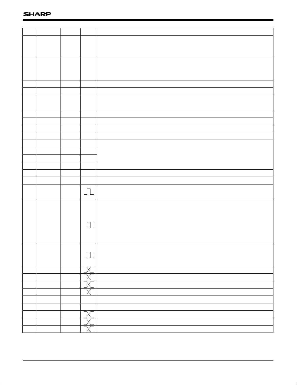
PIN CONNECTIONS
1
2
3
4
5
6
7
8
9
10
11
12
13
14
15
16
17
18
19
20
60
59
58
57
56
55
54
53
52
51
50
49
48
47
46
45
44
43
42
41
21
22
23
24
25
26
27
28
29
30
31
32
33
34
35
36
37
38
39
40
ACL
CKI
CKO
V
DD
GND
ADCK
SCK
SDATA
ADI
9
ADI
8
ADI
7
ADI
6
ADI
5
ADI
4
V
DD
GND
ADI
3
ADI
2
ADI
1
ADI
0
OBCP
ADCLP
BLKX
EEPDA
GND
V
DD
EEPCK
EEPFL
EEPSL
WB1WB
2
MIR
BLC
GNDDA
V
DDDA
V
B
I
REF
V
REF
GNDDA
VIDEO
HD
Y
7
Y6
Y5
Y4
VDD
GND
Y
3
Y2
Y1
Y0
EXCKI
DCK
2
DCK1
VDD
GND
EEMD
3
EEMD2
EEMD1
EEMDS
80
79
78
77
76
75
74
73
72
71
70
69
68
67
66
65
64
63
62
61
FCDS
FS
RS
GND
V
DD
FH
2FH1
FR
GND
V
DD
OFDX
VH
3XVH1X
GND
V
DDV4XV3XV2XV1X
VD
80-PIN LQFP
TOP VIEW
(LQFP080-P-1212)
Page 3
LR38269
3
BLOCK DIAGRAM
ADI9-ADI0
VIDEO
CKI
FR, FH1, FH2
V1X-V4X
VH1X, VH3X
OB
CLAMPING
4 LINES
DELAY
LUMINANCE
SIGNAL
PROCESS
9-BIT DA
COLOR
SIGNAL
PROCESS
SSG
TG
BLKX, CSYNC
HD, VD, ADCLP
OBCP
FCDS, FS, RS
ADCK
CKO
Y7-Y0
DCK1, DCK2
EXCKI
EEPSL, EEPFL
EEPCK, EEPDA
EEMD
2, EEMD3
EEMDS, EEMD
1
WB
1, WB2, MIR, BLC
AUTOMATIC
CONTROL
EEPROM
CONTROL
Page 4
LR38269
4
PIN DESCRIPTION
PIN NO.
SYMBOL I/O DESCRIPTION
1 ACL IC Initializing input.
2 CKI OSCI Input for reference clock oscillation. Connect to CKO (pin 3) with R.
3 CKO OSCO Output for reference clock oscillation. The output is the inverse of CKI (pin 2).
4V
DD – Supply of +3.3 V power.
5 GND – A grounding pin.
6 ADCK OBF6M Clock output of AD converter, connected to pin 13 of IR3Y38M.
7 SCK OBF4M Clock output of serial data, connected to pin 16 of IR3Y38M.
8 SDATA OBF4M Serial data output, connected to pin 19 of IR3Y38M.
9 ADI
9 IC Digital signal input, fed from pin 12 of IR3Y38M (MSB).
10 ADI8 IC Digital signal input, fed from pin 11 of IR3Y38M.
11 ADI
7 IC Digital signal input, fed from pin 10 of IR3Y38M.
12 ADI6 IC Digital signal input, fed from pin 9 of IR3Y38M.
13 ADI
5 IC Digital signal input, fed from pin 8 of IR3Y38M.
14 ADI
4 IC Digital signal input, fed from pin 5 of IR3Y38M.
15 VDD – Supply of +3.3 V power.
16 GND – A grounding pin.
17 ADI
3 IC Digital signal input, fed from pin 4 of IR3Y38M.
18 ADI
2 IC Digital signal input, fed from pin 3 of IR3Y38M.
19 ADI
1 IC Digital signal input, fed from pin 2 of IR3Y38M.
POLARITY
20 ADI0 IC Digital signal input, fed from pin 1 of IR3Y38M (LSB).
21 OBCP OBF4M
Optical clamp pulse output, connected to pin 32 of IR3Y38M.
22 ADCLP OBF4M Clamp pulse output, connected to pin 45 of IR3Y38M.
23 BLKX OBF4M
Blanking pulse output, connected to pin 35 of IR3Y38M.
24 EEPDA IO4MU
Data input from EEPROM output pin.
25 GND – Supply of +3.3 V power.
26 V
DD – A grounding pin.
27 EEPCK IO4MU
Clock output to EEPROM clock input pin.
This pin keeps high-impedance under high level of pin 29.
28 EEPFL IC
Control pin of EEPROM. Connect to the pull-up resistor.
29 EEPSL IC
Control pin of EEPROM. A pull-down resistor should be connected between pin
29 and GND. High level of pin 29 can make data-setting from outside available.
30 WB
1 IO4M
White balance mode setting by both WB1 and WB2.
In digital output mode, pin 30 is assigned to bit 0 (LSB) of U/V signal and pin 31
is assigned to bit 1.
31 WB
2 IO4M
Pin 30
0
0
1
11
0
1
0
Pin 31 White balance mode
AUTO
PRESET WB
1
PRESET WB2
PRESET WB3
Page 5
LR38269
5
PIN NO.
SYMBOL I/O DESCRIPTION
POLARITY
32 MIR IO4M
Video output mode setting.
L : Normal H : Mirror
In digital output mode, this pin is assigned to bit 2 of U/V signal.
33 BLC IO4M
Backlight compensation selection.
L : OFF H : ON
In digital output mode, this pin is assigned to bit 3 of U/V signal.
34 GNDDA – A grounding pin of built-in DA converter.
35 V
DDDA – Supply of +3.3 V power of built-in DA converter.
36 V
B DAO
Bias voltage output of built-in DA converter, connected to GND through a
capacitor.
37 I
REF DAO Bias current output of built-in DA converter, connected to GND through a resistor.
38 V
REF DAI Bias voltage input of built-in DA converter, connected to +1.0 V power supply.
39 GNDDA – A grounding pin of built-in DA converter.
40 VIDEO DAO Analog video signal output.
41 EEMDS IO4MU Electronic exposure mode setting by EEMDS, EEMD1, EEMD2 and EEMD3.
See "Electronic Shutter Speed Setting" in AUTOMATIC CAMERA FUNCTION
CONTROL.
In digital output mode, 41 to 44 pins are assigned to bits 7 to 4 of U/V signals.
42 EEMD
1 IO4MU
43 EEMD
2 IO4MU
44 EEMD3 IO4MU
45 GND – A grounding pin
46 V
DD – Supply of +3.3 V power.
47 DCK
1 OBF4M
Clock output for digital signal output.
Output mode setting switches to CSYNC output.
48 DCK
2 OBF4M
ID pulse output for U/V output signal. In digital output, this pin outputs KEI-
PULSE.
NOTE : KEI-PULSE
At power-on, it keeps low. Both 1/60 s (PAL 1/50 s) as shutter speed and AGC gain
more than data of address 78h sets it high.
49 EXCKI IC
Bit 3 of address 03h sets the function of this pin.
1 : Clock input of 13.5 MHz for digital output
0 : VRI input for analog output
50 Y
0 OBF4M Bit 0 (LSB) of digital luminance signal output.
51 Y1 OBF4M Bit 1 of digital luminance signal output.
52 Y
2 OBF4M Bit 2 of digital luminance signal output.
53 Y3 OBF4M Bit 3 of digital luminance signal output.
54 GND – A grounding pin.
55 V
DD – Supply of +3.3 V power.
56 Y4 OBF4M Bit 4 of digital luminance signal output.
57 Y
5 OBF4M Bit 5 of digital luminance signal output.
58 Y6 OBF4M Bit 6 of digital luminance signal output.
Page 6
LR38269
6
IC : Input pin
OBF4M : Output pin
OBF6M : Output pin
OBF12M : Output pin
IO4M : Input/output pin
IO4MU : Input/output pin with pull-up resistor
OSCI : Input pin for oscillation
OSCO : Output pin for oscillation
DAI : Input pin for DA converter
DAO : Output pin for DA converter
PIN NO.
SYMBOL I/O DESCRIPTION
POLARITY
59 Y7 OBF4M Bit 7 (MSB) of digital luminance signal output
60 HD OBF4M
Horizontal driving pulse output. Either CCD driving timing or BELL-PULSE is
selected by output mode setting.
NOTE : BELL-PULSE
Some period with high level every field.
61 VD OBF4M
Vertical driving pulse output.
Either VD or CSYNC with either driving timing or video output timing is selected
by output mode setting.
62 V
1X OBF4M Vertical driving pulse output, connected to pin 20 of LR36685.
63 V2X OBF4M
64 V3X OBF4M
65 V4X OBF4M
66 VDD – Supply of +3.3 V power.
67 GND – A grounding pin.
68 VH
1X OBF4M Vertical driving pulse output, connected to pin 19 of LR36685.
69 VH
3X OBF4M Vertical driving pulse output, connected to pin 15 of LR36685.
70 OFDX OBF6M OFD driving pulse output, connected to pin 22 of LR36685.
71 V
DD – Supply of +3.3 V power.
72 GND – A grounding pin.
73 FR OBF12M
Reset pulse output, connected to CCD through a capacitor.
74 FH
1 OBF12M Horizontal driving pulse output, connected to CCD.
75 FH2 OBF12M Horizontal driving pulse output, connected to CCD.
76 V
DD – Supply of +3.3 V power.
77 GND – A grounding pin.
78 RS OBF6M
Sample-hold pulse output, connected to pin 31 of IR3Y38M.
79 FS OBF6M
Sample-hold pulse output, connected to pin 30 of IR3Y38M.
80 FCDS OBF6M Sample-hold pulse output, connected to both pin 28 and pin 29 of IR3Y38M.
Vertical driving pulse output, connected to pin 21 of LR36685.
Vertical driving pulse output, connected to pin 18 of LR36685.
Vertical driving pulse output, connected to pin 14 of LR36685.
Page 7

LR38269
7
ADDRESS BIT CONTENTS
00h Not used
INTERNAL COEFFICIENT TABLE
NAME
7
MODE 1
TV mode 0 : NTSC 1 : PAL
01h
02h Luminance gamma selection
MODE 2
7-6
7
MODE 3
Polarity selection of SP
1 and SP203h
04h Exposure reference level (target of exposure control)
REF_IRIS1
7-0
7-0UW_E5 Exposure control weighting factor 50Ch
7-0UW_E4 Exposure control weighting factor 40Bh
7-0UW_E3 Exposure control weighting factor 30Ah
7-0UW_E2 Exposure control weighting factor 209h
7-0UW_E1 Exposure control weighting factor 108h
7-0
REF_IRIS2
Exposure reference level with backlight compensation07h
7-0CTLD_02 Lower level of exposure reference level06h
7-0CTLD_01 Higher level of exposure reference level05h
12h Bottom-right point of exposure window areaCWA_E 6-0
11h Top-left point of exposure window areaCWP_E 6-0
10h Weighting factor of exposure window areaCW_E 6-0
0Fh Exposure control weighting factor 8UW_E8 7-0
0Eh Exposure control weighting factor 7UW_E7 7-0
0Dh Exposure control weighting factor 6UW_E6 7-0
6
5
4
3
2
1
0
Input signal delay 0 : No delay 1 :
1 clock cycle delay
Clock polarity to latch input signal 0 : Normal 1 : Inverted
YL killer 0 : Normal 1 : Killed
Pin mode selection (NOTE 1) 0 : Mode input 1 : U/V output
VD output timing selection (NOTE 1)
HD output timing selection 0 : TG 1 : Video output
DCK
1 output selection (NOTE 1)
5-4
3
2
1
0
Color gamma selection
Vertical aperture enhancement 0 : ON 1 : OFF
Horizontal aperture enhancement 0 : ON 1 : OFF
Color killer 0 : ON 1 : OFF
Flicker reduction 0 : ON 1 : OFF
Polarity inverter of HG
Video format selection 0 : Interlace 1 : Non-interlace
UV dot-sequence selection (output stage)
UV dot-sequence selection
Carrier balance tuning 0 : ON 1 : OFF
AGC 0 : Auto 1 : Fixed (gain at
address 1Bh)
Digital output clock 0 : 9.6 MHz 1 :
Clock of EXCKI pin
6
5
4
3
2
1
0
Page 8

LR38269
8
ADDRESS BIT CONTENTSNAME
Electronic shutter speed pitch 000 : Slower 111 : Quicker
Maximum luminance level factor to control exposure
Minimum luminance level factor to control exposure
Integrated pixels of peak signal 0 : 8 pixels 1 : 4 pixels
Condition of exposure control under locking-in number of images to control exposure.
0 : 1 image 1 :
Integrated 3 images
Valid image to control exposure 00 : Every image
01 : Every 2 images 10 : Every 4 images 11 : Every 8 images
Condition of exposure control under free-running
Number of images 0 : 1 image 1 :
Integrated 3 images
Valid image to control exposure 00 : Every image
01 : Every 2 images 10 : Every 4 images 11 : Every 8 images
AGC control data 000 : Slower 111 : Quicker
Minimum pitch of AGC variable gain
DATA should be between 01h (finest pitch) and 1Fh.
Not used
AGC gain at power-on
AGC reference gain (more than data of 19h)
Fixed AGC gain
AGC maximum gain
Offset control 0 : Auto 1 : Fixed
13h
EE_DIV_STP
6-4
14h
P_HEE_IRIS
7-0
15h
P_LEE_IRIS
7-0
16h
INT_PEAK
6
IRIS_DLY1
5
4
3
IRIS_DLY2
2
1
0
17h
AG_DIV_STP
7-5
AG_GAIN 4-0
18h
19h
I_AGC_D8
7-0
1Ah
REF_AGC_D8
7-0
1Bh
S_38M_GA
7-0
1Ch
S_38M_MAX
2-0
1Dh
S_38M_OFS
6
1Eh CSEPR 7-0
1Fh CSEPB 7-0
20h CB_R 7-0
21h CB_B 7-0
22h K_T_R 7-0
23h K_T_B 7-0
24h
MAX_WBR
7-0
25h
MIN_WBR
7-0
26h
MAX_WBB
7-0
27h
MIN_WBB
7-0
28h WBR1 7-0
29h WBB1 7-0
2Ah WBR2 7-0
2Bh WBB2 7-0
2Ch WBR3 7-0
Coefficient to extract red color signal
Coefficient to extract blue color signal
Red signal carrier balance
Blue signal carrier balance
Basic red WB gain
Basic blue WB gain
Red WB gain at maximum color temperature
Red WB gain at minimum color temperature
Blue WB gain at minimum color temperature
Red WB data (preset 3)
Blue WB gain red at maximum color temperature
Red WB data (preset 1)
Blue WB data (preset 1)
Red WB data (preset 2)
Blue WB data (preset 2)
LPFE_F
3-2 Exposure response speed selection with flicker reduction
00 : Slower 01 : Normal 10 or 11 : Quicker
LPFE_N
1-0 Exposure response speed selection
00 : Slower 01 : Normal 10 or 11 : Quicker
Offset data5-0
Page 9

LR38269
9
ADDRESS BIT CONTENTSNAME
2Dh WBB3 7-0 Blue WB data (preset 3)
2Eh K_GA_R 7-0 Correction coefficient of R – Y gain
2Fh
K_GA_B 7-0 Correction coefficient of B – Y gain
30h
REF_GA_R
5-0 Basic gain of R – Y signal
31h
REF_GA_B
5-0 Basic gain of B – Y signal
32h GA_R1 5-0 R – Y gain data (preset 1)
33h GA_B1 5-0 B – Y gain data (preset 1)
34h GA_R2 5-0 R – Y gain data (preset 2)
35h GA_B2 5-0 B – Y gain data (preset 2)
36h GA_R3 5-0 R – Y gain data (preset 3)
37h GA_B3 5-0 B – Y gain data (preset 3)
38h
MAX_IQAREA
7 AWB IQ area selection 0 : Set data 1 : Widest
39h
AWB_WAIT_C
7-0 AWB time constant after lock-in (lower 8 bits)
3Ah CMP_CT 7-0 Valid data to control AWB (01h makes all AWB data valid.)
3Bh
AWB_HCL
7-0 Highest luminance level to be available for AWB control
3Ch AWB_LCL 7-0 Lowest luminance level to be available for AWB control
3Dh
REF_WBPK
7-0 Offset luminance level to control data of 3Bh and 3Ch
3Eh K_CL 7-0 Maximum luminance level factor to control data of 3Bh and 3Ch
3Fh K_WBCL 7-0 Weighting factor for data of 3Dh and 3Eh
40h
UW_IQ1 7-0 AWB control weighting factor 1
41h UW_IQ2 7-0 AWB control weighting factor 2
42h UW_IQ3 7-0 AWB control weighting factor 3
43h UW_IQ4 7-0 AWB control weighting factor 4
44h
INT_I_R – Y
7 AWB control data 0 : I/Q 1 : R – Y/B – Y
45h
CWPA_IQ
7-4 Top-left point of AWB window area
46h
CTLD_AW0
7-0 Exposure level to erase the area to detect white color
LPFIQ_F
6-5 Response speed selection with flicker reduction
00 : Slower 01 : Normal 10 or 11 : Quicker
LPFIQ_N 4-3 Response speed
FINE 2 Fine-tuning mode of auto white balance
AWB_WAIT_C
1-0 AWB time constant after lock-in (upper 2 bits)
Weighting factor of AWB window area6-0CW_IQ
3-0 Bottom-right point of AWB window area
Page 10

LR38269
10
ADDRESS BIT CONTENTSNAME
47h
AWB_IP_L
7-0 First AWB detector area I-PLUS
48h
AWB_IM_L
7-0 First AWB detector area I-MINUS
49h
AWB_QP_L
7-0 First AWB detector area Q-PLUS
4Ah
AWB_QM_L
7-0 First AWB detector area Q-MINUS
4Bh
AWB_IP_S
7-0 Second AWB detector area I-PLUS
4Ch
AWB_IM_S
7-0 Second AWB detector area I-MINUS
4Dh
AWB_QP_S
7-0 Second AWB detector area Q-PLUS
4Eh
AWB_QM_S
7-0 Second AWB detector area Q-MINUS
4Fh
AWB_I_WH_L
6-0 First AWB white zone I-PLUS
50h
AWB_Q_WH_L
6-0 First AWB white zone Q-PLUS
51h
AWB_I_WH_S
6-0 Second AWB white zone I-MINUS
52h
AWB_Q_WH_S
6-0 Second AWB white zone Q-MINUS
53h K_MAT_R 7-0 R – Y gain factor for color matrix correction
54h K_MAT_B 7-0 B – Y gain factor for color matrix correction
55h
REF_MAT_R
5-0 Basic R – Y data of color matrix correction
56h
REF_MAT_B
5-0 Basic B – Y data of color matrix correction
57h MAT1 7-0 Color matrix data (preset 1) R – Y 4 bits, B – Y 4 bits
58h MAT2 7-0 Color matrix data (preset 2) R – Y 4 bits, B – Y 4 bits
59h MAT3 7-0 Color matrix data (preset 3) R – Y 4 bits, B – Y 4 bits
5Ah
COL_S 7-0 AGC gain to start suppressing color signal
5Bh COL_H 5-0 Pitch of color signal suppressing by address 5Ah
5Ch CKI_HCL 7-0 Higher luminance level to start suppressing color signal
5Dh CKI_LCL 7-0 Lower luminance level to start suppressing color signal
5Eh
CKI_HLGA
7-4 Color signal suppression gain for higher luminance signal
5Fh
CKI_HLTI
7-4 Highlight luminance signal position to suppress color –2 to +2
60h
CKI_HECL
7-0 Horizontal aperture level to start suppressing color signal
61h
CKI_EVCL
7-0 Vertical aperture level to start suppressing color signal
62h
CKI_EGA
7-4 Horizontal aperture gain to suppress color signal by address 60h
63h APT_S 7-0 AGC gain to start suppressing aperture signal
64h APT_H 5-0 Gain to suppress aperture signal by address 63h
65h NSUP_R 7-0 R – Y signal coring level
66h NSUP_B 7-0 B – Y signal coring level
67h CKI_IEL 7 Color-killer level 0 : Unity gain 1 : 1/4 gain
68h
APT_HTIM
7-6 Horizontal aperture signal position –1 to +1
NOTE :
Data to set first area should be larger than
data to set second area.
Second area should be closer to the cross
point of I-axis and Q-axis, compared to first
area.
Color signal suppression gain for lower luminance signal
Lowest luminance signal position to suppress color –2 to +2
Vertical aperture gain to suppress color signal by address 61h
Horizontal edge signal position to kill color signal –2 to +2
Vertical edge signal position to kill color signal –2 to +2
6-4
3-1
APT_HGA
5-1 Horizontal aperture gain
CKI_ETI
3-0
3-0
3-0
Page 11

LR38269
11
ADDRESS BIT CONTENTSNAME
6Fh
TG_SEL1
7-5 ADCK phase setting (6 steps per 60˚)
70h
TG_SEL2
7-5 FCDS phase setting (±2 ns x 3)
71h
ENC_MUTE
7 Encoder muting 0 : OFF 1 : ON
72h
SYNC_LEV
7-0 SYNC level (80h = 40 IRE)
73h BAS_R 7-0 BURST level of R – Y
74h BAS_B 7-0 BURST level of B – Y
75h
MUTE_OUT
7 Muting at power-on
76h TEST 2-0 Test data (EEPROM data must be 00h)
77h VRI 2 EXCKI pin function 1 : VRI function 0 : Clock input
78h KEI_AGC 8 AGC gain to set KEI-PULSE high
(NOTE 1)
ADDRESS
01
SIGNAL OUTPUT
HD (Pin 60)
HD
HD
HD
HD
HD
BELL
BELL
VD (Pin 61)
VD for video out
VD for CCD driving
CSYNC
VD for video out
VD for CCD driving
VD for video out
VD for CCD driving
DCK
1 (Pin 47)
DCK
1
DCK1
DCK1
CSYNC
CSYNC
CSYNC
CSYNC
Bit 0
0
0
1
0
0
1
1
Bit 2
1
0
x
1
0
1
0
Bit 3
DIGITAL
1
ANALOG
0
69h APT_HCL 6-0 Horizontal aperture signal coring
6Ah APT_VGA 4-0 Vertical aperture gain
6Bh
APT_VCL 6-0 Vertical aperture signal coring
6Ch CBLK_LV 7 CBLK level selection 0 : 00h 1 : 10h
6Dh VARI_Y 4-0 luminance signal position
6Eh
SW_CTRL
7-0
The following setting is available under both EEPSL = H and digital output mode
WB1 (LSB), WB2, BACK, EEMDS, EEMD1 EEMD2, EEMD3, MIR (MSB)
Set up level6-1SETUP
FS phase setting (±2 ns x 3)
FR phase setting (±2 ns x 3)
4-2
4-2
SYNC adder 0 : ON 1 : OFF
Serial digital data setting
Gain of video output amplifier
6
5
4-0
SYNC_SW
SEL_RB
OUT_GAIN
Muting period (data multiplied by 1 field period)6-0
Test data (EEPROM data must be 0)
Test data (EEPROM data must be 0)
1
0
TEST
TEST
Page 12

LR38269
12
VOH1Output "High" voltage 0.8 VDDIOH = –4 mA V
Output "Low" voltage V
OL1 0.2 VDDIOL = 4 mA V
ABSOLUTE MAXIMUM RATINGS
RECOMMENDED OPERATING CONDITIONS
PARAMETER SYMBOL
Power supply voltage V
DD
Input voltage VI
ELECTRICAL CHARACTERISTICS (VDD = 3.0 to 3.6 V, TOPR = –20 to +70 ˚C)
Input "Low" voltage VIL
Input "High" voltage VIH
Input "Low" current |IIL1|
Output "Low" voltage V
OL2
Output "High" voltage VOH2
Output "Low" voltage VOL3
Output "High" voltage VOH3
Resolution RES
Linearity error EL
Differential error ED
Full scale current |I
FS|
Reference voltage VREF
Reference resistance RREF
Output load resistance ROUT
PARAMETER SYMBOL CONDITIONS MIN.
0.8 V
DD
0.8 VDD
0.8 VDD
4.8
75
9
13
100
TYP.
1.0
MAX.
0.2 V
DD
±1.0
±3.0
0.2 V
DD
0.2 VDD
VIN = 0 V
V
REF = 1.0 V
RREF= 4.8 k$
R
OUT = 75 $
I
OH = –12 mA
IOL = 12 mA
I
OH = –6 mA
IOL = 6 mA
$
V
V
V
V
bit
LSB
LSB
mA
V
V
µA
V
UNITk$NOTE
2
1
3
4
–0.3 to V
DD + 0.3
–0.3 to +4.3
RATING UNIT
V
V
˚C–55 to +150T
STGStorage temperature
V–0.3 to V
DD + 0.3VOOutput voltage
PARAMETER SYMBOL
Power supply voltage V
DD
Operating temperature TOPR –20
3.0
MIN. UNIT
V
˚C
MHzfCKInput clock frequency 28.6
TYP. MAX.
3.3 3.6
+25 +70
5
8
7
7
9
NOTES :
1. Applied to inputs (IC, IO4M, IO4MU).
2. Applied to input (IO4MU).
3. Applied to outputs (OBF4M, IO4M, IO4MU).
4. Applied to output (OBF6M).
5. Applied to output (OBF12M).
6. Applied to output (OSCO).
7. Applied to output (VIDEO).
8. Applied to input (V
REF).
9. Applied to output (I
REF).
6
V
VI
OL = 3 mA
IOH = –2 mA
0.2 VDD
0.8 VDDVOH4Output "High" voltage
VOL4Output "Low" voltage
Page 13

LR38269
13
Data Interface
(1) Format of data transfers
• Format of transfers : Asynchronous (Based on
RS-232C standard)
• Bit rate : 9 600 bps
• Data length : 8 bits
• Parity check : 1 even parity bit
• Start bit : 1 bit
• Stop bit : 1 bit
• Signal voltage level (CMOS)
• System configuration
3.3 V
GND LSB MSB
RxD
D
0 D1 D2 D3 D4 D5 D6 D7
Even
Parity
Bit
Data Bit
Stop
Bit
Start
Bit
LR38269
Dedicated
Adjustment
Tool
by SHARP
PC with
Windows
RxD
TxD
SCK
SDATA
SLDI
SCK
SDATA
SLDI
DSP Address DSP Data
5.8 µs
11.6 µs
1.4 µs
Page 14

LR38269
14
AUTOMATIC CAMERA FUNCTION CONTROL
Automatic Electronic Exposure Control
Electronic shutter speed is controlled so that the
exposure control data approach to the data of
address 04h.
Under BLC mode, the data of address 07h is
available instead of address 04h.
After the exposure control data is less than the data
of address 05h, an electronic shutter speed is hold.
And then AGC gain is controlled so that the
exposure control data will be less than the data of
address 06h.
In the case of coming more than the data of
address 07h, exposure control starts again.
Electronic Shutter Speed Setting
By either hardware or coefficient data, electronic
shutter speed below is selectable.
EEMDS EEMD1 EEMD2 EEMD3
ELECTRONIC SHUTTER SPEED
NTSC PAL
00001/60 s 1/50 s
00011/100 s 1/120 s
00101/250 s 1/250 s
00111/500 s 1/500 s
01001/1 000 s 1/1 000 s
01011/2 000 s 1/2 000 s
01101/5 000 s 1/5 000 s
01111/10 000 s 1/10 000 s
10001/20 000 s 1/20 000 s
10011/50 000 s 1/50 000 s
10101/100 000 s 1/100 000 s
10111/30 s 1/25 s
11001/15 s 1/12.5 s
11011/7.5 s 1/6.25 s
1110
AUTO
1/60 to 1/100 000 s
AUTO
1/50 to 1/100 000 s
1111
AUTO
1/60 to 1/100 000 s
AUTO
1/50 to 1/100 000 s
Slower shutter speed less than 1/60 s (1/50 s of
PAL) can make images whose interval is every two
fields, every four fields, etc..
VD pulse is also converted to the same frequency
as the output image rate.
Page 15

Electronic exposure control data comes from below
equation using averaged luminance levels of 64
areas in one image, made by DSP.
Electronic exposure control data =
[{Weighted data 1 q x (64 – address 10h)
+ weighted data 2 w x address 10h} ÷ 64
x (256 – address 14h – address 15h)
+ top level e x address 14h
+ bottom level r x address 15h] ÷ 256
q Weighted data 1
This comes from the following equation weighting in
horizontal.
Weighting factors are the data from address 08h to
address 0Fh.
{(Y
11 + Y12 π + Y18) ÷ 8 x address 08h
+ (Y
21 + Y22 π + Y28) ÷ 8 x address 09h
:
+ (Y
81 + Y82 π + Y88) ÷ 8 x address 0Fh} ÷ 256
= Weighted data 1
The sum from address 08h to address 0Fh shall be
256.
w Weighted data 2
Weighting area can be set by the data of address
11h and address 12h. (see "NOTES" in Gamma
Characteristic Option)
This comes from the following equation weighting in
selected areas.
(Y
33 + Y34 π + Y66)/number of areas to be selected
= Weighted data 2
e Top level : The highest luminance data in one
image by averaging either 4 pixels
or 8 pixels in horizontal.
r Bottom level : The lowest luminance data in
one image by averaging either 4
pixels or 8 pixels in horizontal.
Auto White Balance Control
White balance control data less than the data of
address 51h and address 52h stops AWB.
White balance control data less than the data of
address 4Fh and address 50h makes AWB active
so that white balance control data is less than the
data of address 51h and address 52h.
In the case of larger than the data of address 4Fh
and address 50h, AWB will be active again.
White balance data comes from the following
equation using averaged I and Q data of 16 areas
in one image.
White balance data =
{Weighted data 3 q x (64 – address 44h)
+ weighted data 4 w x address 44h} ÷ 64
LR38269
15
Y11 Y12 Y13 Y14 Y15 Y16 Y17 Y18
Y21 Y22 Y23 Y24 Y25 Y26 Y27 Y28
Y31 Y32 Y33 Y34 Y35 Y36 Y37 Y38
Y41 Y42 Y43 Y44 Y45 Y46 Y47 Y48
Y51 Y52 Y53 Y54 Y55 Y56 Y57 Y58
Y61 Y62 Y63 Y64 Y65 Y66 Y67 Y68
Y71 Y72 Y73 Y74 Y75 Y76 Y77 Y78
Y81 Y82 Y83 Y84 Y85 Y86 Y87 Y88
I11 I12 I13 I14
I21 I22 I23 I24
I31 I32 I33 I34
I41 I42 I43 I44
Q11 Q12 Q13 Q14
Q21 Q22 Q23 Q24
Q31 Q32 Q33 Q34
Q41 Q42 Q43 Q44
Page 16

q Weighted data 3
I (or Q) data comes from the following equation
using the weighting data from address 40h to
address 43h.
{(I
11 + I12 π + I14) ÷ 4 x address 40h
+ (I
21 + I22 π + I24) ÷ 4 x address 41h
:
+ (I
41 + I42 π + I44) ÷ 4 x address 43h} ÷ 256
= Weighted data 3
The sum from the data of address 40h to the data
of address 43h shall be 256.
w Weighted data 4
Weighting area can be selected by address 45h.
(see "NOTES" in Gamma Characteristic Option.)
Weighted data comes from averaged data in
selected area.
e White balance area setting
The sum of I and Q can be regulated by the
luminance level and the color level.
Setting target zone : address 47h to address 4Ah
White balance data less than the data of address
51h and address 52h changes the target zone of
auto white balance to the zone by the data from
address 4Bh to 4Eh.
Above regulation comes from the following equation
along the luminance level.
Setting available luminance level range :
Highest luminance level limiter =
address 3Bh + [{address 3Eh x H peak level +
(256 – address 3Eh) x exposure control data} ÷
256 – address 3Dh] x address 3Fh
Lowest luminance level limiter =
address 3Ch + [{address 3Eh x H peak level +
(256 – address 3Eh) x exposure control data} ÷
256 – address 3Dh] x address 3Fh
Auto Color Matrix Compensation
Color matrix compensation can be done by
R – Y = R – Y ± (Data 1 x B – Y)
B – Y = B – Y ± (Data 2 x R – Y)
Above data comes from below equation along the
variation of color temperature.
Data 2 =
address 55h + {(working R white balance data –
address 25h + (address 26h – working B white
balance data)} ÷ 32 x address 53h ÷ 8
Data 2 =
address 56h + {(working R white balance data –
address 25h) + (address 26h – working B white
balance data)} ÷ 32 x address 54h ÷ 8
Auto Color Level Compensation
Color level can be auto-controlled by the following
equation along the variation of color temperature.
B – Y level =
address 30h + {(working R white balance data –
address 25h) x address 22h + (address 26h –
working B white balance data) x address 23h} ÷ 32
x address 2Eh ÷ 8
R – Y level =
address 31h + {(working R white balance data –
address 25h) x address 22h + (address 26h –
working B white balance data) x address 23h} ÷ 32
x address 2Fh ÷ 8
LR38269
16
Page 17

LR38269
17
Color Level Suppression Under Lower
Illuminance
Working AGC gain can control both R – Y level
and B – Y level by the following equation.
R – Y level =
address 31h x {16 – (working AGC gain – address
5Ah) x address 5Bh ÷ 16} ÷ 16
B – Y level =
address 30h x {16 – (working AGC gain – address
5Ah) x address 5Bh ÷ 16} ÷ 16
{16 – (working AGC gain – address 5Ah) x
address 5Bh ÷ 16} ≤ 16
When (working AGC gain – address 5Ah) ≤ 0, ( ) = 0.
Aperture Level Suppression Under
Illuminance
Working AGC gain can control both the horizontal
aperture level and the vertical aperture level by the
following equation.
Horizontal aperture level =
address 68h x {16 – (working AGC gain – address
63h) x address 64h ÷ 16} ÷ 16
Vertical aperture level =
address 6Ah x {16 – (working AGC gain – address
63h) x address 64h ÷ 16} ÷ 16
{16 – (working AGC gain – address 63h) x
address 64h ÷ 16} ≤ 16
When (working AGC gain – address 63h) ≤ 0, ( ) = 0.
Page 18

LR38269
18
Gamma Characteristic Option
(1) Luminance Signal Gamma Option
Bit 7 and bit 6 of address 02h can select one out of
4 responses below.
00
01
10
11
256
224
192
160
128
INPUT
96
64
32
0
64
0
128
192
256
OUTPUT
320
384
448
512
576
640
896
832
768
704
960
(2) Color Signal Gamma Option
Bit 5 and bit 4 of address 02h can select one out of
4 responses below.
00
01
10
11
256
224
192
160
128
96
64
32
0
64
0
128
192
256
320
384
448
512
576
640
896
832
768
704
960
INPUT
OUTPUT
Page 19

LR38269
19
NOTES :
• Weighting position of auto electronic exposure control (address 11h)
• Weighting area of auto electronic exposure control (address 12h)
00h 08h · 30h 38h
39h
·
3Eh
3Fh
31h
·
36h
37h
·
·
·
·
09h
·
0Eh
0Fh
01h
·
06h
07h
00h 08h · 30h 38h
39h
·
3Eh
3Fh
31h
·
36h
37h
·
·
·
·
09h
·
0Eh
0Fh
01h
·
06h
07h
• Weighting position of auto white balance control (address 45h)
00h 04h 08h 0Ch
0Dh
0Eh
0Fh
09h
0Ah
0Bh
05h
06h
07h
01h
02h
03h
00h 04h 08h 0Ch
0Dh
0Eh
0Fh
09h
0Ah
0Bh
05h
06h
07h
01h
02h
03h
• Weighting area of auto white balance control (address 45h)
Page 20

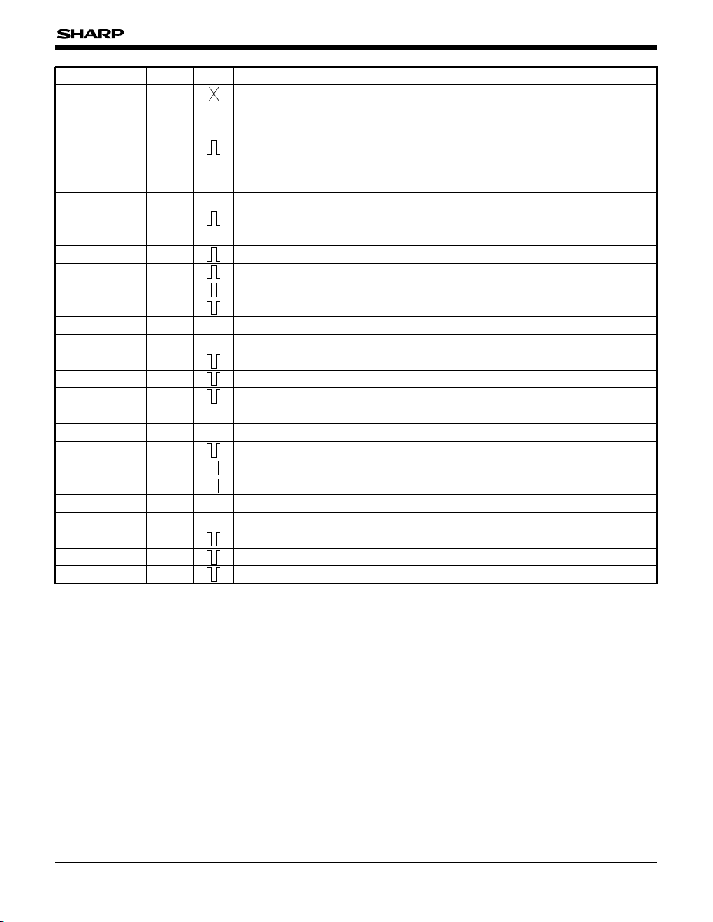
PACKAGES FOR CCD AND CMOS DEVICES
20
PACKAGE (Unit : mm)
1
0.1
±0.1
Package
base plane
60
0.5
TYP.
0.2
±0.08
41
40
(1.0)
12.0
±0.2
21
(1.0)
20
(1.0)
(1.0)
12.0
±0.2
14.0
±0.3
61
80
13.0
±0.2
M0.08
0.10
0.125
±0.05
0.6375
1.40
±0.2
14.0
±0.3
1.70
MAX.
80 LQFP (LQFP080-P-1212)
 Loading...