

Page 1
In the absence of confirmation by device specification sheets, SHARP takes no responsibility for any defects that may occur in equipment using any SHARP devices shown in
catalogs, data books, etc. Contact SHARP in order to obtain the latest device specification sheets before using any SHARP device.
1
DESCRIPTION
The LR36685 is a CMOS vertical clock driver and
shutter driver IC for CCD area sensors which
provides the functions to convert the voltage and
impedance from the CMOS level.
FEATURES
• Built-in seven circuits
– 2-level output :
2 circuits for vertical CCD clock driver
Output voltage level (TYP.) = –9 to 0 V
– 3-level output :
4 circuits for vertical CCD clock driver
Output voltage level (TYP.) = –9 to 0 to +15 V
– 2-level output :
1 circuit for shutter driver
Output voltage level (TYP.) = –9 to +17 V
• Switchable between NTSC (EIA) and PAL (CCIR)
modes
• Package :
24-pin SSOP (SSOP024-P-0275)
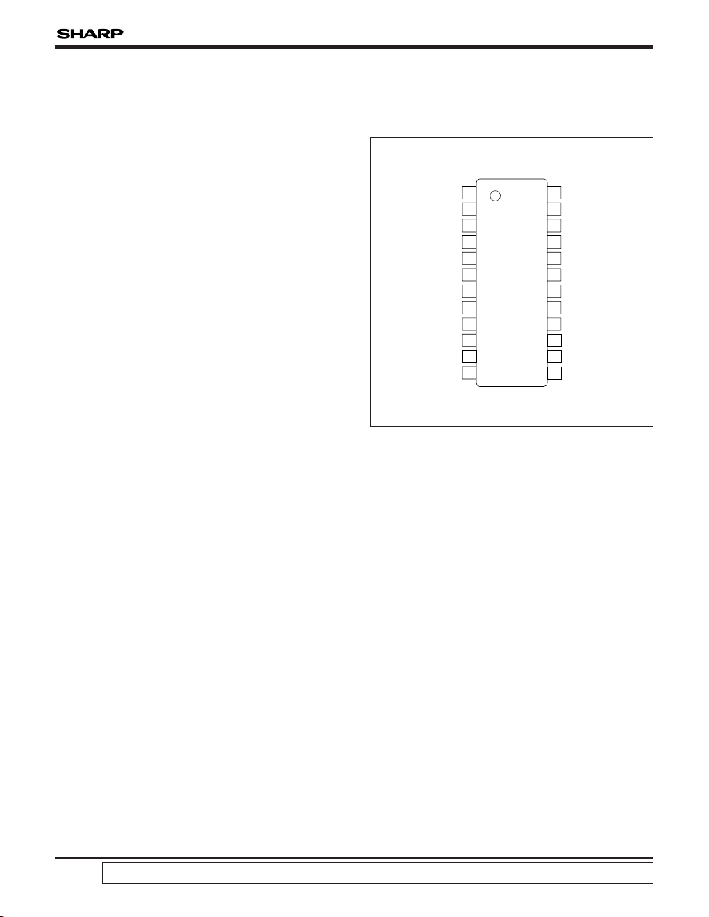
PIN CONNECTIONS
LR36685
LR36685
Vertical Driver IC for
CCD Area Sensors
POFD
VH
1BX
1
24
23
22
21
20
19
18
17
16
15
14
13
VMb
V4X
2
VL
VH3AX
3
V2
GND
4
V4
VDD
5
NC
V
3X
6
V3B
VH1AX
7
V3A
V1X
8
V1B
V2X
9
V1A
OFDX
10
VMa
VH3BX
11
VH
VOFDH
12
24-PIN SSOP
TOP VIEW
(SSOP024-P-0275)
Page 2
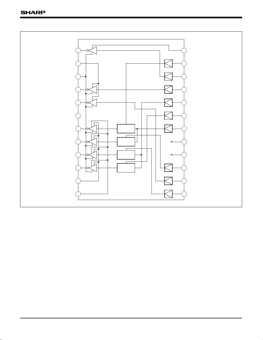
LR36685
2
BLOCK DIAGRAM
VOFDH
VH3BX
OFDX
V
2X
V1X
VH1AX
V3X
VDD
GND
VH
3AX
V4X
VH1BX
POFD
V
Mb
VL
V2
V4
NC
V
3B
V3A
V1B
V1A
VMa
VH
MIX
MIX
MIX
MIX
24
23
22
21
20
19
18
17
16
15
14
13
1
2
3
4
5
6
7
8
9
10
11
12
Page 3
LR36685
3
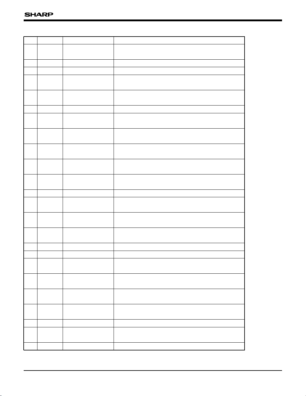
PIN DESCRIPTION
16 GND Ground A grounding pin.
PIN NO.
SYMBOL PIN NAME DESCRIPTION
1 POFD OFD pulse output
An electronic shutter pulse output.
(high level = V
OFDH, low level = VL)
2VMb Power supply A power supply for high level of V2 and V4.
3V
L Power supply A power supply for low level of all output pulses.
4V
2
Vertical transfer
pulse output 2
A pulse to drive vertical CCD shift register.
Connect to Ø
V2.
5V
4
Vertical transfer
pulse output 4
A pulse to drive vertical CCD shift register.
Connect to Ø
V4.
6 NC No connection No connection
A pulse to drive vertical CCD shift register.
Connect to Ø
V3B.
Vertical transfer
pulse output 3B
V
3B7
9V
1B
Vertical transfer
pulse output 1B
A pulse to drive vertical CCD shift register.
Connect to ØV1B.
8V
3A
Vertical transfer
pulse output 3A
A pulse to drive vertical CCD shift register.
Connect to Ø
V3A.
A pulse to drive vertical CCD shift register.
Connect to Ø
V1A.
Vertical transfer
pulse output 1A
V
1A10
11 V
Ma Power supply
A power supply for intermediate level of V
1A, V1B, V3A
and V3B.
A power supply for high level of V1A, V1B, V3A and V3B.Power supplyVH12
13 VH
1BX
Readout pulse input1BA pulse that transfers the charge of the photo-diode to
the vertical shift register.
A vertical transfer pulse input.
Vertical transfer
pulse input 4
V
4X14
15 VH
3AX
Readout pulse input3AA pulse that transfers the charge of the photo-diode to
the vertical shift register.
A vertical transfer pulse input.
Vertical transfer
pulse input 3
V
3X18
A power supply for input pulses.Power supplyV
DD17
19 VH
1AX
Readout pulse input1AA pulse that transfers the charge of the photo-diode to
the vertical shift register.
A vertical transfer pulse input.
Vertical transfer
pulse input 1
V
1X20
22 OFDX OFD pulse input An electronic shutter pulse input.
21 V
2X
Vertical transfer
pulse input 2
A vertical transfer pulse input.
A pulse that transfers the charge of the photo-diode to
the vertical shift register.
Readout pulse input
3B
VH
3BX23
24 V
OFDH Power supply A power supply for high level of POFD.
Page 4

LR36685
4
ABSOLUTE MAXIMUM RATINGS (TA = +25 ˚C)
RECOMMENDED OPERATING CONDITIONS
PARAMETER SYMBOL RATING UNIT
Supply voltage
V
DD GND – 0.3 to GND + 6.0 V
V
H – VL 29.0 V
VMa, VMb VL to VH V
V
OFDH
– V
L
34.0 V
Input voltage VIN GND – 0.3 to VDD + 0.3 V
Storage temperature T
STG –55 to +150 ˚C
1
NOTE
NOTE :
1. VH (MIN.) = VDD, VOFDH (MIN.) = VDD, VL (MAX.) = GND
PARAMETER SYMBOL MIN. TYP.
Supply voltage
V
DD 3.0 3.3
V
H – VL 17.0 24.0
V
H 12.0 15.0
VL –10.0 –9.0
V
Ma, VMb 0.0
V
OFDH
– VL17.0 26.0 V
V
V
V
V
V
UNIT
32.0
–5.0
20.0
27.0
5.5
MAX.
+70 ˚C–20T
OPROperating temperature
kHz15.625PAL
kHz15.734NTSC
Operating frequency
0.25V
DD
V0VIN (Low)
Input voltage
24.0 V17.012.0V
OFDH
VIN (High) 0.8VDD V
VDD+ 0.2
Page 5

LR36685
5
ELECTRICAL CHARACTERISTICS
DC Characteristics
(VDD = +3.3 V, VH = +15.0 V, VL = –9.0 V, VMa = VMb = 0 V, VOFDH = +17.0 V, TA = +25 ˚C)
Input "Low" voltage VIL
Input "High" voltage VIH
Input "Low" current |IIL|
|IIH|
Output "Low" voltage V
OL
Output "High" voltage VOH
Output "Intermediate" voltage
V
OMLa
VOMHa
VOMLb
VOMHb
Output "Low" current |IOL|
Output "High" current |I
OH|
Output "High" current |IOFDH|
Output "Intermediate" current
|I
OMLa|
|I
OMHa|
|IOMLb|
|I
OMHb|
RONH
RONOFH
RONM
RONL
|IDD|
PARAMETER SYMBOL CONDITIONS
Input "High" current
V
OFDHOutput "High" voltage
MIN.
0.8V
DD
0.0
1.0
1.0
1.0
1.0
1.0
1.0
1.0
–0.1
–0.1
–0.1
–0.1
16.9
14.9
20
25
20
TYP.30MAX.
1.0
200
VDD+ 0.2
0.25V
DD
0.1
0.1
0.1
0.1
–8.9
2.0
I
OL < 1 µA
V
IH = 3.3 V
VIL = 0 V
I
OFDH = 20 mA
I
OH = 20 mA
VOMHb = VM + 0.1 V
V
OMLb = VM – 0.1 V
VOMHa = VM + 0.1 V
V
OMLa = VM – 0.1 V
V
OFDH = VOFDH – 0.1 V
VOH = VH – 0.1 V
V
OL = VL + 0.1 V
IOMHb < 1 µA
I
OMLb < 1 µA
I
OMHa < 1 µA
IOMLa < 1 µA
I
OFDH < 1 µA
IOH < 1 µA
I
OL = 20 mA
IOM = 20 mA $
$
mA
V
V
V
V
V
V
V
mA
mA
mA
mA
mA
mA
V
V
µA
µA
$
UNIT
$3
NOTE
3
1, 2, 3
1
2
1, 2, 3
1, 2, 3
µA
µA200
200|I
L|
|I
M|
µA
µA200
200|IOFDH|
|I
H|
2
3
Static current
Output ON resistance
mA
2
2
1
2
1, 2
NOTES :
1. Applied to outputs (V2, V4).
2. Applied to outputs (V
1A, V1B, V3A, V3B).
3. Applied to output (POFD).
Page 6

LR36685
6
AC Characteristics
(VDD = +3.3 V, VH = +15.0 V, VL = –9.0 V, VMa = VMb = 0 V, VOFDH = +17.0 V, TA = +25 ˚C,
Shutter speed : 1/100 000 s)
PARAMETER SYMBOL CONDITIONS TYP.
Sequential delay
t
TRM
(VL/VM)
V
IN to VM – 1.0 V
(V1A, V1B, V2, V3A, V3B, V4)
600 ns
UNIT
1 200
MAX.
Dynamic current
t
TFOFDL
(V
OFDH/VL
)
tTROFDH
(VL/V
OFDH
)
tTFM
(VH/VM)
t
TRH
(VM/VH)
t
TFL
(VM/VL)
160 ns80
V
IN to VL + 1.0 V
(POFD)
160 ns80
V
IN to VOFDH – 1.0 V
(POFD)
1 600 ns800
V
IN to VM + 1.0 V
(V1A, V1B, V3A, V3B)
1 600 ns800
V
IN to VH – 1.0 V
(V
1A, V1B, V3A, V3B)
1 200 ns600
V
IN to VL + 1.0 V
(V1A, V1B, V2, V3A, V3B, V4)
During operation 5 mA10IDYN
NOTE :
Refer to "Switching Characteristics Conditions" and "Equivalent Circuit".
Page 7

LR36685
7
Switching Characteristics Conditions
Equivalent Circuit
(While V1A and V3A [or V1B and V3B] are measured, V1B and V3B
[or V1A and V3A] are open.)
tTRH tTFM
tTFL
tTRM
VM – 1.0
V
H – 1.0
V
M + 1.0
V
L + 1.0
V
L + 1.0
tTROFDH tTFOFDL
VDD (3.3 V)
GND (0.0 V)
V
DD (3.3 V)
V
1X, V2X
V3X, V4X
VH1AX, VH1BX
VH3AX, VH3BX
V1A, V1B
V3A, V3B
V2, V4
OFDX
POFD
GND (0.0 V)
V
H (15.0 V)
VMa (0.0 V)
V
L (–9.0 V)
V
Mb (0.0 V)
V
L (–9.0 V)
V
DD (3.3 V)
GND (0.0 V)
V
OFDH (17.0 V)
V
L (–9.0 V)
VOFDH – 1.0
C41
C23
C12
C1 C2 C3 C4
C34
R1
R2
R4
R3
V1A
(or V1B)
V
2
V4
V3A
(or V3B)
POFD
CSUB
CSUB = 500 pF
RG
R
1 to R4 = 51 $
RG = 10 $
C
1 to C4 = 3 300 pF
C
12, C23, C34, C41 = 1 000 pF
Page 8

PACKAGES FOR CCD AND CMOS DEVICES
8
1.05
±0.1
0.1
±0.1
0.45
6.0
±0.2
7.8
±0.2
0.65
TYP.
0.27
±0.1
0.15
±0.05
12
13
1
24
7.6
±0.4
(6.6)
0.15
0.15
0.15
M
Package base plane
24 SSOP (SSOP024-P-0275)
PACKAGE (Unit : mm)
 Loading...