

Page 1
‘REPARED BY: DATE SPEC No.
FILE No.
LD7620
,PPROVED BY: DATE
I
I
SHARF’
LIQUID CRYSTAL DISPLAY GROUP
SHARP CORPORATION
SPECIFICATION
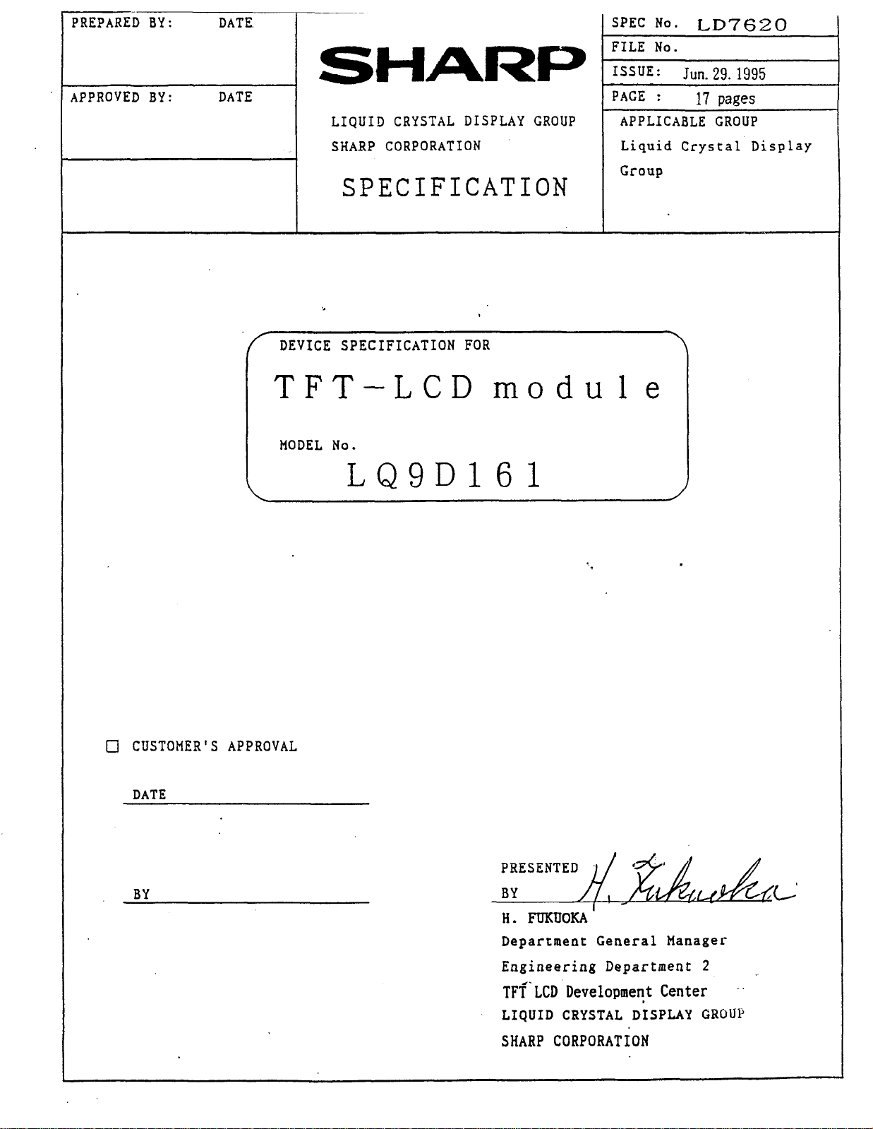
f DEVICE SPECIFICATION FOR
TFT-LCDmodule
MODEL
No.
LQ9D161
ISSUE:
PACE :
APPLICABLE GROUP
Liquid Crystal Display
Group
Jun. 29. 1995
17 Rages
I
0 CUSTOMER’S APPROVAL
DATE
BY
H. FUKIJOKA’
Department General Manager
Engineering Department 2
TFf‘LCD Developmeyt Center ”
LIQUID CRYSTAL DISPLAY GROUP
SHARP CORPORATION
Page 2
RECORDS OF REVISION
Page 3
--. _-- -
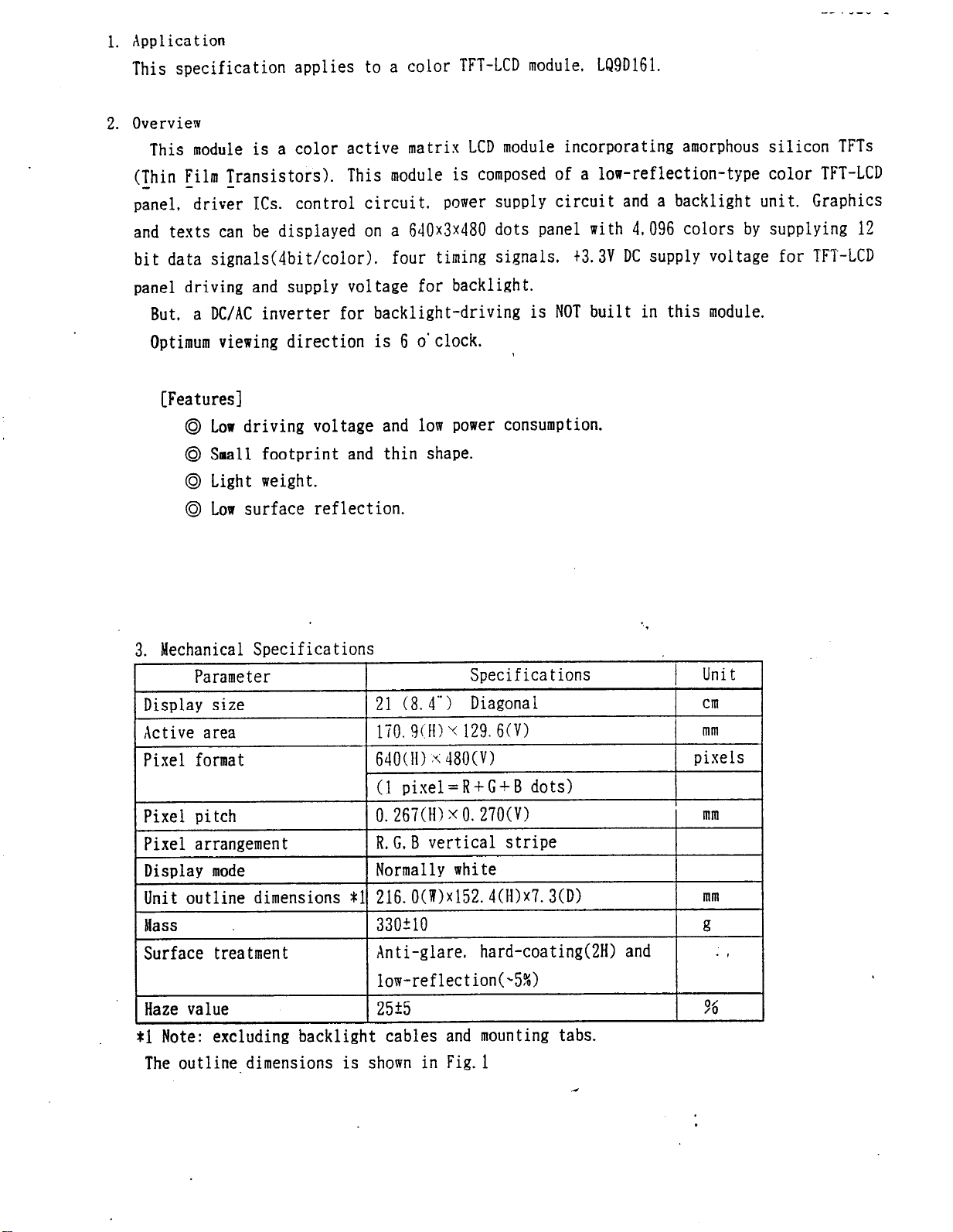
1. Application
This specification appl
ies to a color TFT-LCD module. LQ9D161.
2. Overview
This module is a color active matrix LCD module incorporating amorphous silicon TFTs
(Thin Film Transistors). This module is composed of a low-reflection-type color TFT-LCD
panel, driver ICs. control circuit.
power supply circuit and a backlight unit. Graphics
and texts can be displayed on a 640x3~480 dots panel with 4,096 colors by supplying 12
bit data signals(4bit/color). four timing signals.
t3.3V DC supply voltage for TFT-LCD
panel driving and supply voltage for backlight.
But, a DC/AC inverter for backlight-driving is NOT built in this module.
Optimum viewing direction is 6 o’clock.
[Features]
@ Low driving voltage and low power consumption.
@I Gall footprint and thin shape.
@I Light weight.
@I Low surface reflection.
3. Mechanical Specifications
Parameter
Display size
Active area
21 (8. 4”) Diagonal
170. 9(H) y 129. 6(V)
Specifications
Pixel format 640(H) .u; 480(V)
(1 pixel=R+C+B dots)
Pixel pitch
Pixel arrangement
Display mode
0.267(H) x 0.270(V)
R. G. B vertical stripe
Normally white
Unit outline dimensions *l 216.O(W)x152.4(H)x7.3(D)
Mass 3302 10
Surface treatment
Anti-glare. hard-coating(2H) and
It
Unit
cm
mm
pixels
mm
mm
g
. I
low-reflection(%5%)
Haze value 25+5
tl Note: excluding backlight cables and mounting tabs.
The outline.dimensions is shown in Fig.1
36
Page 4
4. Input Terainals
4-1. TFT-LCD panel driving
The module-side connector:DFSBA-31P-1V (Hirose Electric Co.. Ltd. >
CNl
Pin No.1 Symbolj
1
IRO
GiJD
2
3
Rl
Vsync Vertical synchronous signal
4
5 R2
Hsync Horizontal synchronous signal
6
1
7 1 R3
CND
8
GND
9
10 CK
-11 GO
12
13 Gl
14 TST
15
16
GND
GND
TST ) This should be electrically opened during operatio?
17 G2
18 )
19 t G3
1 20
1 21
TST
1 CPID 1
1 GI’JD
The user-side connector :DFSZ-31S-1V ( n 1, c is blank. A or B.
1 RED data signal (LSB)
RED data signal
RED data signal
1 RED data signal MB)
Clock signal for sampling each data signal
GREEN data signal (LSB)
GREEN data signal
This should be electrically opened during operatinr
/ GREEN data signal
/ This should be electrically opened during ope.ratio{
1 GREEN data signal (NSB)
i
22 1 vcc ( -+ 3.3V
23
I BO
24 -vcc
25
26
27
28
29 B2
30
Bl BLUE data signal
TST This should be electrically opened during operatior
GND
ENAB Signal to settle the horizontal display position
( GND 1
31 lB3
34iThe shielding case is connected with GND in the module.
/ BLUE data signal (LSBI
1 +nv poll& supply
BLUE data signal
) BLUE data signal !KB)
Function 1 Remark ’
I
(Note11
(Note11
I I
/
I I
power supply
[Note21
. ,
. [Note 1 1 One of 480-. 400- and 350-line
mnde is selected depending on
the polari tg combination of the
both synchronous signals.
(Note21 The horizontal display start timing is settled in accord&e with a rising edge of
ENAB signal. Jn case ENAB is fixed “Low”,
‘determined as described in 7-2. Do not keep ENAB “High” during operation.
-
the horizontal
display start timing is
Page 5
4-2. Backlight driving
The module-side connector :BHR-03Wl(JST)
CN2
Pin no. symbol 1
1 V11IGII
3
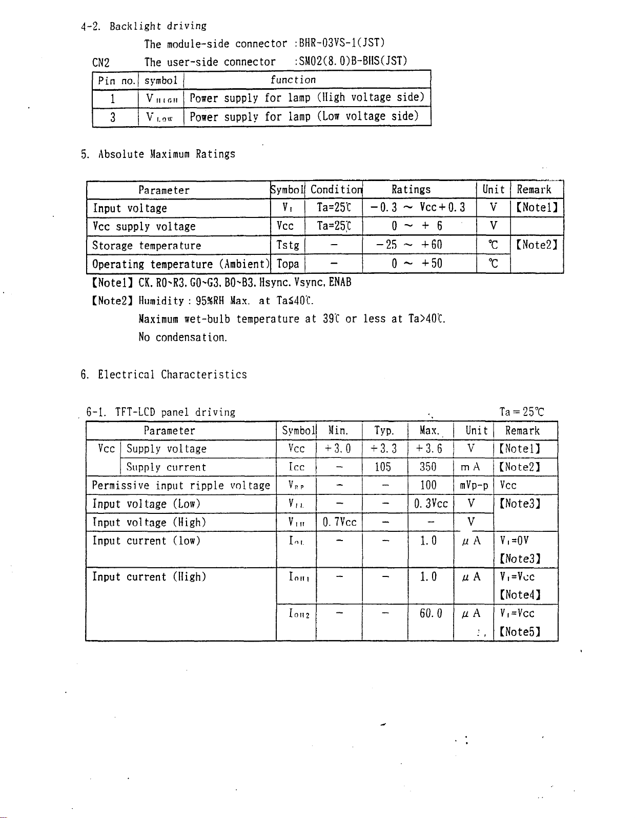
5. Absolute Maximum Ratings
(Note11 CK. ROzR3. GOG3,80~83. Hsync. Vsync, ENAB
(Note‘21 Humidity : 95%RH Max. at Tas4O’C.
The user-side connector
Power supply for lamp (High voltage side)
V C.~K Power supply for lamp (Low voltage side)
Maximum wet-bulb temperature at 39’c or less at Ta>40%.
No condensation.
:SM02(8. O>B-BIIS(JS-0
function
6. Electrical Characteristics
6-l. TFT-LCD panel driving Ta = 25°C
I
Parameter
/ vcc -:iz; 22z -
Permissive input ripple voltage
1 Input voltage (Low)
Input voltage (High)
Input current (low)
Input current (High)
Symbol( hlin.
vcc
ICC -
v
Vr,. - - 0.3vcc v
V
IO,. - - 1. 0
IO,,, / - 1 - / 1.0 / ,u A 1 ;;F=;;,
+3.0 ) +3.3 +3.6 V ) [Notell
RP
,,, 0. 7vcc - - v
1 TYP. 1 Max.. 1
105 350
- -
100
Unit 1 Remark
m A ’ (Note21
mVp-p Vcc
[Note31
fl A
v,=ov
[Note31
Page 6
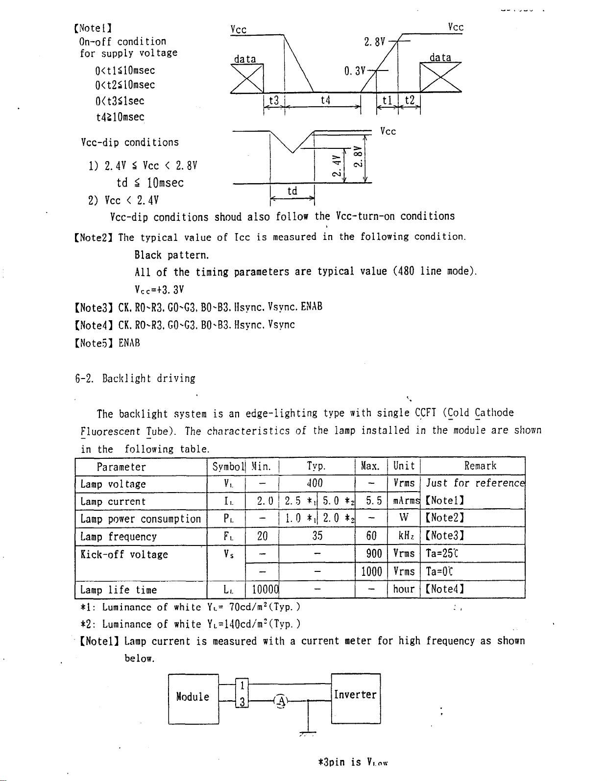
[Note11
I-?
AI”
.
On-off condition
for supply voltage
O<tlSlOmsec
0< t25 1Omsec
O( t3Slsec
t4ZlOmsec
vcc
data
vcc
vcc
Vcc-dip conditions
zz
s’
1) 2.4v S vcc < 2.8V
td 5 1Omsec
2) vcc < 2.4v
Vcc-dip conditions shoud also follow the Vcc-turn-on conditions
(Note21 The typical value of ICC is measured in the following condition.
Black pat tern.
All of the timing parameters are typical value (480 line mode).
vcc=t3.3v
(Note31 CK. RO-R3. GOG3, BO-B3. Hsync. Vsync. ENAB
43
td
-7 &
oi
s 1
(Note41 CK. RO-R3. GO-G3 BO>B3. Hsync. Vsync
(Note51 ENAB
6-2. Bach1 igh t driving
‘.
The backlight system is an edge-lighting type with single CCFT (Gold Cathode
Fluorescent Tube). The characteristics of the lamp installed in the module are shown
in the following table.
-
Lamp life time LI. 1oooc - - hour (Note41
tl: Luminance of white YL= 70cd/m’(Typ.) . I
-
1000 Vrms Ta=OC
*2: Luminance of white Y,.=140cdimz(Typ.)
(Note11 Lamp current is measured with a current meter for high frequency as shown
below.
*3pin is VI.W
Page 7

LD7620-5
(Note21 ralcutated value ior reference.
(IL:<~I.>
(Note31 Lamp frequency may produce interference with horizontal synchronous frequency,
and this may cause beat on the display. Therefore lamp frequency shall be
detached as much as possible from the horizontal synchronous frequency and from
the harmonics of horizontal synchronous to avoid interference.
[Noted] Lamp life time(Ll.) is defined as the time when either 0 or Q) occurs in the
continuous operation under the condition of Ta=25’C and 11.=5.SmArms.
Q Brightness becomes 50% of the original value.
@I Kick-off voltage at Ta=O’C exceeds maximum value. 1000 Vrms.
Note) The performance of the backlight. for example life time or brightness, is much
influenced by the characteristics of the DC-AC inverter for the lamp. lhen you
design or order the inverter. please make sure that a poor lighting caused by the
mismatch of the backlight and the inverter (miss-lighting, flicker, etc.) never
occur. When you confirm it, the module should be operated in the same condition as
it is installed in your instrument.
7. Timing Characteristics of input signals
The timing diagrams of the input signals are shown in Fig.2-Q-0,.
7-l. Timing characteristics
Note) In case of lower frequency, the deterioration of the display. quality, flicker
etc., may be occurred.
Page 8

7-2. Horizontal display position
The horizontal display position is determined by ENAB signal and the input data
corresponding to the rising edge of ENAB signal is displayed at the left end of the
active area.
LD7620-6
Parameter Symbol! Mode ) Min. ) Typ. 1 Max. 1 Unit
ENAB signal Setup time
Pulse width
Hsync-ENAB signal
Tes 1 all 1 s j - Tc-10 ns
Tw ) * 1
Tile ‘I 44 -
2 1 640 640 clock
164
clock
Remark
phase difference
Note) Yhen ENAB is fixed “‘Low”. the display starts from the data of ClO4(clock) as shown
in Fig. 2-Q-Q. Be careful that the module do noJ work when ENAB is fixed “High’.
7-3. Vertical display position
The vertical display position is automatically centered in the active area at each
mode of VGA. 480-, 400- and 350-line mode. Each mode is selected depending on the
polarity of the synchronous signals described in 4-l (Notel).
In each mode, the data of TVn is displayed at the top line of the active area. And
the display position will be centered on the screen like the following figure when the
period of vertical synchronous signal. TV. is typical value.
In 400- and 350-line mode. the data in the vertical data invalid period is also
displayed. So, inputting all data “0” is recommended during vertical data invalid
period.
ENAB signal has no relation to the vertical display position.
mode V-data start(TVs) V-data period(TVd)!/ V-display start(TVn) Unit 1
480 34
480
,
I
34 line
Remark
400 34 400 443-TV line
350 61 350 i 445-TV . line
da ra period
I
data invalid period Miines
NO-line node (TV4491
JODlines
data invalid period : data invalid period :
data period data period 350lines 350lines
data invalid period data invalid period Glines Glines
c 4 c 4
3X-line mode (TV-449
t
631 ines 631 ines
k k
f f
+
Page 9

7-4. Input Data Signals and Display Position on the screen
Display pnsition of input data (W-line
(H-V)
mode)
lDl.DH3t
UP
Dl. DIN30 DMO. DW
I
1 ,
Page 10

Huawr of I Juru
Verrical invalid data period
3.
Tell
tllsrIx9
Eorizoatal
sync. signal
(CL)
Clock signal
llorizontal invalid data period
*IMy .bca EWIIIC Irr~illsl
Data signal
(PO-IKI. CD-C3. uD-u:i)
(ENAU)
Data enable signal
Usync)
sgnc. signal
Vertical
(Bsync)
Borizoatal
sync. signal
Fig.2~(iJ Input signal waveforms (480-line mode)
Data signal
(PD-RX co-CJ. lwU3)
Page 11

d
DKI!) Dfi (I Porizontal invalld ddtrl periad
b
-4 0 1‘3
0 I CD
u lbcr
I
Ferrical invalid ddt;~ period
,I
11
%
.____.__._.--_
.._._..-_....._
TVd
I I I
_ _ . . . . _
U.7)CC
Il. 3bcc
DL! IL1
y Dl
DH3 ' DUI DIP
(400-line mode)
TM
TV
ic Jr,
signal waveforms
m
Fig. 2-Q Input
Tile
$
Tip
Borironral
sync. signal
(llsync)
Clock signal
(a)
Uorizontal invalid data period
Data signal
(PO-iti. CD-C3. BD-BJ)
Data enable signal
(ENAB)
e
il. vcc
Vertical
sync. signal
!
(Vsync)
Horizontal
Vertical jbvalid data period
. .
Data signal
(Rll-RX Glwx. au-sa,
Page 12

DfW 06 B Horizontal invalid data period
u. 3VCC
Verrlcal invalid dara perrod
DHA4!I DIU~D
. . . . ..-v-m..-..
. .._.._______.-
H
Norizonral invalld data period
Tile
Tw
TV
signal waverorms (350-line mode)
Input
_
Tes
?vCC
t,
%
t-
TVP
:-Vertical inralid dara period
!
, Il. 3Ycr
TVh
<
k
Fig. 2-o
signal
liorizontal
sync.
(Usync)
Cl03 signal
ICC)
Data signal
(PB-P3. GO-CJ. MI-US)
Dara enable signal
(ENAB)
Vertical
sync. signal
(Vsync)
Uorizonral
sync. signal
. -
(Bsync)
Dara signal
(R(I-Ii:{. CO-C;I. BD-B3,
Page 13

8. Input Signals. Basic Display Colors and Gray Scale of Each Color
Color & Gray Data signal
scale(GS) GS
RO Rl R2 R3 GO Cl G2 G3 BO Bl I32 83
Black - 0 0 0 0 0 0 0 0 0 0 0 0
Blue - 0 0 0 0 0 0 0 0 1 1 1 1 voltage
Green - 0000
1111 0 0 0 0 1: High leve
0: Low level
Light blue - 0 0 0 O/l 111 1 1 1 1
Red - 111110 0 0 0 0 0 0 0
I 1
Purple - 1 1 1 1 1 IO 0 0 011 11 1
voltage
Brighter GS13 0 0 0 0 0 0 0 0 1 0 1:e 1
0 GS14 0 0 0 0 0 0 0 0 0 1 1 1
Blue GSl5 0 0 0 0 0 0 0 0 1 1 1 1
basic color can be displayed in 16 gray scales from 4 bit data signals.
According to the combination of total 12 bit data signals, the 4.096-colors display
can be achieved on the screen.
*
P
Page 14

9. Optical Characteristics
Ta=25T. Vcc=+3. 3V
late) The measurement shall be executed 30 minutes after lighting at rating.
The optical characteristics shall be measured in a dark room or equivalent state with
the method shown in Fig. 3.
Pho tode tee tor
TFT-LCD module
(BM-5A : TOPCON)
*,
‘..\
1
-3
1: I
LCD panei i
. . . . . . . .._. . . . . . . . . . . . . . ~ ._._........._.__..__-.....-........... _ . . ..- - . . ..-
I
Center of the screen
Fig.3 Optical characteristics measurement method
. . :::
4-
Page 15

[Notell
Definitions
of
viewing angle range:
A-
6 o’clock direction
--*-...
_a-’
Jormal line
9, e’l e21 a12
J$Jj%y
(Note21
(Note31
Definition of contrast,ratio:
The contrast ratio is defined as the foliowing.
Luminance (brightness) of “white”
‘Ontrast Rat1o (CR) = Luminance (brightness) of “black”
Definitions of response time:
The response time is defined as the following figure and shall be measured by
switching the input signal for “black” and
"white".
(Note41
(Note51
This shall be measured at center of the screen.
Definition of white uniformity:
White uniformity is defined as
the following by five-point(AsE)
measurements.
Maximum Luminance of five-point data
bw =
10. Display Quality
Minimum Luminance of five-point data
.d
The display quality of the color TFT-LCD module shall be in compliance with the Incoming
Inspect ion Standard.
Page 16

Handling Precautions
11.
a) Laminated film is attached to the module surface to prevent it from being scratched.
Peel the film off slowly. just before the use. with strict attention to electrostatic
changes. Ionized air shall be blowed over during the action. Blow off ‘dust’ on the
polarizer by using an ionized nitrogen gun. etc.
b) Be sure to turn off the power supply and signal when inserting or disconnecting the
cable.
c) Since LCD panel is made of glass.
Handle with care.
d) The thin liquid crystal layer is packed in the LCD panel. This layer may be disturbed
by the external force when the panel surface is pushed strongly and this disturbance
may cause the transient display non-uniformity. So do not push the panel surface so
strongly.
e) Be sure to design the cabinet so that the module can be instalied without any extra
stress such as warp or twist.
f) Since the front polarizer is easily damaged. pay attention not to scratch it.
it may break or crack if it’s dropped or bumped.
g) lipe off water drop immediately.
or spots.
h) Rhen the panel surface is soiled. wipe it with absorbent cotton or other soft cloth.
i) Since CMOS LSIs are used in this module. take care of static electricity and ensure the
human earth when handling.
j,) Observe all other precautionary requirements in handling co?ponents.
12. Packing form
a) Piling number of cartons : MAX. 7
._
b) Package quantity in one carton : MX. 10
c) Carton size : 374(1)xZ54(HJx314!D)mm
d)Total weight of 1 carton filled with full modules : 4900 g
Packing form is shown in Fig. 4.
Long contact with water may cause discoloration
Page 17

13. Reliability test items
: 58%500ffGravi ty : 9. 8m/s2
Sweep time : 11 minutes
Test period : 3 hours
(non-operating)
[Evaluation Criteria] .
There shall be no change
Display Quality Test conditions.
14. Others
1) Lot
No.
Label:
Direction : CX. +Y. fZ
once for each direction.
which may affect the
(1 hour for each direction of
X, Y, 2
-.
practical use of this display under the
2) Adjusting volume have been set optimally before shipment, so do not change any
adjusted value. If adjusted value is changed. the data mentioned in this technical
literature may not be satisfied.
.3) Disassembling the module can cause permanent damage and should be strictly avoided.
4) Please be careful since image retention may occur when a fixed pattern is displayed
for a long time.
51 If any problem occur in relation to the description of this specifjcation.
it shall be resolved through discussion with spirit of cooperation.
Page 18

electricity
Partition
Fig. 4 Packing form
Page 19

CCFT CONNECTOR NOTES
-2
I
\ -Lz,
I i I
30‘. 1X*,78. 1
BEZEL OPENlHG
I
I
308. ZXI1Z. t
I
-i-- I .i _
I
0
Figl.OUTLlNE DIMENSIONS
I I I
!
f
r-
I
I
r--------------------~----- --_
! I
!
! I
i D
! i ! I I ! I ! i
,
-
-J--.--l----.----------~------------------~-
--t-i
f
0
--
! I
PIN LAYOUT(6Opins)
-
CN~:FXB-~OS-SV(HIR~SE)
INTERFACE CONNECTOR u
Page 20

D
:
]
1
I I
!!. ,
:
!
\,SEE DETAIL B
.__-’
x N .I &&&, .“.,, : &,
vi
4
,’
.- --_-
I
.^ r
_-_-_-_-___ .---- -_ -.-.
R .-- ..- .--. --..--- I j
SECT. C-C SCALE=Z:’
l-n--
Fut I-R
“ETA,L A SCALE=Z:I
NOTES
~14,:0F9--31P-1~ (HIROSE)
CIIZ: BIIR-03VS-1 (JST)
SPACE AROUND CONNECTOI!
ACTIVE AREA
I
1)TOLEAANCE X-DIRECTION A:2. SlfO. 8
2)TOLERANCE X-DIRECTION 8:2. 51fO. E
3)TULERANCE Y-DIRECTION C:Z. 5fO. 8
4)TOLERANCE Y-DIRECTION D:Z. SfO. 6
5)OBLIOUITY OF DISPLAY AREA IE-FI<O. 8
 Loading...