

Page 1
LPC660
Low Power CMOS Quad Operational Amplifier
General Description
The LPC660 CMOS Quad operational amplifier is ideal for
operation from a single supply. It features a wide range of
operating voltages from +5V to +15V and features rail-to-rail
output swing in addition to an input common-mode range
that includes ground. Performance limitations that have
plagued CMOS amplifiers in the past are not a problem with
this design. Input V
OS
, drift, and broadband noise as well as
voltage gain (into 100 kΩ and5kΩ) are all equal to or better
than widely accepted bipolar equivalents, while the power
supply requirement is typically less than 1 mW.
This chip is built with National’s advanced Double-Poly
Silicon-Gate CMOS process.
See the LPC662 datasheet for a Dual CMOS operational
amplifier and LPC661 datasheet for a single CMOS operational amplifier with these same features.
Applications
n High-impedance buffer
n Precision current-to-voltage converter
n Long-term integrator
n High-impedance preamplifier
n Active filter
n Sample-and-Hold circuit
n Peak detector
Features
n Rail-to-rail output swing
n Micropower operation: (1 mW)
n Specified for 100 kΩ and5kΩloads
n High voltage gain: 120 dB
n Low input offset voltage: 3 mV
n Low offset voltage drift: 1.3 µV/˚C
n Ultra low input bias current: 2 fA
n Input common-mode includes V
−
n Operation range from +5V to +15V
n Low distortion: 0.01%at 1 kHz
n Slew rate: 0.11 V/µs
n Full military temp. range available
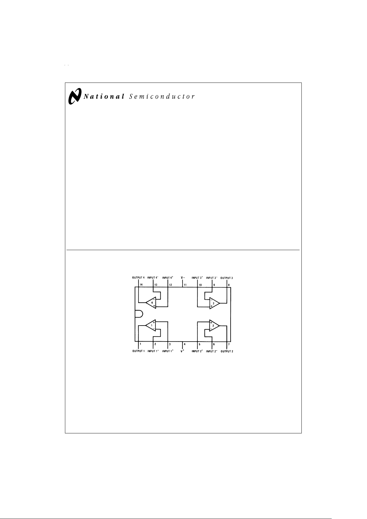
Connection Diagram
14-Pin DIP/SO
DS010547-1
Top View
March 1998
LPC660 Low Power CMOS Quad Operational Amplifier
© 1999 National Semiconductor Corporation DS010547 www.national.com
Page 2
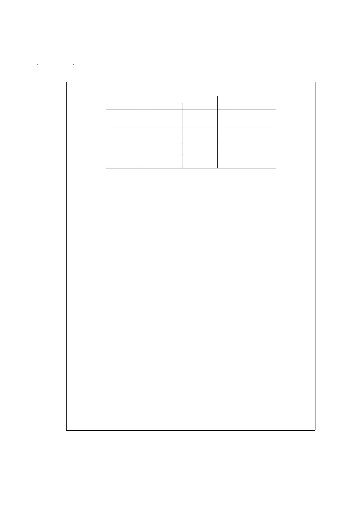
Ordering Information
Package Temperature Range NSC
Drawing
Transport
Media
Military Industrial
14-Pin LPC660AMD D14E Rail
Side Brazed
Ceramic DIP
14-Pin LPC660AIM M14A Rail
Small Outline or LPC660IM Tape and Reel
14-Pin LPC660AIN N14A Rail
Molded DIP or LPC660IN
14-Pin LPC660AMJ/883 J14A Rail
Ceramic DIP
www.national.com 2
Page 3
Absolute Maximum Ratings (Note 3)
If Military/Aerospace specified devices are required,
please contact theNational Semiconductor Sales Office/
Distributors for availability and specifications.
Differential Input Voltage
±
Supply Voltage
Supply Voltage (V
+−V−
) 16V
Output Short Circuit to V
+
(Note 11)
Output Short Circuit to V
−
(Note 1)
Lead Temperature
(Soldering, 10 sec.) 260˚C
Storage Temp. Range −65˚C to +150˚C
Junction Temperature (Note 2) 150˚C
ESD Rating
(C=100 pF, R=1.5 kΩ) 1000V
Power Dissipation (Note 2)
Current at Input Pin
±
5mA
Current at Output Pin
±
18 mA
Voltage at Input/Output Pin (V
+
) + 0.3V, (V−) − 0.3V
Current at Power Supply Pin 35 mA
Operating Ratings (Note 3)
Temperature Range
LPC660AM −55˚C ≤ T
J
≤ +125˚C
LPC660AI −40˚C ≤ T
J
≤ +85˚C
LPC660I −40˚C ≤ T
J
≤ +85˚C
Supply Range 4.75V to 15.5V
Power Dissipation (Note 9)
Thermal Resistance (θ
JA
), (Note 10)
14-Pin Ceramic DIP 90˚C/W
14-Pin Molded DIP 85˚C/W
14-Pin SO 115˚C/W
14-Pin Side Brazed Ceramic DIP 90˚C/W
DC Electrical Characteristics
Unless otherwise specified, all limits guaranteed for T
J
=
25˚C. Boldface limits apply at the temperature extremes. V
+
=
5V, V
−
=
0V, V
CM
=
1.5V, V
O
=
2.5V, and R
L
>
1M unless otherwise specified.
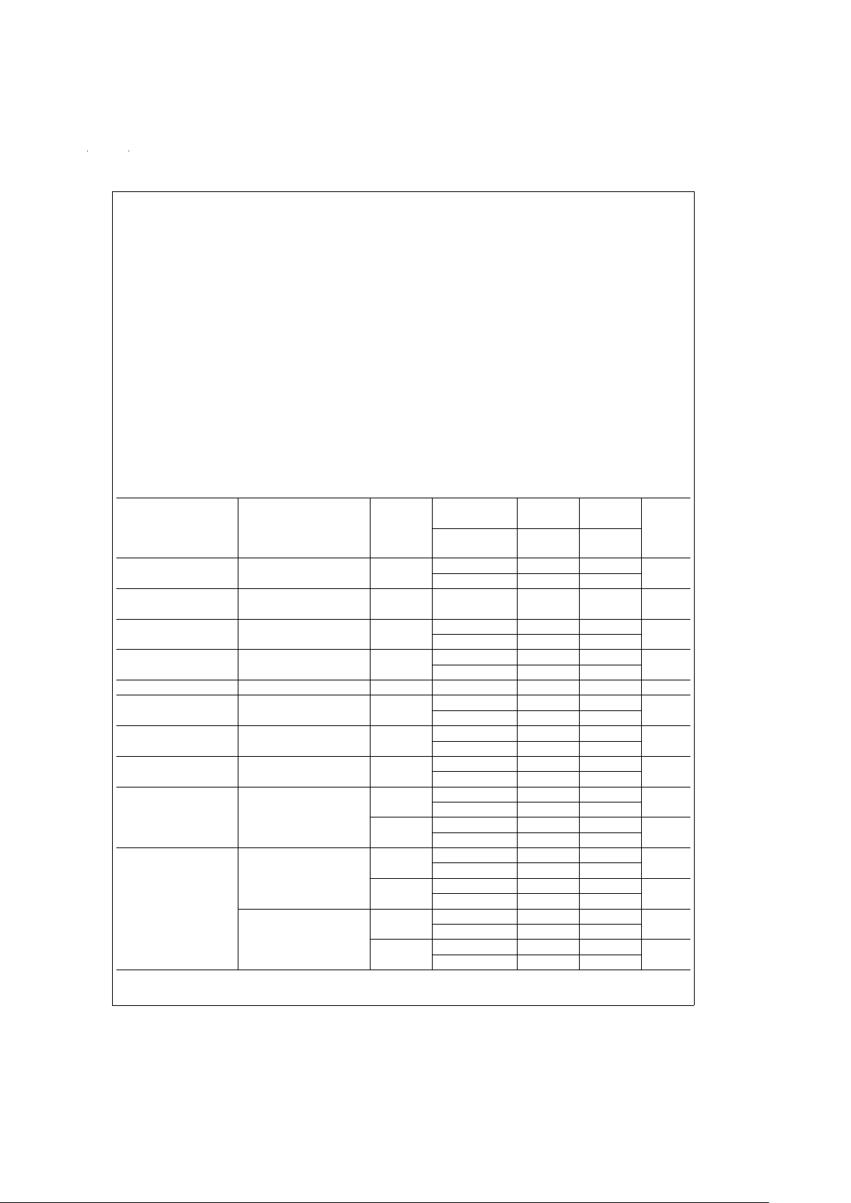
Parameter Conditions Typ LPC660AM LPC660AI LPC660I Units
LPC660AMJ/883
Limit Limit Limit
(Notes 4, 8) (Note 4) (Note 4)
Input Offset Voltage 1 3 3 6 mV
3.5 3.3 6.3 max
Input Offset Voltage 1.3 µV/˚C
Average Drift
Input Bias Current 0.002 20 pA
100 4 4 max
Input Offset Current 0.001 20 pA
100 2 2 max
Input Resistance
>
1 Tera Ω
Common Mode 0V ≤ V
CM
≤ 12.0V 83 70 70 63 dB
Rejection Ratio V
+
=
15V 68 68 61 min
Positive Power Supply 5V ≤ V
+
≤ 15V 83 70 70 63 dB
Rejection Ratio 68 68 61 min
Negative Power Supply 0V ≤ V
−
≤ −10V 94 84 84 74 dB
Rejection Ratio 82 83 73 min
Input Common Mode V
+
=
5V & 15V −0.4 −0.1 −0.1 −0.1 V
Voltage Range For CMRR
>
50 dB 000max
V
+
− 1.9 V+− 2.3 V+− 2.3 V+− 2.3 V
V
+
− 2.6 V+− 2.5 V+− 2.5 min
Large Signal R
L
=
100 kΩ (Note 5) 1000 400 400 300 V/mV
Voltage Gain Sourcing 250 300 200 min
Sinking 500 180 180 90 V/mV
70 120 70 min
R
L
=
5kΩ(Note 5) 1000 200 200 100 V/mV
Sourcing 150 160 80 min
Sinking 250 100 100 50 V/mV
35 60 40 min
www.national.com3
Page 4
DC Electrical Characteristics (Continued)
Unless otherwise specified, all limits guaranteed for T
J
=
25˚C. Boldface limits apply at the temperature extremes. V
+
=
5V, V
−
=
0V, V
CM
=
1.5V, V
O
=
2.5V, and R
L
>
1M unless otherwise specified.
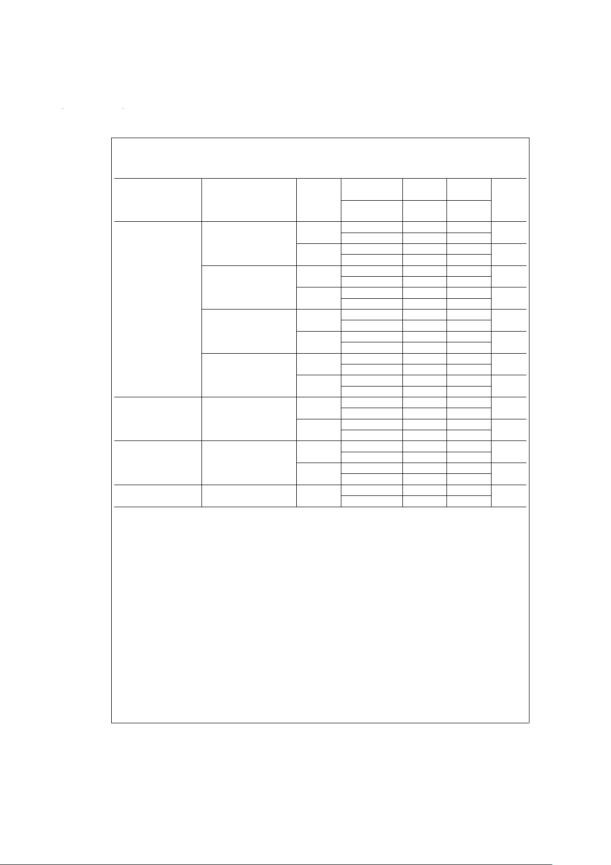
Parameter Conditions Typ LPC660AM LPC660AI LPC660I Units
LPC660AMJ/883
Limit Limit Limit
(Notes 4, 8) (Note 4) (Note 4)
Output Swing V
+
=
5V 4.987 4.970 4.970 4.940 V
R
L
=
100 kΩ to V
+
/2 4.950 4.950 4.910 min
0.004 0.030 0.030 0.060 V
0.050 0.050 0.090 max
V
+
=
5V 4.940 4.850 4.850 4.750 V
R
L
=
5kΩto V
+
/2 4.750 4.750 4.650 min
0.040 0.150 0.150 0.250 V
0.250 0.250 0.350 max
V
+
=
15V 14.970 14.920 14.920 14.880 V
R
L
=
100 kΩ to V
+
/2 14.880 14.880 14.820 min
0.007 0.030 0.030 0.060 V
0.050 0.050 0.090 max
V
+
=
15V 14.840 14.680 14.680 14.580 V
R
L
=
5kΩto V
+
/2 14.600 14.600 14.480 min
0.110 0.220 0.220 0.320 V
0.300 0.300 0.400 max
Output Current Sourcing, V
O
=
0V 22 16 16 13 mA
V
+
=
5V 12 14 11 min
Sinking, V
O
=
5V 21 16 16 13 mA
12 14 11 min
Output Current Sourcing, V
O
=
0V 40 19 28 23 mA
V
+
=
15V 19 25 20 min
Sinking, V
O
=
13V 39 19 28 23 mA
(Note 11) 19 24 19 min
Supply Current All Four Amplifiers 160 200 200 240 µA
V
O
=
1.5V 250 230 270 max
www.national.com 4
Page 5
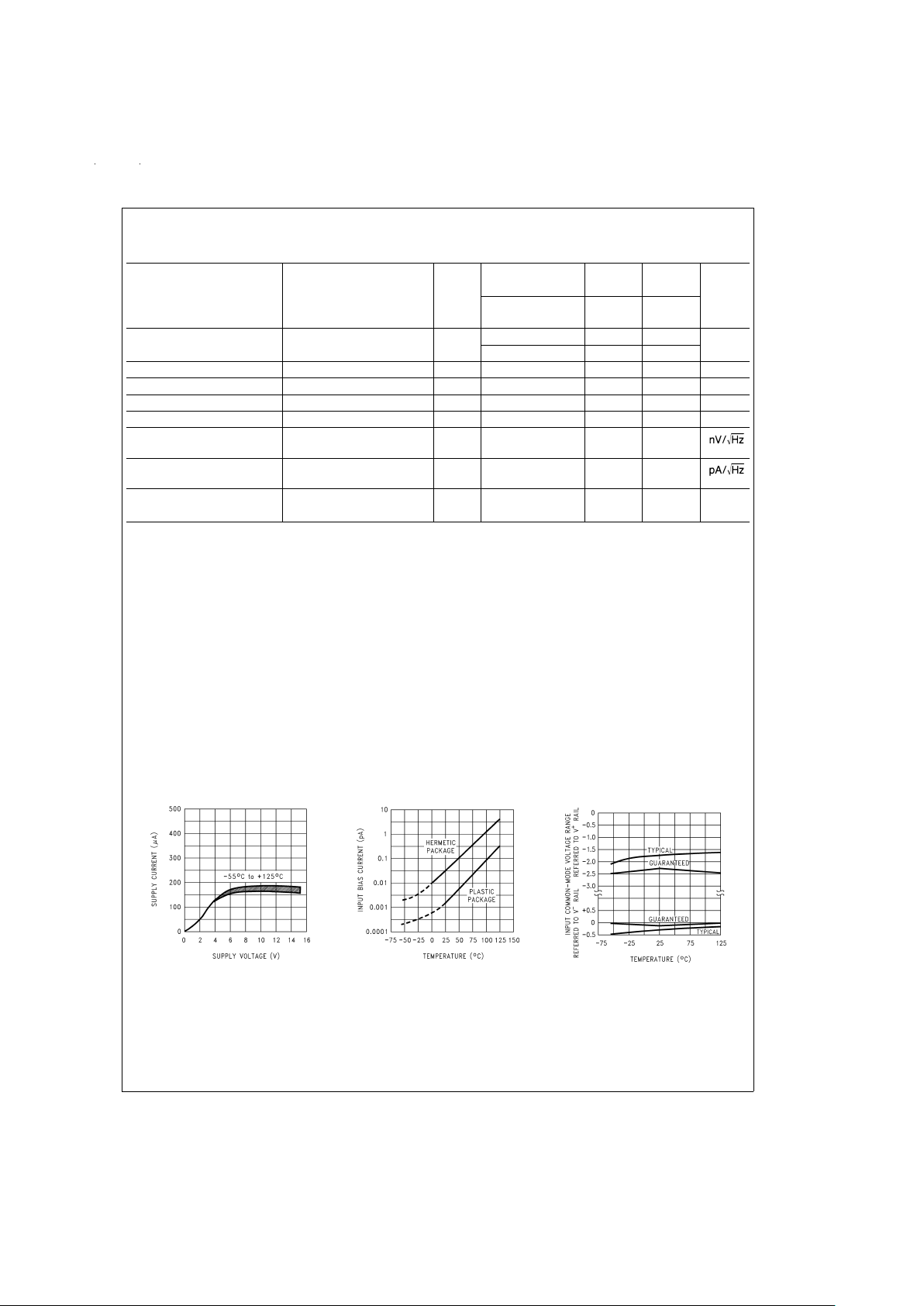
AC Electrical Characteristics
Unless otherwise specified, all limits guaranteed for T
J
=
25˚C. Boldface limits apply at the temperature extremes. V
+
=
5V, V
−
=
0V, V
CM
=
1.5V, V
O
=
2.5, and R
L
>
1M unless otherwise specified.
Parameter Conditions Typ LPC660AM LPC660AI LPC660I Units
LPC660AMJ/883
Limit Limit Limit
(Notes 4, 8) (Note 4) (Note 4)
Slew Rate (Note 6) 0.11 0.07 0.07 0.05 V/µs
0.04 0.05 0.03 min
Gain-Bandwidth Product 0.35 MHz
Phase Margin 50 Deg
Gain Margin 17 dB
Amp-to-Amp Isolation (Note 7) 130 dB
Input Referred Voltage Noise F=1 kHz 42
Input Referred Current Noise F=1 kHz 0.0002
Total Harmonic Distortion F=1 kHz, A
V
=
−10 0.01
%
R
L
=
100 kΩ,V
O
=
8V
PP
Note 1: Applies to both single supply and split supply operation. Continuous short circuit operation at elevated ambient temperature and/or multiple Op Amp shorts
can result in exceeding the maximum allowed junction temperature of 150˚C. Output currents in excess of
±
30 mA over long term may adversely affect reliability.
Note 2: The maximum power dissipation is a function of T
J(max)
, θJAand TA. The maximum allowable power dissipation at any ambient temperature is P
D
=
(T
J(max)–TA)θJA
.
Note 3: Absolute Maximum Ratings indicate limits beyond which damage to the device may occur. Operating Ratings indicate conditions for which the device is intended to be functional, but do not guarantee specific performance limits. For guaranteed specifications and test conditions, see the Electrical Characteristics. The
guaranteed specifications apply only for the test conditions listed.
Note 4: Limits are guaranteed by testing or correlation.
Note 5: V
+
=
15V, V
CM
=
7.5V and R
L
connected to 7.5V. For Sourcing tests, 7.5V ≤ VO≤ 11.5V. For Sinking tests, 2.5V ≤ VO≤ 7.5V.
Note 6: V
+
=
15V. Connected as Voltage Follower with 10V step input. Number specified is the slower of the positive and negative slew rates.
Note 7: Input referred. V
+
=
15V and R
L
=
100 kΩ connected to V
+
/2. Each amp excited in turn with 1 kHz to produce V
O
=
13 V
PP
.
Note 8: Amilitary RETS electrical test specification is available on request. At the time of printing, the LPC660AMJ/883 RETS specification complied fully with the
boldface limits in this column. The LPC660AMJ/883 may also be procured to a Standard Military Drawing specification.
Note 9: For operating at elevated temperatures, the device must be derated based on the thermal resistance θ
JA
with P
D
=
(T
J–TA
)/θJA.
Note 10: All numbers apply for packages soldered directly into a PC board.
Note 11: Do not connect output to V
+
when V+is greater than 13V or reliability may be adversely affected.
Typical Performance Characteristics V
S
=
±
7.5V, T
A
=
25˚C unless otherwise specified
Supply Current
vs Supply Voltage
DS010547-27
Input Bias Current
vs Temperature
DS010547-28
Common-Mode Voltage
Range vs Temperature
DS010547-29
www.national.com5
Page 6
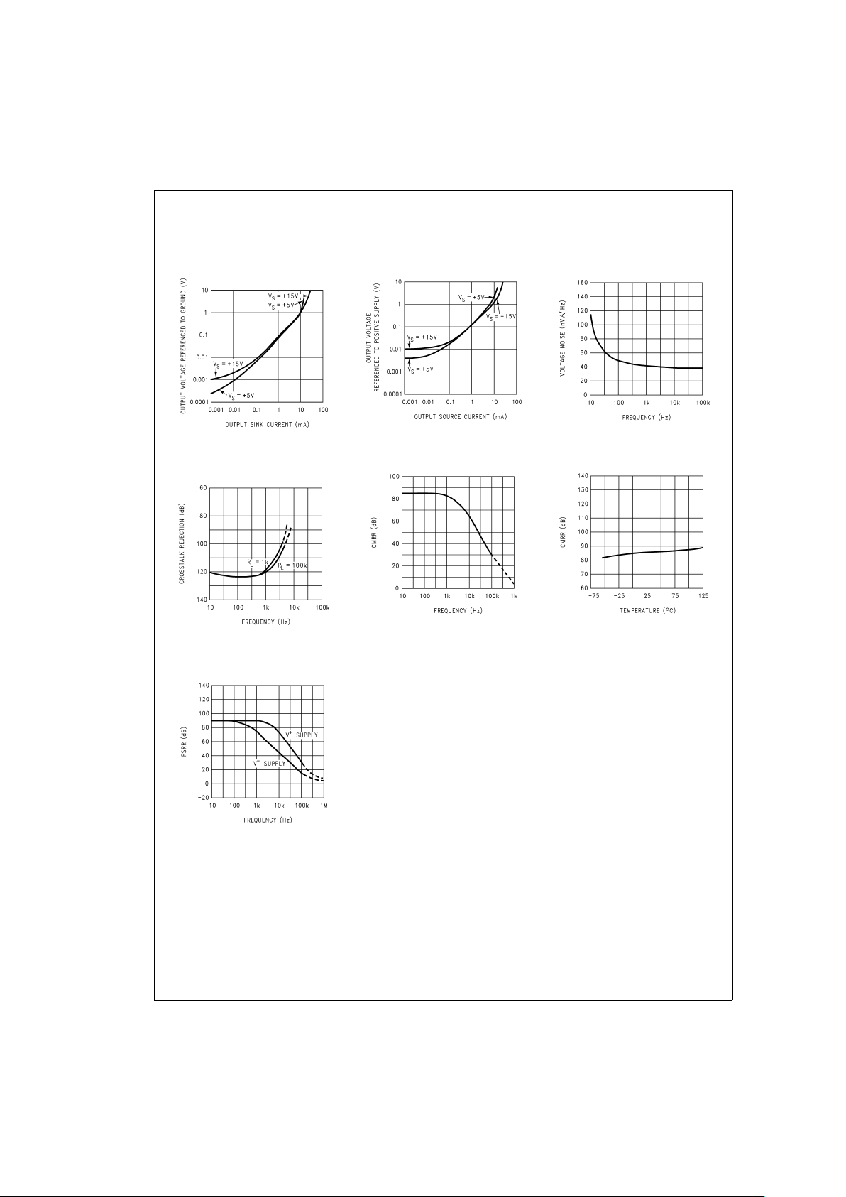
Typical Performance Characteristics V
S
=
±
7.5V, T
A
=
25˚C unless otherwise
specified (Continued)
Output Characteristics
Current Sinking
DS010547-30
Output Characteristics
Current Sourcing
DS010547-31
Input Voltage Noise
vs Frequency
DS010547-32
Crosstalk Rejection
vs Frequency
DS010547-33
CMRR vs Frequency
DS010547-34
CMRR vs Temperature
DS010547-35
Power Supply Rejection
Ratio vs Frequency
DS010547-36
www.national.com 6
Page 7
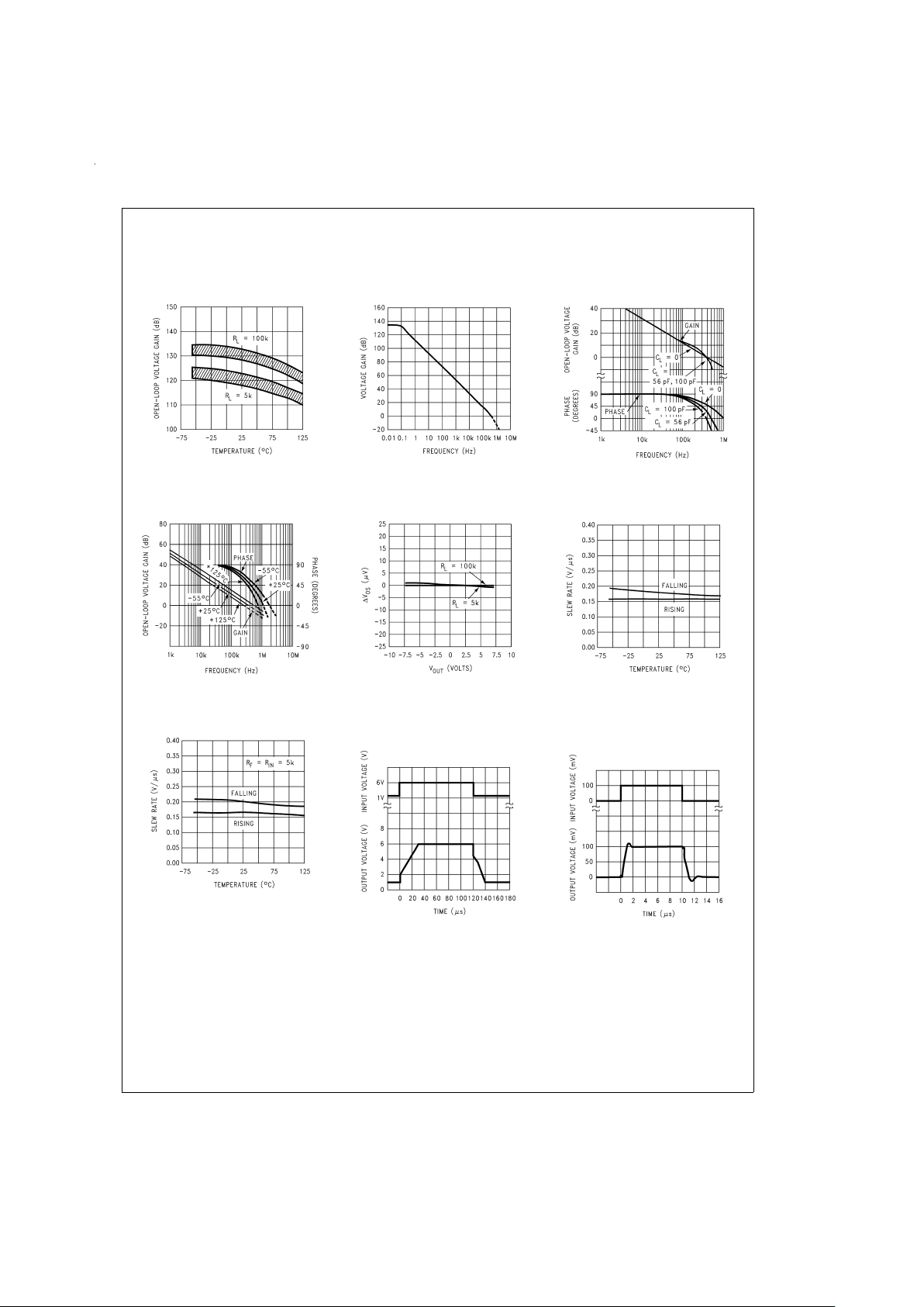
Typical Performance Characteristics V
S
=
±
7.5V, T
A
=
25˚C unless otherwise
specified (Continued)
Open-Loop Voltage Gain
vs Temperature
DS010547-37
Open-Loop
Frequency Response
DS010547-38
Gain and Phase Responses
vs Load Capacitance
DS010547-39
Gain and Phase Responses
vs Temperature
DS010547-40
Gain Error
(V
OS
vs V
OUT
)
DS010547-41
Non-Inverting Slew Rate
vs Temperature
DS010547-42
Inverting Slew Rate
vs Temperature
DS010547-43
Large-Signal Pulse
Non-Inverting Response
(A
V
=
+1)
DS010547-44
Non-Inverting Small
Signal Pulse Response
(A
V
=
+1)
DS010547-45
www.national.com7
Page 8
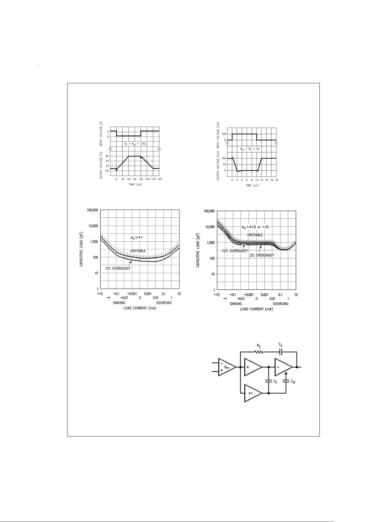
Typical Performance Characteristics V
S
=
±
7.5V, T
A
=
25˚C unless otherwise
specified (Continued)
Application Hints
AMPLIFIER TOPOLOGY
The topology chosen for the LPC660 is unconventional
(compared to general-purpose op amps) in that the traditional unity-gain buffer output stage is not used; instead, the
output is taken directly from the output of the integrator,to allow rail-to-rail output swing. Since the buffer traditionally delivers the power to the load, while maintaining high op amp
gain and stability, and must withstand shorts to either rail,
these tasks now fall to the integrator.
As a result of these demands, the integrator is a compound
affair with an embedded gain stage that is doubly fed forward
(via C
f
and Cff) by a dedicated unity-gain compensation
driver. In addition, the output portion of the integrator is a
push-pull configuration for delivering heavy loads. While
sinking current the whole amplifier path consists of three
gain stages with one stage fed forward, whereas while
sourcing the path contains four gain stages with two fed
forward.
The large signal voltage gain while sourcing is comparable
to traditional bipolar op amps, for load resistance of at least
5kΩ. The gain while sinking is higher than most CMOS op
Inverting Large-Signal
Pulse Response
DS010547-46
Inverting Small-Signal
Pulse Response
DS010547-47
Stability vs Capacitive Load
DS010547-4
Note: Avoid resistive loads of less than 500Ω, as they may cause
instability.
Stability vs Capacitive Load
DS010547-5
DS010547-6
FIGURE 1. LPC660 Circuit Topology (Each Amplifier)
www.national.com 8
Page 9
Application Hints (Continued)
amps, due to the additional gain stage; however, when driving load resistance of 5 kΩ or less, the gain will be reduced
as indicated in the Electrical Characteristics. The op amp
can drive load resistance as low as 500Ω without instability.
COMPENSATING INPUT CAPACITANCE
Refer to the LMC660 or LMC662 datasheets to determine
whether or not a feedback capacitor will be necessary for
compensation and what the value of that capacitor would be.
CAPACITIVE LOAD TOLERANCE
Like many other op amps, the LPC660 may oscillate when
its applied load appears capacitive. The threshold of oscillation varies both with load and circuit gain. The configuration
most sensitive to oscillation is a unity-gain follower. See the
Typical Performance Characteristics.
The load capacitance interacts with the op amp’s output resistance to create an additional pole. If this pole frequency is
sufficiently low, it will degrade the op amp’s phase margin so
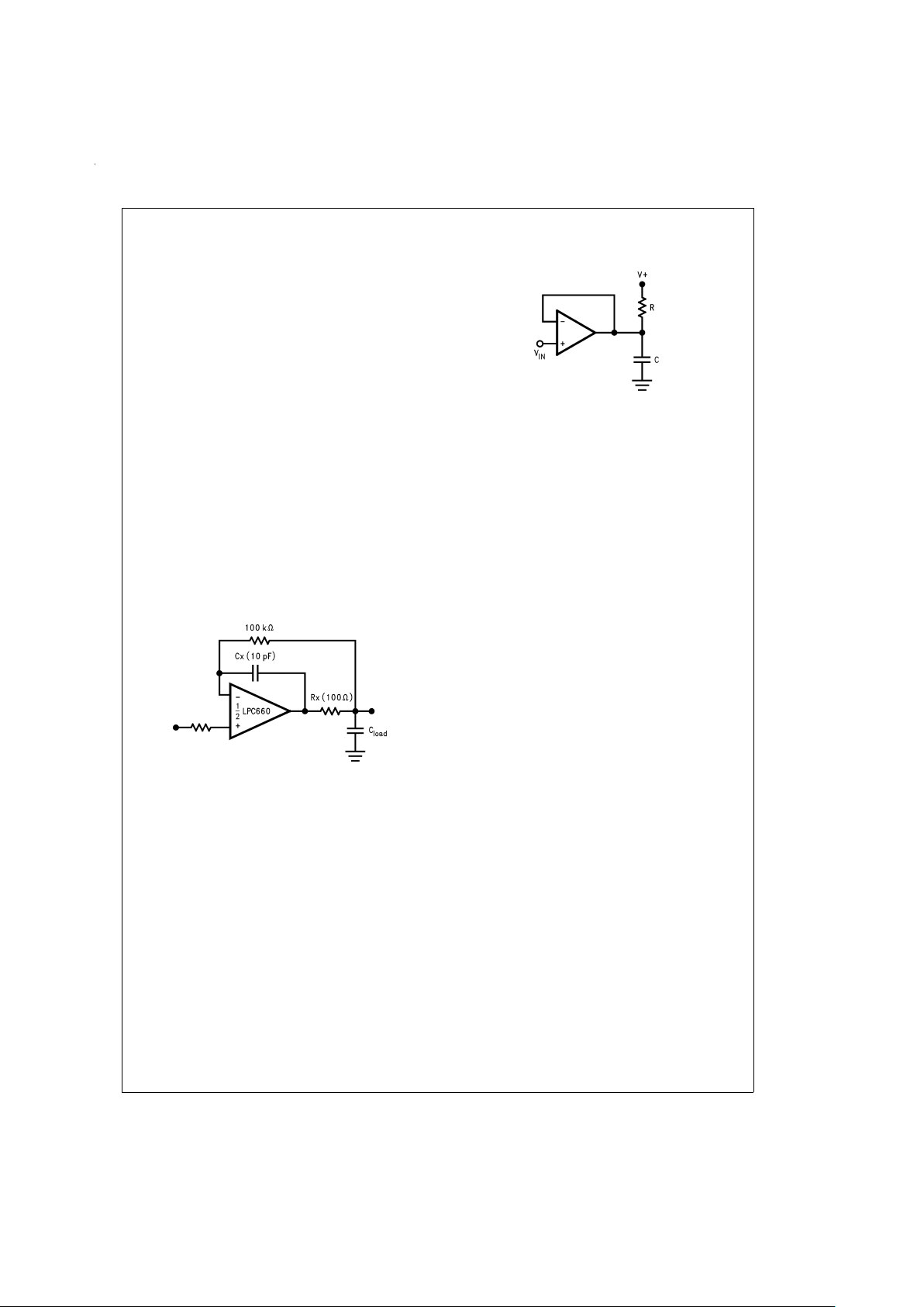
that the amplifier is no longer stable at low gains. The addition of a small resistor (50Ω to 100Ω) in series with the op
amp’s output, and a capacitor (5 pF to 10 pF) from inverting
input to output pins, returns the phase margin to a safe value
without interfering with lower-frequency circuit operation.
Thus, larger values of capacitance can be tolerated without
oscillation. Note that in all cases, the output will ring heavily
when the load capacitance is near the threshold for
oscillation.
Capacitive load driving capability is enhanced by using a pull
up resistor to V
+
(
Figure 3
). Typically a pull up resistor conducting 50 µA or more will significantly improve capacitive
load responses. The value of the pull up resistor must be determined based on the current sinking capability of the ampli-
fier with respect to the desired output swing. Open loop gain
of the amplifier can also be affected by the pull up resistor
(see Electrical Characteristics).
PRINTED-CIRCUIT-BOARD LAYOUT
FOR HIGH-IMPEDANCE WORK
It is generally recognized that any circuit which must operate
with less than 1000 pA of leakage current requires special
layout of the PC board. When one wishes to take advantage
of the ultra-low bias current of the LPC660, typically less
than 0.04 pA, it is essential to have an excellent layout. Fortunately, the techniques for obtaining low leakages are quite
simple. First, the user must not ignore the surface leakage of
the PC board, even though it may sometimes appear acceptably low, because under conditions of high humidity or dust
or contamination, the surface leakage will be appreciable.
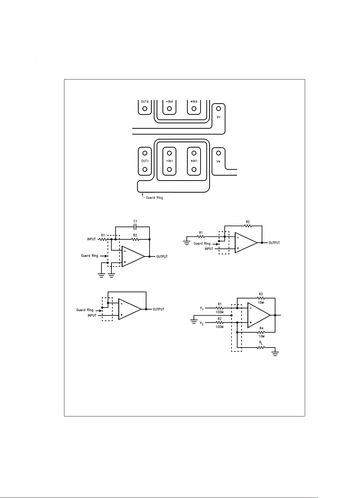
To minimize the effect of any surface leakage, lay out a ring
of foil completely surrounding the LPC660’s inputs and the
terminals of capacitors, diodes, conductors, resistors, relay
terminals, etc. connected to the op-amp’s inputs. See
Figure
4
. To have a significant effect, guard rings should be placed
on both the top and bottom of the PC board. This PC foil
must then be connected to a voltage which is at the same
voltage as the amplifier inputs, since no leakage current can
flow between two points at the same potential. For example,
a PC board trace-to-pad resistance of 10
12
ohms, which is
normally considered a very large resistance, could leak 5 pA
if the trace were a 5V bus adjacent to the pad of an input.
This would cause a 100 times degradation from the
LPC660’s actual performance. However, if a guard ring is
held within 5 mV of the inputs, then even a resistance of
10
11
ohms would cause only 0.05 pA of leakage current, or
perhaps a minor (2:1) degradation of the amplifier’s performance. See
Figure 5a,Figure 5b,Figure 5c
for typical connections of guard rings for standard op-amp configurations.
If both inputs are active and at high impedance, the guard
can be tied to ground and still provide some protection; see
Figure 5d
.
DS010547-7
FIGURE 2. Rx, Cx Improve Capacitive Load Tolerance
DS010547-26
FIGURE 3. Compensating for Large
Capacitive Loads with A Pull Up Resistor
www.national.com9
Page 10
Application Hints (Continued)
The designer should be aware that when it is inappropriate
to lay out a PC board for the sake of just a few circuits, there
is another technique which is even better than a guard ring
on a PC board: Don’t insert the amplifier’s input pin into the
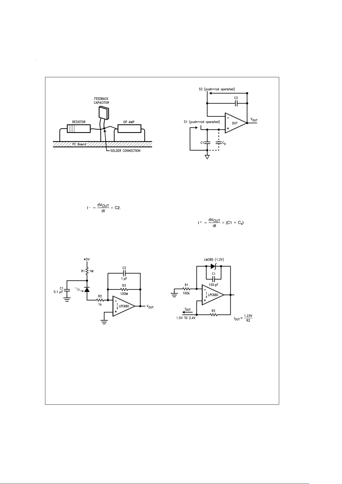
board at all, but bend it up in the air and use only air as an insulator. Air is an excellent insulator. In this case you may
have to forego some of the advantages of PC board con-
struction, but the advantages are sometimes well worth the
effort of using point-to-point up-in-the-air wiring.
See
Figure 6
.
DS010547-19
FIGURE 4. Example of Guard Ring in P.C. Board Layout using the LPC660
DS010547-20
(a) Inverting Amplifier
DS010547-21
(b) Non-Inverting Amplifier
DS010547-22
(c) Follower
DS010547-23
(d) Howland Current Pump
FIGURE 5. Guard Ring Connections
www.national.com 10
Page 11
Application Hints (Continued)
BIAS CURRENT TESTING
The test method of
Figure 7
is appropriate for bench-testing
bias current with reasonable accuracy.To understand its operation, first close switch S2 momentarily. When S2 is
opened, then
A suitable capacitor for C2 would be a 5 pF or 10 pF silver
mica, NPO ceramic, or air-dielectric. When determining the
magnitude of I
−
, the leakage of the capacitor and socket
must be taken into account. Switch S2 should be left shorted
most of the time, or else the dielectric absorption of the capacitor C2 could cause errors.
Similarly, if S1 is shorted momentarily (while leaving S2
shorted)
where Cxis the stray capacitance at the + input.
Typical Single-Supply Applications (V
+
=
5.0 V
DC
)
DS010547-24
(Input pins are lifted out of PC board and soldered directly to components.
All other pins connected to PC board.)
FIGURE 6. Air Wiring
DS010547-25
FIGURE 7. Simple Input Bias Current Test Circuit
Photodiode Current-to-Voltage Converter
DS010547-17
Note: A 5V bias on the photodiode can cut its capacitance by a factor of 2
or 3, leading to improved response and lower noise. However, this bias on
the photodiode will cause photodiode leakage (also known as its dark
current).
Micropower Current Source
DS010547-18
Note: (Upper limit of output range dictated by input common-mode range;
lower limit dictated by minimum current requirement of LM385.)
www.national.com11
Page 12
Typical Single-Supply Applications (V
+
=
5.0 V
DC
) (Continued)
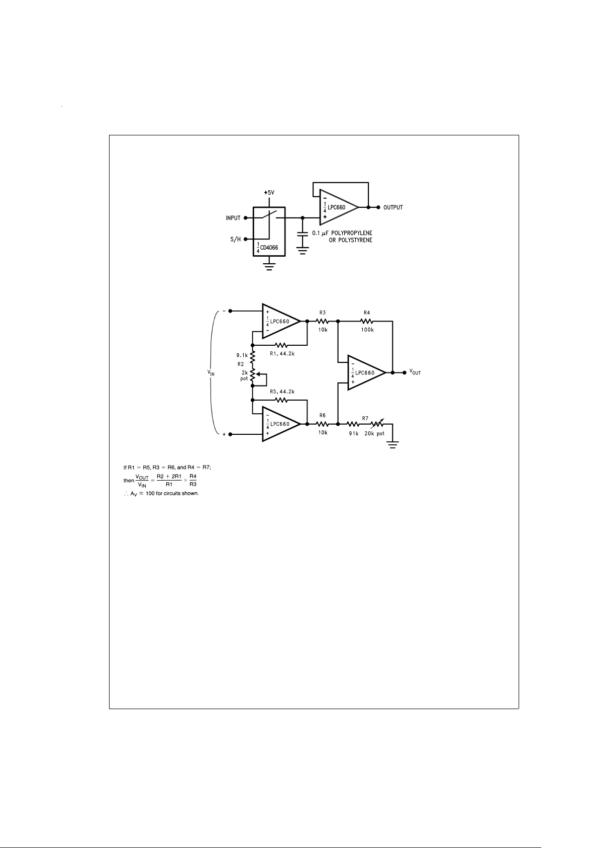
Low-Leakage Sample-and-Hold
DS010547-8
Instrumentation Amplifier
DS010547-9
For good CMRR over temperature, low drift resistors should be used. Matching of R3 to R6 and R4 to R7 affects CMRR. Gain may be adjusted through R2.
CMRR may be adjusted through R7.
www.national.com 12
Page 13
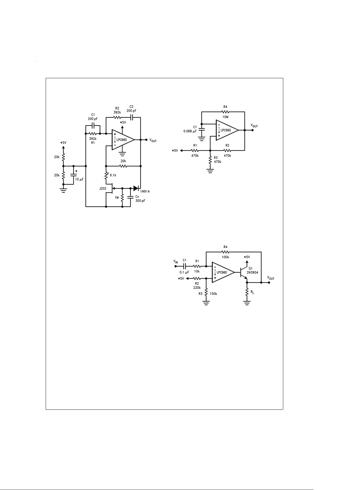
Typical Single-Supply Applications (V
+
=
5.0 V
DC
) (Continued)
This circuit, as shown, oscillates at 2.0 kHz with a
peak-to-peak output swing of 4.5V
Sine-Wave Oscillator
DS010547-10
Oscillator frequency is determined by R1, R2, C1, and C2:
f
OSC
=
1/2πRC
where R=R1=R2 and C=C1=C2.
1 Hz Square-Wave Oscillator
DS010547-11
Power Amplifier
DS010547-12
www.national.com13
Page 14
Typical Single-Supply Applications (V
+
=
5.0 V
DC
) (Continued)
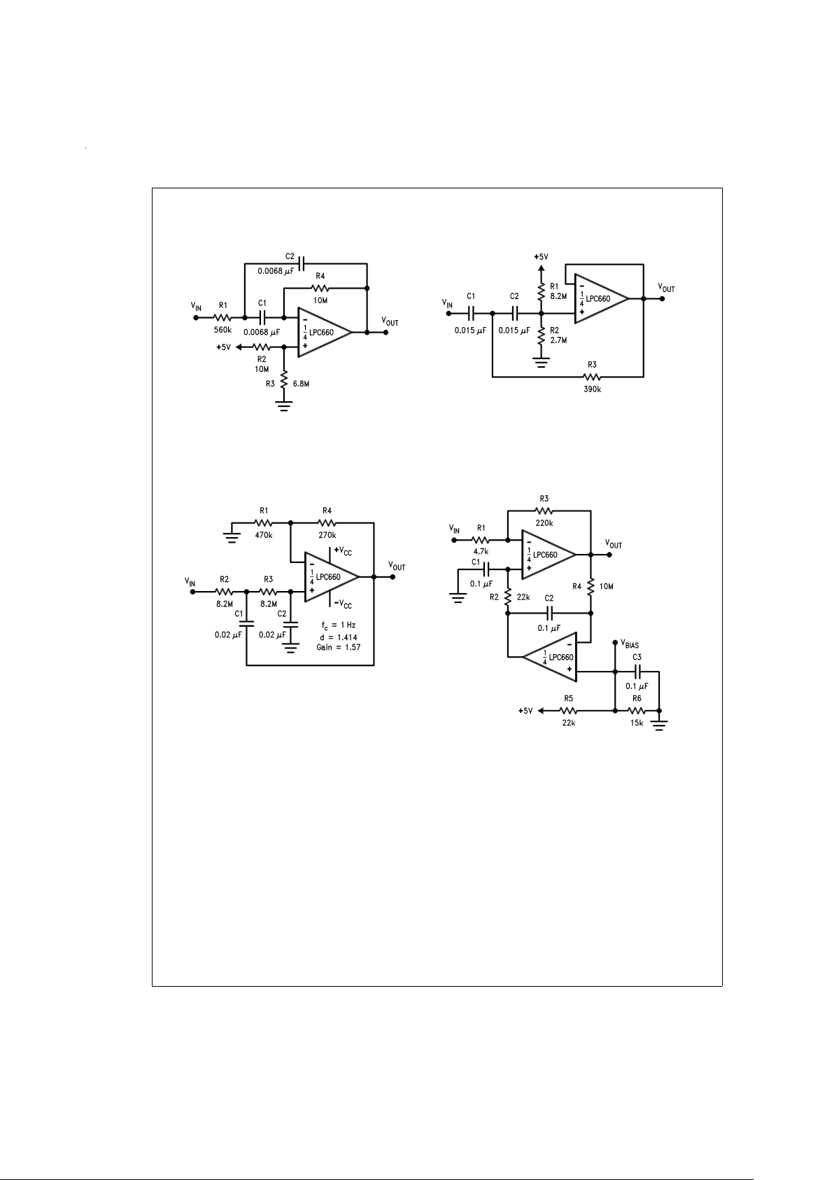
10 Hz Bandpass Filter
DS010547-13
f
O
=
10 Hz
Q=2.1
Gain=−8.8
10 Hz High-Pass Filter (2 dB Dip)
DS010547-14
f
c
=
10 Hz
d=0.895
Gain=1
1 Hz Low-Pass Filter
(Maximally Flat, Dual Supply Only)
DS010547-15
High Gain Amplifier with Offset Voltage Reduction
DS010547-16
Gain=−46.8
Output offset voltage reduced to the level of the input offset voltage of the
bottom amplifier (typically 1 mV), referred to V
BIAS
.
www.national.com 14
Page 15
Physical Dimensions inches (millimeters) unless otherwise noted
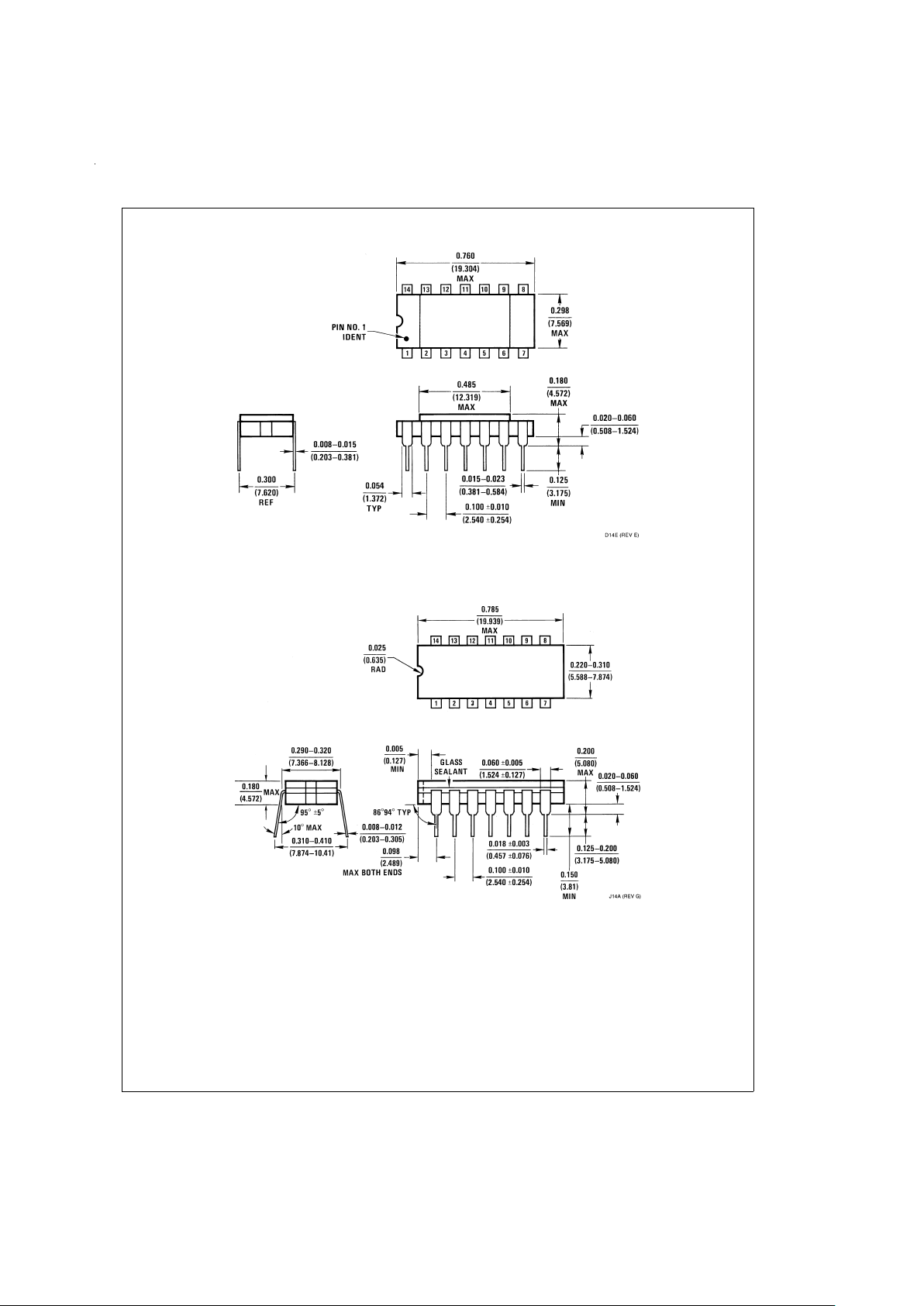
14-Pin Cavity Dual-In-Line Package (D)
Order Number LPC660AMD
NS Package Number D14E
14-Lead Ceramic Dual-In-Line Package (J)
Order Number LPC660AMJ/883
NS Package Number J14A
www.national.com15
Page 16
Physical Dimensions inches (millimeters) unless otherwise noted (Continued)
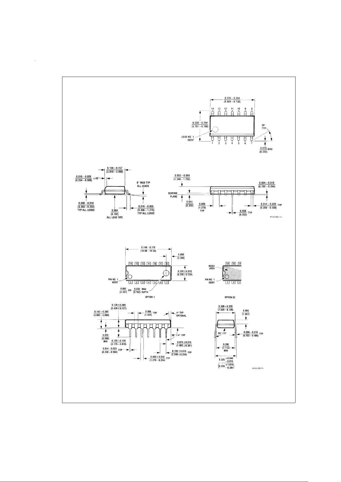
14-Pin Small Outline Molded Package (M)
Order Number LPC660AIM or LPC660IM
NS Package Number M14A
14-Pin Molded Dual-In-Line Package (N)
Order Number LPC660AIN or LPC660IN
NS Package Number N14A
www.national.com 16
Page 17

Notes
LIFE SUPPORT POLICY
NATIONAL’S PRODUCTS ARE NOT AUTHORIZED FOR USE AS CRITICAL COMPONENTS IN LIFE SUPPORT
DEVICES OR SYSTEMS WITHOUT THE EXPRESS WRITTEN APPROVAL OF THE PRESIDENT OF NATIONAL
SEMICONDUCTOR CORPORATION. As used herein:
1. Life support devices or systems are devices or
systems which, (a) are intended for surgical implant
into the body, or (b) support or sustain life, and
whose failure to perform when properly used in
accordance with instructions for use provided in the
labeling, can be reasonably expected to result in a
significant injury to the user.
2. A critical component is any component of a life
support device or system whose failure to perform
can be reasonably expected to cause the failure of
the life support device or system, or to affect its
safety or effectiveness.
National Semiconductor
Corporation
Americas
Tel: 1-800-272-9959
Fax: 1-800-737-7018
Email: [email protected]
National Semiconductor
Europe
Fax: +49 (0) 1 80-530 85 86
Email: [email protected]
Deutsch Tel: +49 (0) 1 80-530 85 85
English Tel: +49 (0) 1 80-532 78 32
Français Tel: +49 (0) 1 80-532 93 58
Italiano Tel: +49 (0) 1 80-534 16 80
National Semiconductor
Asia Pacific Customer
Response Group
Tel: 65-2544466
Fax: 65-2504466
Email: [email protected]
National Semiconductor
Japan Ltd.
Tel: 81-3-5639-7560
Fax: 81-3-5639-7507
www.national.com
LPC660 Low Power CMOS Quad Operational Amplifier
National does not assume any responsibility for use of any circuitry described, no circuit patent licenses are implied and National reserves the right at any time without notice to change said circuitry and specifications.
 Loading...