

Datasheet LP3986TL-3333, LP3986TL-2929, LP3986TL-285285, LP3986TL-2828, LP3986BLX285285 Datasheet (NSC)
...Page 1
LP3986
Dual Micropower 150 mA Ultra Low-Dropout CMOS
Voltage Regulators in micro SMD Package
General Description
The LP3986 is a 150 mA dual low dropout regulator designed for portable and wireless applications with demanding performance and board space requirements.
The LP3986 is stable with a small 1 µF
±
30% ceramic output
capacitor requiring smallest possible board space.
The LP3986’s performance is optimized for battery powered
systems to deliver ultra low noise, extremely low dropout
voltage and low quiescent current independent of load current. Regulator ground current increases very slightly in
dropout, further prolonging the battery life. Optional external
bypass capacitor reduces the output noise further without
slowing down the load transient response. Fast start-up time
is achieved by utilizing a speed-up circuit that actively precharges the bypass capacitor. Power supply rejection is
better than 60 dB at low frequencies and 55 dB at 10 kHz.
High power supply rejection is maintained at low input voltage levels common to battery operated circuits.
The LP3986 is available in a micro SMD package. Performance is specified for a −40˚C to +125˚C temperature
range. For single LDO applications, please refer to the
LP3985 datasheet.
Features
n Miniature 8-I/O micro SMD package
n Stable with 1µF ceramic and high quality tantalum
output capacitors
n Fast turn-on
n Two independent regulators
n Logic controlled enable
n Over current and thermal protection
Key Specifications
n Guaranteed 150 mA output current per regulator
n 1nA typical quiescent current when both regulators in
shutdown mode
n 60 mV typical dropout voltage at 150 mA output current
n 115 µA typical ground current
n 40 µV typical output noise
n 200 µs fast turn-on circuit
n −40˚C to +125˚C junction temperature
Applications
n CDMA cellular handsets
n GSM cellular handsets
n Portable information appliances
n Portable battery applications
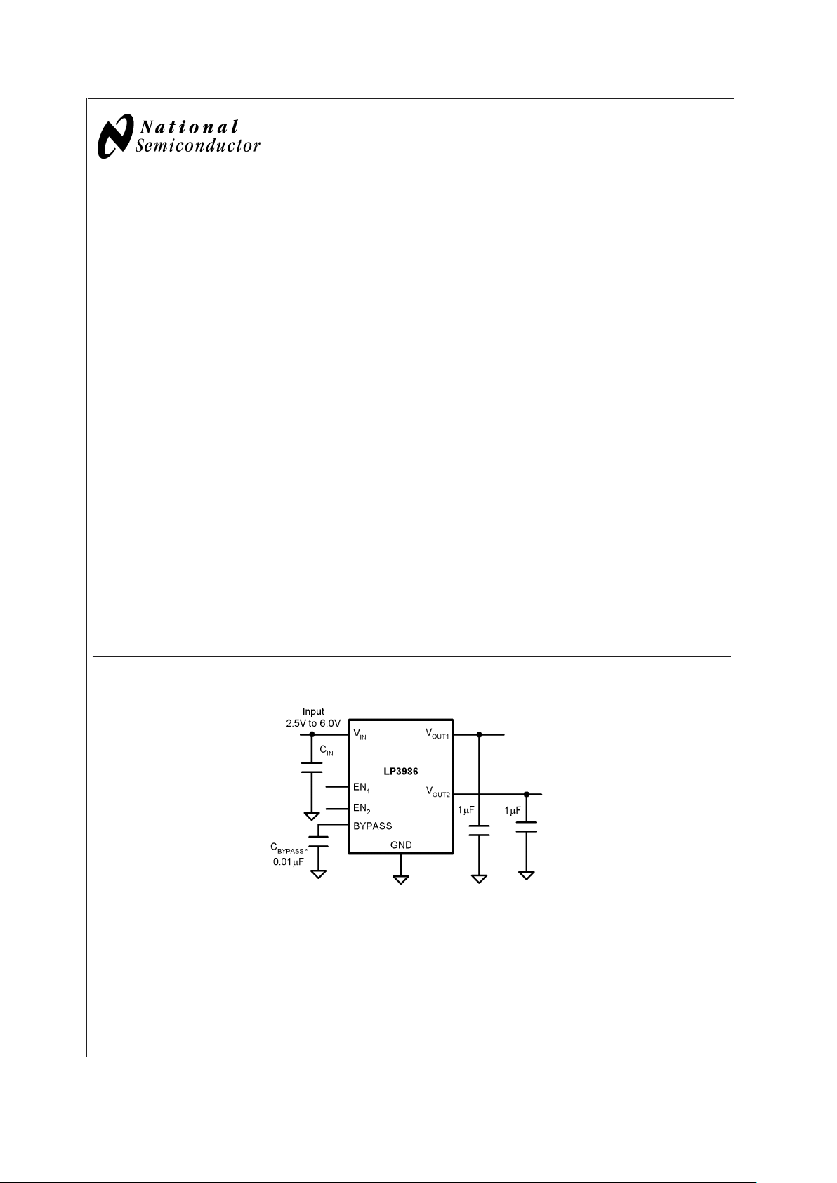
Typical Application Circuit
20003401
May 2003
LP3986 Dual Micropower 150 mA Ultra Low-Dropout CMOS Voltage Regulators in micro SMD
Package
© 2003 National Semiconductor Corporation DS200034 www.national.com
Page 2
Block Diagram
LP3986
20003402
Pin Description
Name *micro SMD Function
V
OUT2
A1 Output Voltage of the second LDO
EN
2
B1 Enable input for the second LDO
BYPASS C1 Bypass capacitor for the bandgap
GND C2 Common ground
GND C3 Common ground
EN
1
B3 Enable input for the first LDO
V
OUT1
A3 Output Voltage of the first LDO
V
IN
A2 Common input for both LDOs
* Note: The pin numbering scheme for the micro SMD package was revised in April 2002 to conform to JEDEC standard. Only the pin
numbers were revised. No changes to the physical location of the inputs/outputs were made. For reference purposes, the obsolete
numbering scheme had V
OUT2
as pin 1, EN2as pin 2, BYPASS as pin 3, GND as pins 4 and 5, EN1as pin 6, V
OUT1
as pin 7, and V
IN
as pin 8.
Connection Diagram
20003404
Top View
8 Bump micro SMD Package
See NS Package Number BLA08
LP3986
www.national.com 2
Page 3
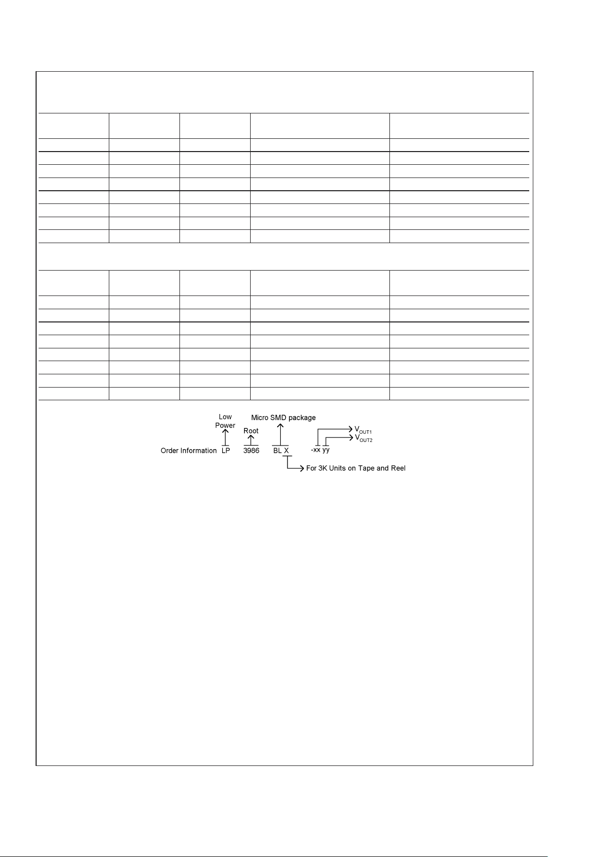
Ordering Information
For micro SMD Package (BL has thickness of 0.995mm)
Output
Voltage (V)
Grade
Package
Marking
LP3986 Supplied as 250 Units,
Tape and Reel
LP3986 Supplied as 3000
Units, Tape and Reel
2.52.8 STD 14 LP3986BL-2528 LP3986BLX-2528
2.82.8 STD 10 LP3986BL-2828 LP3986BLX-2828
2.852.85 STD 11 LP3986BL-285285 LP3986BLX285285
2.92.9 STD 15 LP3986BL-2929 LP3986BLX-2929
3.03.0 STD 12 LP3986BL-3030 LP3986BLX-3030
3.13.1 STD 13 LP3986BL-3131 LP3986BLX-3131
3.13.3 STD 16 LP3986BL-3133 LP3986BLX-3133
3.33.3 STD 17 LP3986BL-3333 LP3986BLX-3333
For micro SMD Package (TL has thickness of 0.600mm)
Output
Voltage (V)
Grade
Package
Marking
LP3986 Supplied as 250 Units,
Tape and Reel
LP3986 Supplied as 3000
Units, Tape and Reel
2.52.8 STD 14 LP3986TL-2528 LP3986TLX-2528
2.82.8 STD 10 LP3986TL-2828 LP3986TLX-2828
2.852.85 STD 11 LP3986TL-285285 LP3986TLX285285
2.92.9 STD 15 LP3986TL-2929 LP3986TLX-2929
3.03.0 STD 12 LP3986TL-3030 LP3986TLX-3030
3.13.1 STD 13 LP3986TL-3131 LP3986TLX-3131
3.13.3 STD 16 LP3986TL-3133 LP3986TLX-3133
3.33.3 STD 17 LP3986TL-3333 LP3986TLX-3333
20003403
LP3986
www.national.com3
Page 4
Absolute Maximum Ratings (Notes 1,
2)
If Military/Aerospace specified devices are required,
please contact the National Semiconductor Sales Office/
Distributors for availability and specifications.
V
IN,VEN
−0.3 to 6.5V
V
OUT
−0.3 to (VIN+0.3V) ≤ 6.5V
Junction Temperature 150˚C
Storage Temperature −65˚C to +150˚C
Pad Temp. (Note 3) 235˚C
Maximum Power Dissipation
(Note 4) 364mW
ESD Rating (Note 5)
Human Body Model
Machine Model
2kV
200V
Operating Ratings (Notes 1, 2)
V
IN
2.5 to 6V
V
EN
0to(VIN+ 0.3V) ≤ 6V
Junction Temperature −40˚C to +125˚C
Thermal Resistance
θ
JA
220˚C/W
Maximum Power Dissipation (Note 6) 250mW
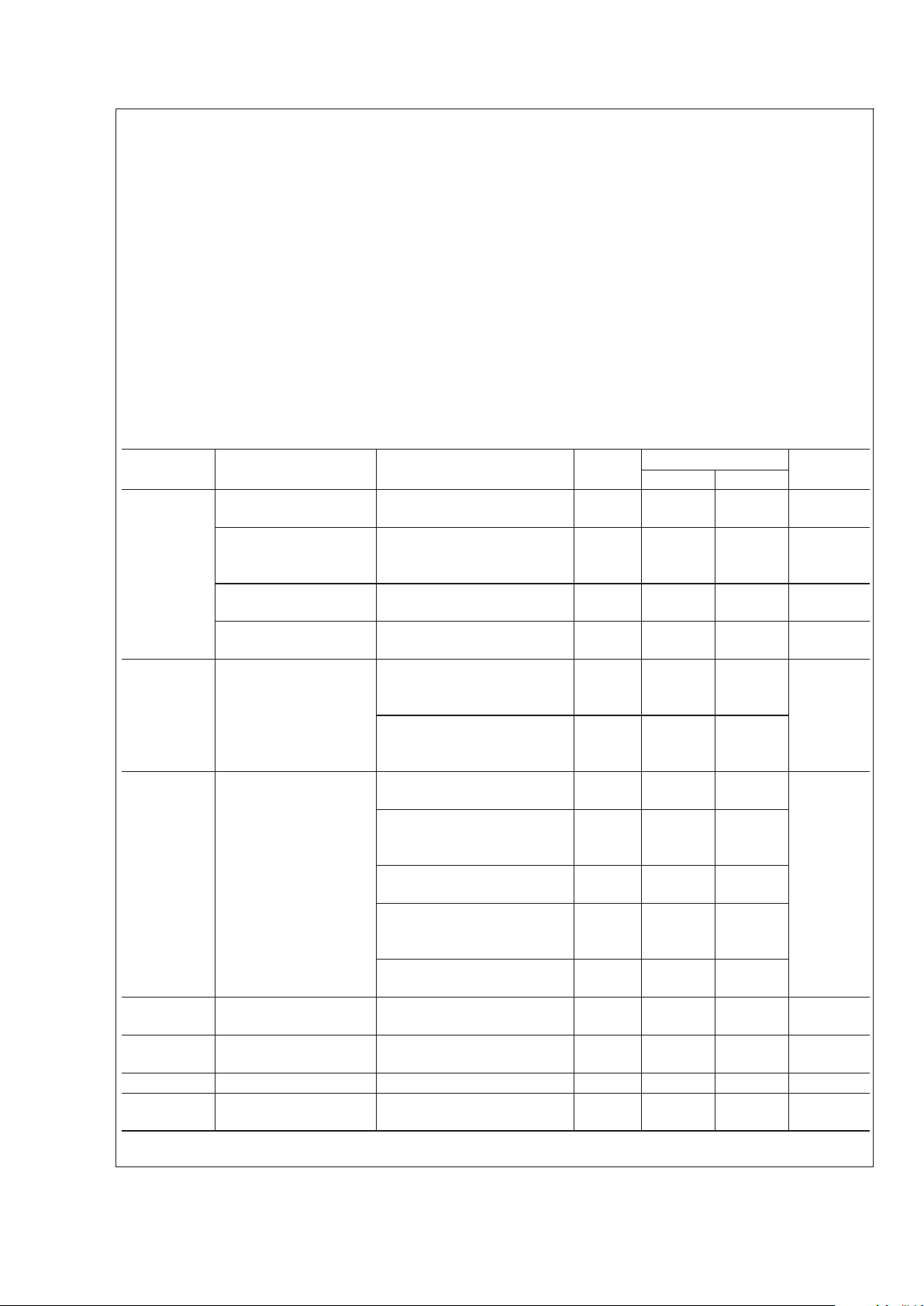
Electrical Characteristics
Unless otherwise specified: VIN=V
OUT(nom)
+ 0.5V, CIN= 1 µF, I
OUT
= 1mA, C
OUT
= 1 µF, C
BYPASS
= 0.01µF. Typical values
and limits appearing in standard typeface are for T
J
= 25˚C. Limits appearing in boldface type apply over the entire junction
temperature range for operation, −40˚C to +125˚C. (Note 7) (Note 8)
Symbol Parameter Conditions Typ
Limit
Units
Min Max
∆V
OUT
Output Voltage
Tolerance
I
OUT
= 1mA −2.5
−3.0
2.5
3.0
%of
V
OUT(nom)
Line Regulation Error
(Note 9)
VIN=(V
OUT(nom)
+ 0.5V) to
6.0V,
I
OUT
=1mA
0.006 0.092
0.128 %/V
Load Regulation Error
(Note 10)
I
OUT
= 1mA to 150 mA 0.003 0.006
0.01
%/mA
Output AC Line
Regulation
VIN=V
OUT(nom)
+ 1V,
I
OUT
= 150 mA (Figure 1)
1.5
mV
P-P
PSRR
Power Supply Rejection
Ratio
V
IN
= 3.1V,
f = 1 kHz,
I
OUT
=50mA(Figure 2)
60
dB
V
IN
= 3.1V,
f = 10 kHz,
I
OUT
=50mA(Figure 2)
50
I
Q
Quiescent Current Both Regulators ON
V
EN
= 1.4V, I
OUT
=0mA
115 200
µA
Both Regulators ON
V
EN
= 1.4V, I
OUT
= 0 to 150
mA
220 320
One Regulator ON
V
EN
= 1.4V I
OUT
=0mA
75 130
One Regulator ON
VEN= 1.4V I
OUT
= 0 to 150
mA
130 200
V
EN
= 0.4V, Both Regulators
OFF (shutdown)
0.001 2
4
Dropout Voltage
(Note 11)
I
OUT
=1mA
I
OUT
= 150 mA
0.4
60
2
100
mV
I
SC
Short Circuit Current
Limit
Output Grounded 600
mA
I
OUT(PK)
Peak Output Current V
OUT
≥ V
OUT(nom)
- 5% 500 300 mA
T
ON
Turn-On Time
(Note 12)
C
BYPASS
= 0.01 µF 200
µs
LP3986
www.national.com 4
Page 5

Electrical Characteristics (Continued)
Unless otherwise specified: VIN=V
OUT(nom)
+ 0.5V, CIN= 1 µF, I
OUT
= 1mA, C
OUT
= 1 µF, C
BYPASS
= 0.01µF. Typical values
and limits appearing in standard typeface are for T
J
= 25˚C. Limits appearing in boldface type apply over the entire junction
temperature range for operation, −40˚C to +125˚C. (Note 7) (Note 8)
Symbol Parameter Conditions Typ
Limit
Units
Min Max
e
n
Output Noise Voltage BW = 10 Hz to 100 kHz,
C
OUT
= 1µF
40 µVrms
ρn(1/f) Output Noise Density f = 120 Hz,
C
OUT
= 1µF
1 µV/
I
EN
Maximum Input Current
at EN
VEN= 0.4 and VIN=6V
±
10 nA
V
IL
Maximum Low Level
Input Voltage at EN
VIN= 2.5 to 6V 0.4 V
V
IH
Minimum High Level
Input Voltage at EN
VIN= 2.5 to 6V 1.4 V
Xtalk Crosstalk Rejection
∆I
Load1
= 150 mA at 1KHz rate
∆I
Load2
=1mA
∆V
OUT2
/∆V
OUT1
−60
dB
∆I
Load2
= 150 mA at 1KHz rate
∆I
Load1
=1mA
∆V
OUT2
/∆V
OUT1
−60
C
OUT
Capacitance (Note 13) 122µF
ESR (Note 14) 5 500 mΩ
Note 1: Absolute Maximum Ratings are limits beyond which damage to the device may occur. Operating Ratings are conditions under which operation of the device
is guaranteed. Operating Ratings do not imply guaranteed performance limits. For guaranteed performance limits and associated test conditions, see the Electrical
Characteristics tables.
Note 2: All voltages are with respect to the potential at the GND pin.
Note 3: Additional information on pad temperature can be found in National Semiconductor Application Note (AN-1112).
Note 4: The Absolute Maximum power dissipation depends on the ambient temperature and can be calculated using the formula:
PD=(TJ-TA)/θJA,
Where TJis the junction temperature, TAis the ambient temperature, and θJAis the junction-to-ambient thermal resistance. The 364mW rating appearing under
Absolute Maximum Ratings results from substituting the Absolute Maximum junction temperature, 150˚C, for T
J
, 70˚C for TA, and 220˚C/W for θJA. More power can
be dissipated safely at ambient temperatures below 70˚C . Less power can be dissipated safely at ambient temperatures above 70˚C. TheAbsolute Maximum power
dissipation can be increased by 4.5mW for each degree below 70˚C, and it must be derated by 4.5mW for each degree above 70˚C.
Note 5: The human body model is 100pF discharged through a 1.5kΩ resistor into each pin. The machine model is a 200pF capacitor discharged directly into each
pin.
Note 6: Like the Absolute Maximum power dissipation, the maximum power dissipation for operation depends on the ambient temperature. The 250mW rating
appearing under Operating Ratings results from substituting the maximum junction temperature for operation, 125˚C, for T
J
, 70˚C for TA, and 220˚C/W for θJAinto
(1) above. More power can be dissipated at ambient temperatures below 70˚C . Less power can be dissipated at ambient temperatures above 70˚C. The maximum
power dissipation for operation can be increased by 4.5mW for each degree below 70˚C, and it must be derated by 4.5mW for each degree above 70˚C.
Note 7: All limits are guaranteed. All electrical characteristics having room temperature limits are tested during production with T
J
= 25˚C or correlated using
Statistical Quality Control (SQC) methods. All hot and cold limits are guaranteed by correlating the electrical characteristics to process and temperature variations
and applying statistical process control.
Note 8: The target output voltage, which is labeled V
OUT(nom)
, is the desired voltage option.
Note 9: The output voltage changes slightly with line voltage. An increase in the line voltage results in a slight increase in the output voltage and vice versa.
Note 10: The output voltage changes slightly with load current. An increase in the load current results in a slight decrease in the output voltage and vice versa.
Note 11: Dropout voltage is the input-to-output voltage difference at which the output voltage is 100mV below its nominal value.
Note 12: Turn-on time is that between the enable input just exceeding V
IH
and the output voltage just reaching 95% of its nominal value.
Note 13: Range of capacitor values for which the device will remain stable. This electrical specification is guaranteed by design.
Note 14: Range of capacitor ESR values for which the device will remain stable. This electrical specification is guaranteed by design.
LP3986
www.national.com5
Page 6

20003408
FIGURE 1. Line Regulation Input Test Signal
20003409
FIGURE 2. PSRR Input Test Signal
LP3986
www.national.com 6
Page 7

Typical Performance Characteristics Unless otherwise specified, C
IN=COUT
1µF Ceramic, CBP=
0.01µ F, V
IN=VOUT
+ 0.5, TA= 25˚C, both enable pins are tied to V
IN
Power Supply Rejection Ratio (CBP= 0.001µF) Power Supply Rejection Ratio (CBP= 0.01µF)
20003410 20003447
Power Supply Rejection Ratio (CBP= 0.1µF) Output Noise Spectral Density
20003448 20003451
Line Transient Response (CBP= 0.001µF) Line Transient Response (CBP= 0.01µF)
20003413 20003449
LP3986
www.national.com7
Page 8

Typical Performance Characteristics Unless otherwise specified, C
IN=COUT
1µF Ceramic, CBP=
0.01µ F, V
IN=VOUT
+ 0.5, TA= 25˚C, both enable pins are tied to VIN(Continued)
Load Transient & Cross Talk (V
IN=VOUT
+ 0.2V) Load Transient & Cross Talk (VIN=V
OUT
+ 0.2V)
20003417 20003416
Start-Up Time (CBP= 0.001, 0.01, 0.1µF) Enable Response ( VIN= 4.2V )
20003411
20003414
Enable Response (VIN=V
OUT
+ 0.2V) Enable Response
20003415
20003450
LP3986
www.national.com 8
Page 9

Typical Performance Characteristics Unless otherwise specified, C
IN=COUT
1µF Ceramic, CBP=
0.01µ F, V
IN=VOUT
+ 0.5, TA= 25˚C, both enable pins are tied to VIN(Continued)
Output Short Circuit Current at V
IN
= 6V Output Short Circuit Current at VIN= 3.3V
20003465 20003466
LP3986
www.national.com9
Page 10

Application Hints
EXTERNAL CAPACITORS
Like any low-dropout regulator, the LP3986 requires external
capacitors for regulator stability. The LP3986 is specifically
designed for portable applications requiring minimum board
space and smallest components. These capacitors must be
correctly selected for good performance.
INPUT CAPACITOR
An input capacitance of ) 1µF is required between the
LP3986 input pin and ground (the amount of the capacitance
may be increased without limit).
This capacitor must be located a distance of not more than
1cm from the input pin and returned to a clean analog
ground. Any good quality ceramic, tantalum, or film capacitor
may be used at the input.
Important: Tantalum capacitors can suffer catastrophic failures due to surge current when connected to a lowimpedance source of power (like a battery or a very large
capacitor). If a tantalum capacitor is used at the input, it must
be guaranteed by the manufacturer to have a surge current
rating sufficient for the application.
There are no requirements for the ESR on the input capacitor, but tolerance and temperature coefficient must be considered when selecting the capacitor to ensure the capacitance will be ) 1µF over the entire operating temperature
range.
OUTPUT CAPACITOR
The LP3986 is designed specifically to work with very small
ceramic output capacitors, any ceramic capacitor (temperature characteristics X7R, X5R, Z5U or Y5V) in 1 to 22 µF
range with 5mΩ to 500mΩ ESR range is suitable in the
LP3986 application circuit.
It may also be possible to use tantalum or film capacitors at
the output, but these are not as attractive for reasons of size
and cost (see next section Capacitor Characteristics).
The output capacitor must meet the requirement for minimum amount of capacitance and also have an ESR (Equivalent Series Resistance) value which is within a stable range.
NO-LOAD STABILITY
The LP3986 will remain stable and in regulation with no-load
(other than the internal voltage divider). This is specially
important in CMOS RAM keep-alive applications.
CAPACITOR CHARACTERISTICS
The LP3986 is designed to work with ceramic capacitors on
the output to take advantage of the benefits they offer: for
capacitance values in the range of 1µF to 4.7µF range,
ceramic capacitors are the smallest, least expensive and
have the lowest ESR values (which makes them best for
eliminating high frequency noise). The ESR of a typical 1µF
ceramic capacitor is in the range of 20 mΩ to 40 mΩ, which
easily meets the ESR requirement for stability by the
LP3986.
The ceramic capacitor’s capacitance can vary with temperature. The capacitor type X7R, which operates over a temperature range of -55˚C to +125˚C, will only vary the capacitance to within
±
15%. Most large value ceramic capacitors
() 2.2µF) are manufactured with Z5U or Y5V temperature
characteristics. Their capacitance can drop by more than
50% as the temperature goes from 25˚C to 85˚C. Therefore,
X7R is recommended over Z5U and Y5 in applications
where the ambient temperature will change significantly
above or below 25˚C.
Tantalum capacitors are less desirable than ceramic for use
as output capacitors because they are more expensive when
comparing equivalent capacitance and voltage ratings in the
1µF to 4.7µF range.
Another important consideration is that tantalum capacitors
have higher ESR values than equivalent size ceramics. This
means that while it may be possible to find a tantalum
capacitor with an ESR value within the stable range, it would
have to be larger in capacitance (which means bigger and
more costly ) than a ceramic capacitor with the same ESR
value. It should also be noted that the ESR of a typical
tantalum will increase about 2:1 as the temperature goes
from 25˚C down to −40˚C, so some guard band must be
allowed.
NOISE BYPASS CAPACITOR
Connecting a 0.01µF capacitor between the C
BYPASS
pin
and ground significantly reduces noise on the regulator output. This cap is connected directly to a high impedance node
in the band gap reference circuit. Any significant loading on
this node will cause a change on the regulated output voltage. For this reason, DC leakage current through this pin
must be kept as low as possible for best output voltage
accuracy. The use of this 0.01µF bypass capacitor is strongly
recommended to prevent overshoot on the output during
start up.
The types of capacitors best suited for the noise bypass
capacitor are ceramic and film. High-quality ceramic capacitors with either NPO or COG dielectric typically have very
low leakage. Polypropolene and polycarbonate film capacitors are available in small surface-mount packages and
typically have extremely low leakage current.
Unlike many other LDO’s, addition of a noise reduction
capacitor does not effect the transient response of the device.
ON/OFF INPUT OPERATION
The LP3986 is turned off by pulling the V
EN
pin low, and
turned on by pulling it high. If this feature is not used, the V
EN
pin should be tied to VINto keep the regulator output on at all
times. To assure proper operation, the signal source used to
drive the V
EN
input must be able to swing above and below
the specified turn-on/off voltage thresholds listed in the Electrical Characteristics section under V
IL
and VIH.
FAST ON-TIME
The LP3986 outputs are turned on after V
ref
voltage reaches
its final value (1.23V nominal). To speed up this process, the
noise reduction capacitor at the bypass pin is charged with
an internal 70µAcurrent source. The current source is turned
off when the bandgap voltage reaches approximately 95% of
its final value. The turn on time is determined by the time
constant of the bypass capccitor. The smaller the capacitor
value, the shorter the turn on time, but less noise gets
reduced. As a result, turn on time and noise reduction need
to be taken into design consideration when choosing the
value of the bypass capacitor.
LP3986
www.national.com 10
Page 11

Application Hints (Continued)
MICRO SMD MOUNTING
The micro SMD package requires specific mounting techniques which are detailed in National Semiconductor Application Note (AN-1112). Referring to the section Surface
Mount Technology (SMT) Assembly Considerations.
For best results during assembly, alignment ordinals on the
PC board may be used to facilitate placement of the micro
SMD device.
MICRO SMD LIGHT SENSITIVITY
Exposing the micro SMD device to direct sunlight will cause
misoperation of the device. Light sources such as halogen
lamps can effect electrical performance if brought near to the
device.
The wavelengths which have most detrimental effect are
reds and infra-reds, which means that the fluorescent lighting used inside most buildings has very little effect on performance. A micro SMD test board was brought to within
1cm of a fluorescent desk lamp and the effect on the regulated output voltage was negligible, showing a deviation of
less than 0.1% from nominal.
LP3986
www.national.com11
Page 12

Physical Dimensions inches (millimeters) unless otherwise noted
micro SMD, 8 Bump
NS Package Number BLA08CCC
The dimensions for X1, X2 and X3 are as follows:
X1 = 1.55mm
X2 = 1.55mm
X3 = 0.995mm
LP3986
www.national.com 12
Page 13

Physical Dimensions inches (millimeters) unless otherwise noted (Continued)
micro SMD, 8 Bump
NS Package Number ATL08CCA
The dimensions for X1, X2 and X3 are as follows:
X1 = 1.55mm
X2 = 1.55mm
X3 = 0.600mm
LIFE SUPPORT POLICY
NATIONAL’S PRODUCTS ARE NOT AUTHORIZED FOR USE AS CRITICAL COMPONENTS IN LIFE SUPPORT
DEVICES OR SYSTEMS WITHOUT THE EXPRESS WRITTEN APPROVAL OF THE PRESIDENT AND GENERAL
COUNSEL OF NATIONAL SEMICONDUCTOR CORPORATION. As used herein:
1. Life support devices or systems are devices or
systems which, (a) are intended for surgical implant
into the body, or (b) support or sustain life, and
whose failure to perform when properly used in
accordance with instructions for use provided in the
labeling, can be reasonably expected to result in a
significant injury to the user.
2. A critical component is any component of a life
support device or system whose failure to perform
can be reasonably expected to cause the failure of
the life support device or system, or to affect its
safety or effectiveness.
National Semiconductor
Americas Customer
Support Center
Email: new.feedback@nsc.com
Tel: 1-800-272-9959
National Semiconductor
Europe Customer Support Center
Fax: +49 (0) 180-530 85 86
Email: europe.support@nsc.com
Deutsch Tel: +49 (0) 69 9508 6208
English Tel: +44 (0) 870 24 0 2171
Français Tel: +33 (0) 1 41 91 8790
National Semiconductor
Asia Pacific Customer
Support Center
Email: ap.support@nsc.com
National Semiconductor
Japan Customer Support Center
Fax: 81-3-5639-7507
Email: jpn.feedback@nsc.com
Tel: 81-3-5639-7560
www.national.com
LP3986 Dual Micropower 150 mA Ultra Low-Dropout CMOS Voltage Regulators in micro SMD
Package
National does not assume any responsibility for use of any circuitry described, no circuit patent licenses are implied and National reserves the right at any time without notice to change said circuitry and specifications.
 Loading...