

Page 1
LP3982
Micropower, Ultra Low-Dropout, Low-Noise, 300mA
CMOS Regulator
LP3982 Micropower, Ultra Low-Dropout, Low-Noise, 300mA CMOS Regulator
March 2006
General Description
The LP3982 low-dropout (LDO) CMOS linear regulator is
available in 1.8V, 2.5V, 2.77V, 2.82V, 3.0V, 3.3V, and adjustable versions. They deliver 300mA of output current. Packaged in an 8-Pin MSOP, the LP3982 is pin and package
compatible with Maxim’s MAX8860. The LM3982 is also
available in the small footprint LLP package.
The LP3982 suits battery powered applications because of
its shutdown mode (1nA typ), low quiescent current (90µA
typ), and LDO voltage (120mV typ). The low dropout voltage
allows for more utilization of a battery’s available energy by
operating closer to its end-of-life voltage. The LP3982’s
PMOS output transistor consumes relatively no drive current
compared to PNP LDO regulators.
This PMOS regulator is stable with small ceramic capacitive
loads (2.2µF typ).
These devices also include regulation fault detection, a
bandgap voltage reference, constant current limiting and
thermal overload protection.
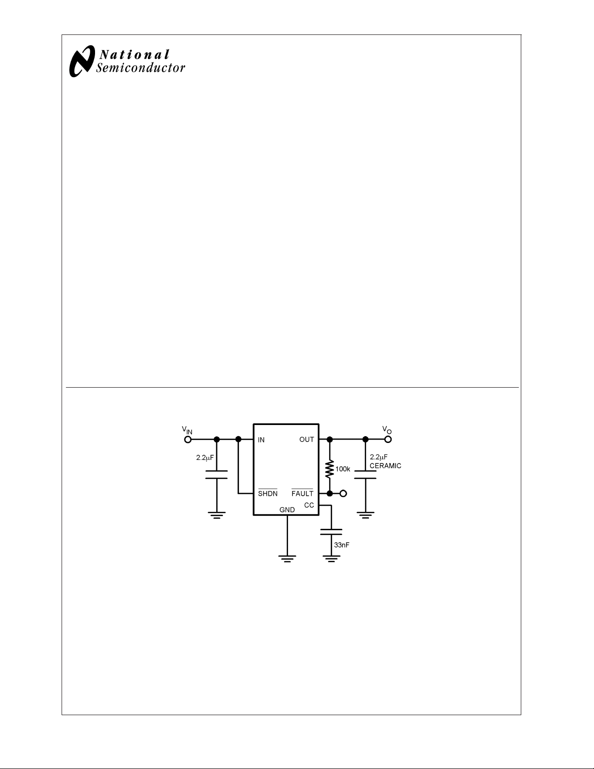
Application Circuit
Features
n MAX8860 pin, package and spec. compatible
n LLP space saving package
n 300mA guaranteed output current
n 120mV typical dropout
n 90µA typical quiescent current
n 1nA typical shutdown mode
n 60dB typical PSRR
n 2.5V to 6V input range
n 120µs typical turn-on time
n Stable with small ceramic output capacitors
n 37µV RMS output voltage noise (10Hz to 100kHz)
n Over temperature/over current protection
±
n
2% output voltage tolerance
@
300mA
Applications
n Wireless handsets
n DSP core power
n Battery powered electronics
n Portable information appliances
20036931
© 2006 National Semiconductor Corporation DS200369 www.national.com
Page 2
Absolute Maximum Ratings (Notes 1, 2)
If Military/Aerospace specified devices are required,
LP3982
please contact the National Semiconductor Sales Office/
Distributors for availability and specifications.
V
IN,VOUT,VSHDN,VSET,VCC
V
FAULT
,
−0.3V to 6.5V
ESD Rating
Human Body Model (Note 6) 2kV
Machine Model 200V
Thermal Resistance (θ
)
JA
8-Pin MSOP 223˚C/W
8-Pin LLP (Note 3)
Fault Sink Current 20mA
Power Dissipation (Note 3)
Storage Temperature Range −65˚C to 160˚C
Junction Temperature (T
) 150˚C
J
Lead Temperature (10 sec.) 260˚C
Operating Ratings(Note 1), (Note 2)
Temperature Range −40˚C to 85˚C
Supply Voltage 2.5V to 6.0V
Electrical Characteristics
Unless otherwise specified, all limits guaranteed for VIN=VO+0.5V (Note 7), V
TJ= 25˚C. Boldface limits apply for the operating temperature extremes: −40˚C and 85˚C.
Symbol Parameter Conditions Min
V
∆V
IN
O
Input Voltage 2.5 6.0 V
Output Voltage Tolerance 100µA ≤ I
V
IN=VO
≤ 300mA
OUT
+0.5V, (Note 7)
SET = OUT for the Adjust
Versions
V
I
O
I
LIMIT
I
Q
V
∆V
O
DO
O
Output Adjust Range Adjust Version Only 1.25 6 V
Maximum Output Current Average DC Current Rating 300 mA
Output Current Limit 330 770 mA
Supply Current I
Shutdown Supply Current V
Dropout Voltage
(Note 7), (Note 8)
Line Regulation I
= 0mA 90 270
OUT
I
= 300mA 225
OUT
= 0V, SHDN = GND 0.001 1 µA
O
I
= 1mA 0.4
OUT
= 200mA 80 220
OUT
I
= 300mA 120
OUT
= 1mA, (VO+ 0.5V) ≤ VI≤ 6V
OUT
(Note 7)
e
V
n
SHDN
Load Regulation 100µA ≤ I
Output Voltage Noise I
= 10mA, 10Hz ≤ f ≤ 100kHz 37 µV
OUT
Output Voltage Noise Density 10Hz ≤ f ≤ 100kHz, C
SHDN Input Threshold VIH,(VO+ 0.5V) ≤ VI≤ 6V
≤ 300mA 0.002 %/mA
OUT
= 10µF 190 nV/
OUT
(Note 7)
,(VO+ 0.5V) ≤ VI≤ 6V
V
IL
(Note 7)
I
SHDN
I
SET
SHDN Input Bias Current SHDN = GND or IN 0.1 100 nA
SET Input Leakage SET = 1.3V, Adjust Version Only
(Note 9)
V
FAULT
FAULTDetection Voltage VO≥ 2.5V, I
OUT
= 200mA
(Note 10)
I
= 2mA 0.115 0.25 V
SINK
I
FAULT
T
SD
FAULT Output Low Voltage
FAULT Off-Leakage Current FAULT = 3.6V, SHDN = 0V 0.1 100 nA
Thermal Shutdown
Temperature
Thermal Shutdown Hysteresis 10
T
ON
Start-Up Time C
= 10µF, VOat 90% of Final
OUT
Value
Note 1: Absolute Maximum ratings indicate limits beyond which damage may occur. Electrical specifications do not apply when operating the device outside of its
rated operating conditions.
=VIN,CIN=C
SHDN
(Note 5)
Typ
(Note 4)
= 2.2µF, CCC= 33nF,
OUT
Max
(Note 5)
−2 +2
−3 +3
−0.1 0.01 0.1 %/V
2
0.4
0.1 2.5 nA
120 280 mV
160
120 µs
Units
%of
V
OUT (NOM)
µA
mVI
RMS
V
˚C
www.national.com 2
Page 3
Electrical Characteristics (Continued)
Note 2: All voltages are with respect to the potential at the ground pin.
Note 3: Maximum Power dissipation for the device is calculated using the following equations:
LP3982
where T
package θ
thus below 25˚C the power dissipation figure can be increased by 4.5mW per degree, and similarity decreased by this factor for temperatures above 25˚C. The value
of the θ
resistance and power dissipation for the LLP package, refer to Application Note AN-1187.
Note 4: Typical Values represent the most likely parametric norm.
Note 5: All limits are guaranteed by testing or statistical analysis.
Note 6: Human body model: 1.5kΩ in series with 100pF.
Note 7: Condition does not apply to input voltages below 2.5V since this is the minimum input operating voltage.
Note 8: Dropout voltage is measured by reducing V
version.
Note 9: The SET pin is not externally connected for the fixed versions.
Note 10: The FAULT detection voltage is specified for the input to output voltage differential at which the FAULT pin goes active low.
is the maximum junction temperature, TAis the ambient temperature, and θJAis the junction-to-ambient thermal resistance. E.g. for the MSOP-8
J(MAX)
= 223˚C/W, T
JA
for the LLP package is specifically dependent on the PCB trace area, trace material, and the number of layers and thermal vias. For improved thermal
JA
= 150˚C and using TA= 25˚C, the maximum power dissipation is found to be 561mW. The derating factor (−1/θJA) = −4.5mW/˚C,
J(MAX)
until VOdrops 100mV from its nominal value at VIN-VO= 0.5V. Dropout Voltage does not apply to the 1.8
IN
Functional Block Diagram
20036913
www.national.com3
Page 4
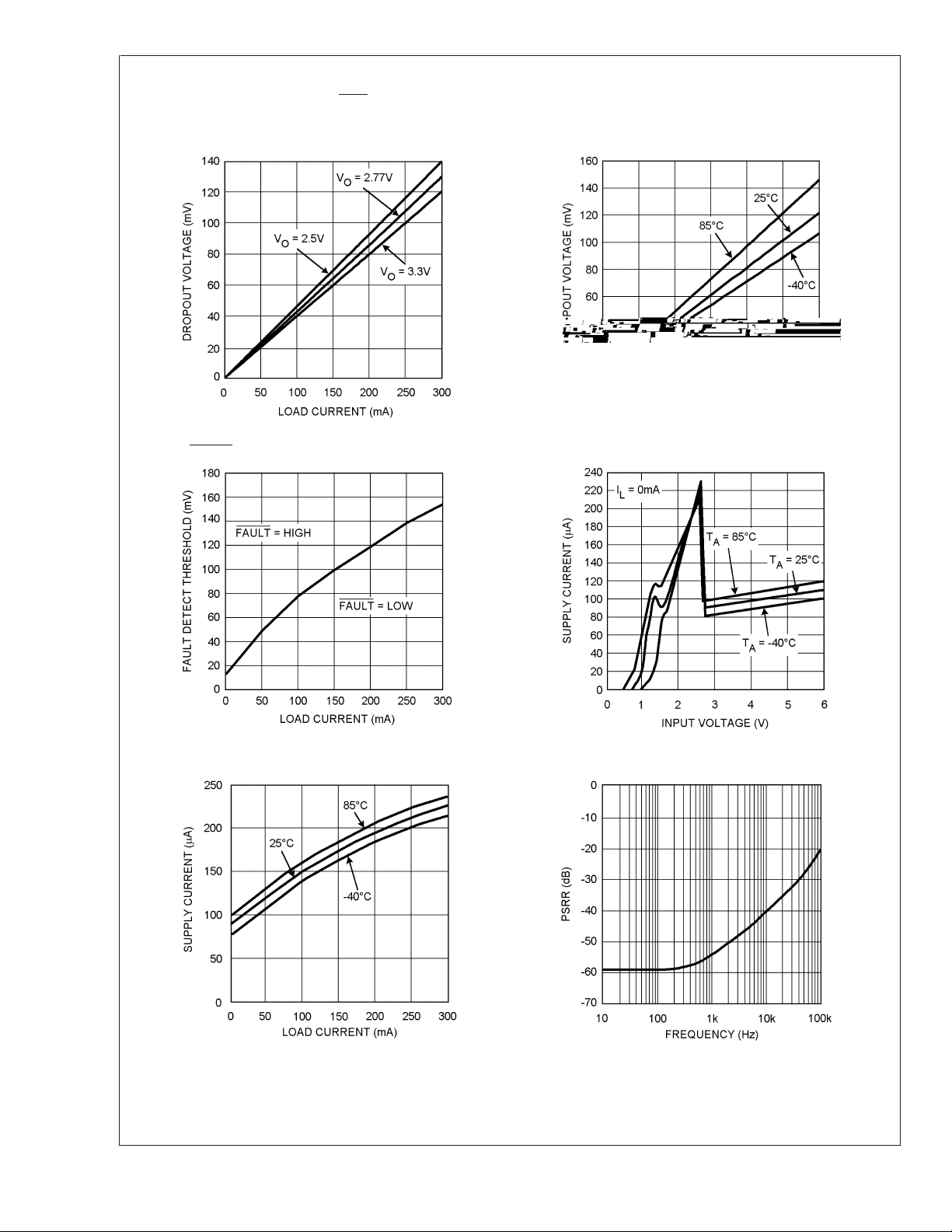
Typical Performance Characteristics Unless otherwise specified, V
2.2µF, C
LP3982
= 33nF, TJ= 25˚C, V
CC
SHDN=VIN
Dropout Voltage vs. Load Current
(For Different Output Voltages)
FAULT Detect Threshold vs. Load Current Supply Current vs. Input Voltage
.
Dropout Voltage vs. Load Current
(For Different Output Temperatures)
20036903 20036927
IN=VO
+ 0.5V, CIN=C
OUT
=
20036928
Supply Current vs. Load Current Power Supply Rejection Ratio vs. Frequency
20036930
www.national.com 4
20036929
20036904
Page 5

LP3982
Typical Performance Characteristics Unless otherwise specified, V
2.2µF, C
= 33nF, TJ= 25˚C, V
CC
Output Noise Spectral Density Output Noise (10Hz to 100kHz)
Output Impedance vs. Frequency Line Transient Response
=VIN. (Continued)
SHDN
20036905
IN=VO
+ 0.5V, CIN=C
20036906
OUT
=
20036907
Load Transient Shutdown Response
20036909
20036908
20036910
www.national.com5
Page 6

Typical Performance Characteristics Unless otherwise specified, V
2.2µF, C
LP3982
= 33nF, TJ= 25˚C, V
CC
Power-Up Response Power-Down Response
SHDN=VIN
. (Continued)
IN=VO
+ 0.5V, CIN=C
OUT
=
20036911
Application Information
GENERAL INFORMATION
LP3982 is package, pin and performance compatible with
Maxim’s MAX8860 excluding reverse battery protection and
Dual Mode
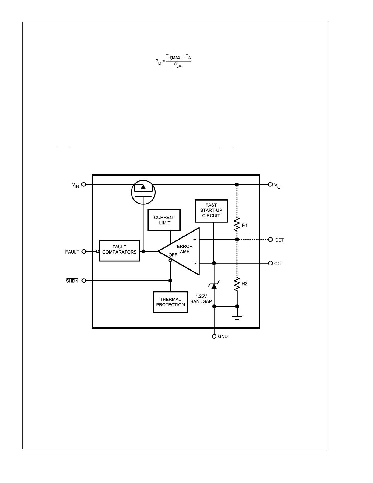
Figure 1 shows the functional block diagram for the LP3982.
A 1.25V bandgap reference, an error amplifier and a PMOS
pass transistor perform voltage regulation while being supported by shutdown, fault, and the usual Temperature and
current protection circuitry
The regulator’s topology is the classic type with negative
feedback from the output to one of the inputs of the error
amplifier. Feedback resistors R
external to the IC, depending on whether it is the fixed
voltage version or the adjustable version. The negative feedback and high open loop gain of the error amplifier cause the
two inputs of the error amplifier to be virtually equal in
voltage. If the output voltage changes due to load changes,
the error amplifier provides the appropriate drive to the pass
transistor to maintain the error amplifier’s inputs as virtually
equal. In short, the error amplifier keeps the output voltage
constant in order to keep its inputs equal.
™
function (fixed and adjustable combined).
and R2are either internal or
1
20036912
OUTPUT VOLTAGE SETTING (ADJ VERSION ONLY)
The output voltage is set according to the amount of negative feedback (Note that the pass transistor inverts the feedback signal.) Figure 2 simplifies the topology of the LP3982.
This type of regulator can be represented as an op amp
configured as non-inverting amplifier and a fixed DC Voltage
) for its input signal. The special characteristic of this
(V
REF
op amp is its extra-large output transistor that only sources
current. In terms of its non-inverting configuration, the output
voltage equals V
times the closed loop gain:
REF
Utilize the following equation for adjusting the output to a
particular voltage:
Choose R2= 100k to optimize accuracy, power supply rejection, noise and power consumption.
20036913
FIGURE 1. Functional Block Diagram for the LP3982
www.national.com 6
20036916
FIGURE 2. Regulator Topology Simplified
Page 7

Application Information (Continued)
Similarity in the output capabilities exists between op amps
and linear regulators. Just as rail-to-rail output op amps
allow their output voltage to approach the supply voltage,
low dropout regulators (LDOs) allow their output voltage to
operate close to the input voltage. Both achieve this by the
configuration of their output transistors. Standard op amps
and regulator outputs are at the source (or emitter) of the
output transistor. Rail-to-rail op amp and LDO regulator outputs are at the drain (or collector) of the output transistor.
This replaces the threshold (or diode drop) limitations on the
output with the less restrictive source-to-drain (or V
tations. There is a trade-off, of course. The output impedance become significantly higher, thus providing a critically
lower pole when combined with the capacitive load. That’s
why rail-to-rail op amps are usually poor at driving capacitive
loads and recommend a series output resistor when doing
so. LDOs require the same series resistance except that the
internal resistance of the output capacitor will usually suffice.
Refer to the output capacitance section for more information.
SAT
) limi-
LP3982
20036917
FIGURE 3. Simplified Model of Regulator
Loop Gain Components
OUTPUT CAPACITANCE
The LP3982 is specifically designed to employ ceramic output capacitors as low as 2.2µF. Ceramic capacitors below
10µF offer significant cost and space savings, along with
high frequency noise filtering. Higher values and other types
and of capacitor may be used, but their equivalent series
resistance (ESR) should be maintained below 0.5Ω
Ceramic capacitor of the value required by the LP3982 are
available in the following dielectric types: Z5U, Y5V, X5R and
X7R. The Z5U and Y5V types exhibit a 50% or more drop in
capacitance value as their temperature increases from 25˚C,
an important consideration. The X5R generally maintain their
±
capacitance value within
20%. The X7R type are desirable
for their tighter tolerance of 10% over temperature.
Ceramic capacitors pose a challenge because of their rela-
tively low ESR. Like most other LDOs, the LP3982 relies on
a zero in the frequency response to compensate against
excessive phase shift in the regulator’s feedback loop. If the
phase shift reaches 360˚ (i.e.; becomes positive), the regulator will oscillate. This compensation usually resides in the
zero generated by the combination of the output capacitor
with its equivalent series resistance (ESR). The zero is
intended to cancel the effects of the pole generated by the
load capacitance (C
tion of the load resistance (R
) of the regulator. The challenge posed by low ESR
(R
O
) combined with the parallel combina-
L
) and the output resistance
L
capacitors is that the zero it generates can be too high in
frequency for the pole that it’s intended to compensate. The
LP3982 overcomes this challenge by internally generating a
strategically placed zero.
Figure 3 shows a basic model for the linear regulator that
helps describe what happens to the output signal as it is
processed through its feedback loop; that is, describe its
loop gain (LG). The LG includes two main transfer functions:
the error amplifier and the load. The error amplifier provides
voltage gain and a dominant pole, while the load provides a
zero and a pole. The LG of the model in Figure 3 is described
by the following equation:
The first term of the above equation expresses the voltage
gain (numerator) and a single pole role-off (denominator) of
the error amplifier. The second term expresses the zero
(numerator) and pole (denominator) of the load in combination with the R
of the regulator.
O
Figure 4 shows a Bode plot that represents a case where the
zero contributed by the load is too high to cancel the effect of
the pole contributed by the load and R
. The solid line
O
illustrates the loop gain while the dashed line illustrates the
corresponding phase shift. Notice that the phase shift at
unity gain is a total 360˚ -the criteria for oscillation.
www.national.com7
Page 8

Application Information (Continued)
LP3982
FIGURE 4. Loop Gain Bode Plot Illustrating
Inadequately High Zero for Stability Compensation
The LP3982 generates an internal zero that makes up for the
inadequately high zero of the low ESR ceramic output capacitor. This internally generated zero is strategically placed
to provide positive phase shift near unity gain, thus providing
a stable phase margin.
NO-LOAD STABILITY
The LP3982 remains stable during no-load conditions, a
necessary feature for CMOS RAM keep-alive applications.
INPUT CAPACITOR
The LP3982 requires a minimum input capacitance of about
1µF. The value may be increased indefinitely. The type is not
critical to stability. However, instability may occur with bench
set-ups where long supply leads are used, particularly at
near dropout and high current conditions. This is attributed to
the lead inductance coupling to the output through the gate
oxide of the pass transistor; thus, forming a pseudo LCR
network within the Loop-gain. A 10µF tantalum input capacitor remedies this non-situ condition; its larger ESR acts to
dampen the pseudo LCR network. This may only be necessary for some bench setups. 1µF ceramic input capacitor are
fine for most end-use applications.
If a tantalum input capacitor is intended for the final application, it is important to consider their tendency to fail in short
circuit mode, thus potentially damaging the part.
NOISE BYPASS CAPACITOR
The noise bypass capacitor (CC) significantly reduces output
noise of the LP3982. It connects between pin 6 and ground.
The optimum value for CC is 33nF.
Pin 6 directly connects to the high impedance output of the
bandgap. The DC leakage of the CC capacitor should be
considered; loading down the reference will reduce the output voltage. NPO and COG ceramic capacitors typically offer
very low leakage. Polypropylene and polycarbonate film carbonate capacitor offer even lower leakage currents.
CC does not affect the transient response; however, it does
affect turn-on time. The smaller the CC value, the quicker the
turn-on time.
20036919
POWER DISSIPATION
Power dissipation refers to the part’s ability to radiate heat
away from the silicon, with packaging being a key factor. A
reasonable analogy is the packaging a human being might
wear, a jacket for example. A jacket keeps a person comfortable on a cold day, but not so comfortable on a hot day. It
would be even worse if the person was exerting power
(exercising). This is because the jacket has resistance to
heat flow to the outside ambient air, like the IC package has
a thermal resistance from its junctions to the ambient (θ
has a unit of temperature per power and can be used to
θ
JA
JA
calculate the IC’s junction temperature as follows:
= θJA(PD) + T
T
J
A
TJis the junction temperature of the IC. θJAis the thermal
resistance from the junction to the ambient air outside the
package. PD is the power exerted by the IC, and T
A
is the
ambient temperature.
PD is calculated as follows:
PD=I
OUT(VIN-VO
for the LP3982 package (MSOP-8) is 223˚C/W with no
θ
JA
)
forced air flow, 182˚C/W with 225 linear feet per minute
(LFPM) of air flow, 163˚C/W with 500 LFPM of air flow, and
149˚C/W with 900 LFPM of air flow.
can also be decreased (improved) by considering the
θ
JA
layout of the PC board: heavy traces (particularly at V
the two V
pins), large planes, through-holes, etc.
OUT
Improvements and absolute measurements of the θ
and
IN
can
JA
be estimated by utilizing the thermal shutdown circuitry that
is internal to the IC. The thermal shutdown turns off the pass
transistor of the device when its junction temperature
reaches 160˚C (Typical). The pass transistor doesn’t turn on
again until the junction temperature drops about 10˚C (hysteresis).
Using the thermal shutdown circuit to estimate , θ
JA
can be
done as follows: With a low input to output voltage differential, set the load current to 300mA. Increase the input voltage
until the thermal shutdown begins to cycle on and off. Then
slowly decrease V
on. Record the resulting voltage differential (V
(100mV increments) until the part stays
IN
) and use it in
D
the following equation:
FAULT DETECTION
The LP3982 provides a FAULT pin that goes low during out
of regulation conditions like current limit and thermal shutdown, or when it approaches dropout. The latter monitors
the input-to-output voltage differential and compares it
against a threshold that is slightly above the dropout voltage.
This threshold also tracks the dropout voltage as it varies
with load current. Refer to Fault Detect vs. Load Current
curve in the typical characteristics section.
The FAULT pin requires a pull-up resistor since it is an
open-drain output. This resistor should be large in value to
reduce energy drain. A 100kΩ pull-up resistor works well for
most applications.
Figure 5 shows the LP3985 with delay added to the FAULT
pin for the reset pin of a microprocessor. The output of the
comparator stays low for a preset amount of time after the
regulator comes out of a fault condition.
).
www.national.com 8
Page 9

Application Information (Continued)
age. The upper threshold (V
) is set for 4.6V in order to
UT
exceed the recovery voltage of the battery.
20036902
FIGURE 6. Minimum Battery Detector that Disconnects
the Load Via the SHDN Pin of the LP3982
LP3982
20036921
FIGURE 5. Power on Delayed Reset Application
The delay time for the application of Figure 5 is set as
follows:
The application is set for a reset delay time of 8.8ms. Note
that the comparator should have high impedance inputs so
as to not load down the V
at the CC pin of the LP3982.
REF
SHUTDOWN
The LP3982 goes into sleep mode when the SHDN pin is in
a logic low condition. During this condition, the pass transistor, error amplifier, and bandgap are turned off, reducing the
supply current to 1nA typical. The maximum guaranteed
voltage for a logic low at the SHDN pin is 0.4V. A minimum
guaranteed voltage of 2V at the SHDN pin will turn the
LP3982 back on. The SHDN pin may be directly tied to VINto
keep the part on. The SHDN pin may exceed VINbut not the
ABS MAX of 6.5V.
Figure 6 shows an application that uses the SHDN pin. It
detects when the battery is too low and disconnects the load
by turning off the regulator. A micropower comparator
(LMC7215) and reference (LM385) are combined with resistors to set the minimum battery voltage. At the minimum
battery voltage, the comparator output goes low and tuns off
the LP3982 and corresponding load. Hysteresis is added to
the minimum battery threshold to prevent the battery’s recovery voltage from falsely indicating an above minimum
condition. When the load is disconnected from the battery, it
automatically increases in terminal voltage because of the
reduced IR drop across its internal resistance. The Minimum
battery detector of figure 6 has a low detection threshold
) of 3.6V that corresponds to the minimum battery volt-
(V
LT
Resistor value for V
and VLTare determined as follows:
UT
(The application of figure 6 used a GTof 5µ mho)
The above procedure assumes a rail-to-rail output comparator. Essentially, R
lower threshold, then R
is in parallel with R1prior to reaching the
2
becomes parallel with R3for the
2
upper threshold. Note that the application requires rail-to-rail
input as well.
The resistor values shown in Figure 6 are the closest practical to calculated values.
FAST START-UP
The LP3982 provides fast start-up time for better system
efficiency. The start-up speed is maintained when using the
optional noise bypass capacitor. An internal 500µA current
source charges the capacitor until it reaches about 90% of its
final value.
www.national.com9
Page 10

Connection Diagrams
LP3982
8-Pin MSOP 8-Pin LLP Surface Mount
20036933
Top View
20036901
Note: The SET pin is internally disconnected for the fixed versions.
Top View
Ordering Information
Package Part Number Package Marking Transport Media NSC Drawing
8-Pin MSOP LP3982IMM-ADJ
LP3982IMMX-ADJ 3.5k Units Tape and Reel
LP3982IMM-1.8
LP3982IMMX-1.8 3.5k Units Tape and Reel
LP3982IMM-2.5
LP3982IMMX-2.5 3.5k Units Tape and Reel
LP3982IMM-2.77
LP3982IMMX-2.77 3.5k Units Tape and Reel
LP3982IMM-2.82
LP3982IMMX-2.82 3.5k Units Tape and Reel
LP3982IMM-3.0
LP3982IMMX-3.0 3.5k Units Tape and Reel
LP3982IMM-3.3
LP3982IMMX-3.3 3.5k Units Tape and Reel
8-Pin LLP LP3982ILD-1.8
LP3982ILDX-1.8 4.5k Units Tape and Reel
LP3982ILD-2.5
LP3982ILDX-2.5 4.5k Units Tape and Reel
LP3982ILD-2.77
LP3982ILDX-2.77 4.5k Units Tape and Reel
LP3982ILD-2.82
LP3982ILDX-2.82 4.5k Units Tape and Reel
LP3982ILD-3.0
LP3982ILDX-3.0 4.5k Units Tape and Reel
LP3982ILD-3.3
LP3982ILDX-3.3 4.5k Units Tape and Reel
LP3982ILD-ADJ
LP3982ILDX-ADJ 4.5k Units Tape and Reel
LEVB
LENB
LEPB
LERB
LESB
LETB
LEUB
LNB
LPB
LRB
LSB
LTB
LUB
LVB
1k Units Tape and Reel MUA08A
1k Units Tape and Reel
1k Units Tape and Reel
1k Units Tape and Reel
1k Units Tape and Reel
1k Units Tape and Reel
1k Units Tape and Reel
1k Units Tape and Reel LDA08C
1k Units Tape and Reel
1k Units Tape and Reel
1k Units Tape and Reel
1k Units Tape and Reel
1k Units Tape and Reel
1k Units Tape and Reel
www.national.com 10
Page 11

Physical Dimensions inches (millimeters) unless otherwise noted
LP3982
8-Pin MSOP
NS Package Number MUA08A
8-Lead LLP Surface Mount
NS Package Number LDA08C
www.national.com11
Page 12

Notes
National does not assume any responsibility for use of any circuitry described, no circuit patent licenses are implied and National reserves
the right at any time without notice to change said circuitry and specifications.
For the most current product information visit us at www.national.com.
LIFE SUPPORT POLICY
NATIONAL’S PRODUCTS ARE NOT AUTHORIZED FOR USE AS CRITICAL COMPONENTS IN LIFE SUPPORT DEVICES OR SYSTEMS
WITHOUT THE EXPRESS WRITTEN APPROVAL OF THE PRESIDENT AND GENERAL COUNSEL OF NATIONAL SEMICONDUCTOR
CORPORATION. As used herein:
1. Life support devices or systems are devices or systems
LP3982 Micropower, Ultra Low-Dropout, Low-Noise, 300mA CMOS Regulator
which, (a) are intended for surgical implant into the body, or
(b) support or sustain life, and whose failure to perform when
properly used in accordance with instructions for use
2. A critical component is any component of a life support
device or system whose failure to perform can be reasonably
expected to cause the failure of the life support device or
system, or to affect its safety or effectiveness.
provided in the labeling, can be reasonably expected to result
in a significant injury to the user.
BANNED SUBSTANCE COMPLIANCE
National Semiconductor manufactures products and uses packing materials that meet the provisions of the Customer Products
Stewardship Specification (CSP-9-111C2) and the Banned Substances and Materials of Interest Specification (CSP-9-111S2) and contain
no ‘‘Banned Substances’’ as defined in CSP-9-111S2.
Leadfree products are RoHS compliant.
National Semiconductor
Americas Customer
Support Center
Email: new.feedback@nsc.com
Tel: 1-800-272-9959
www.national.com
National Semiconductor
Europe Customer Support Center
Fax: +49 (0) 180-530 85 86
Email: europe.support@nsc.com
Deutsch Tel: +49 (0) 69 9508 6208
English Tel: +44 (0) 870 24 0 2171
Français Tel: +33 (0) 1 41 91 8790
National Semiconductor
Asia Pacific Customer
Support Center
Email: ap.support@nsc.com
National Semiconductor
Japan Customer Support Center
Fax: 81-3-5639-7507
Email: jpn.feedback@nsc.com
Tel: 81-3-5639-7560
 Loading...