

Page 1
LP395
Ultra Reliable Power Transistor
General Description
The LP395 is a fast monolithic transistor with complete overload protection. This very high gain transistor has included
on the chip, current limiting, power limiting, and thermal
overload protection, making it difficult to destroy from almost
any type of overload. Available in an epoxy TO-92 transistor
package this device is guaranteed to deliver 100 mA.
Thermal limiting at the chip level, a feature not available in
discrete designs, providescomprehensiveprotection against
overload. Excessive power dissipation or inadequate heat
sinking causes the thermal limiting circuitry to turn off the device preventing excessive die temperature.
The LP395 offers a significant increase in reliability while
simplifying protection circuitry. It is especially attractive as a
small incandescent lamp or solenoid driver because of its
low drive requirements and blowout-proof design.
The LP395 is easy to use and only a few precautions need
be observed. Excessive collector to emitter voltage can destroy the LP395 as with any transistor. When the device is
used as an emitter follower with a low source impedance, it
is necessary to insert a 4.7 kΩ resistor in series with the
base lead to prevent possible emitter follower oscillations.
Also since it has good high frequency response, supply
by-passing is recommended.
Areas where the LP395 differs from a standard NPN transistor are in saturation voltage, leakage (quiescent) current and
in base current. Since the internal protection circuitry requires voltage and current to function, the minimum voltage
across the device in the on condition (saturated) is typically
1.6 Volts, while in the off condition the quiescent (leakage)
current is typically 200 µA. Base current in this device flows
out of the base lead, rather than into the base as is the case
with conventional NPN transistors. Also the base can be
driven positive up to 36 Volts without damage, but will draw
current if driven negative more than 0.6 Volts.Additionally, if
the base lead is left open, the LP395 will turn on.
The LP395 is a low-power version of the 1-Amp LM195/
LM295/LM395 Ultra Reliable Power Transistor.
The LP395 is rated for operation over a −40˚C to +125˚C
range.
Features
n Internal thermal limiting
n Internal current and power limiting
n Guaranteed 100 mA output current
n 0.5 µA typical base current
n Directly interfaces with TTL or CMOS
n +36 Volts on base causes no damage
n 2 µs switching time
LP395 Ultra Reliable Power Transistor
April 1998
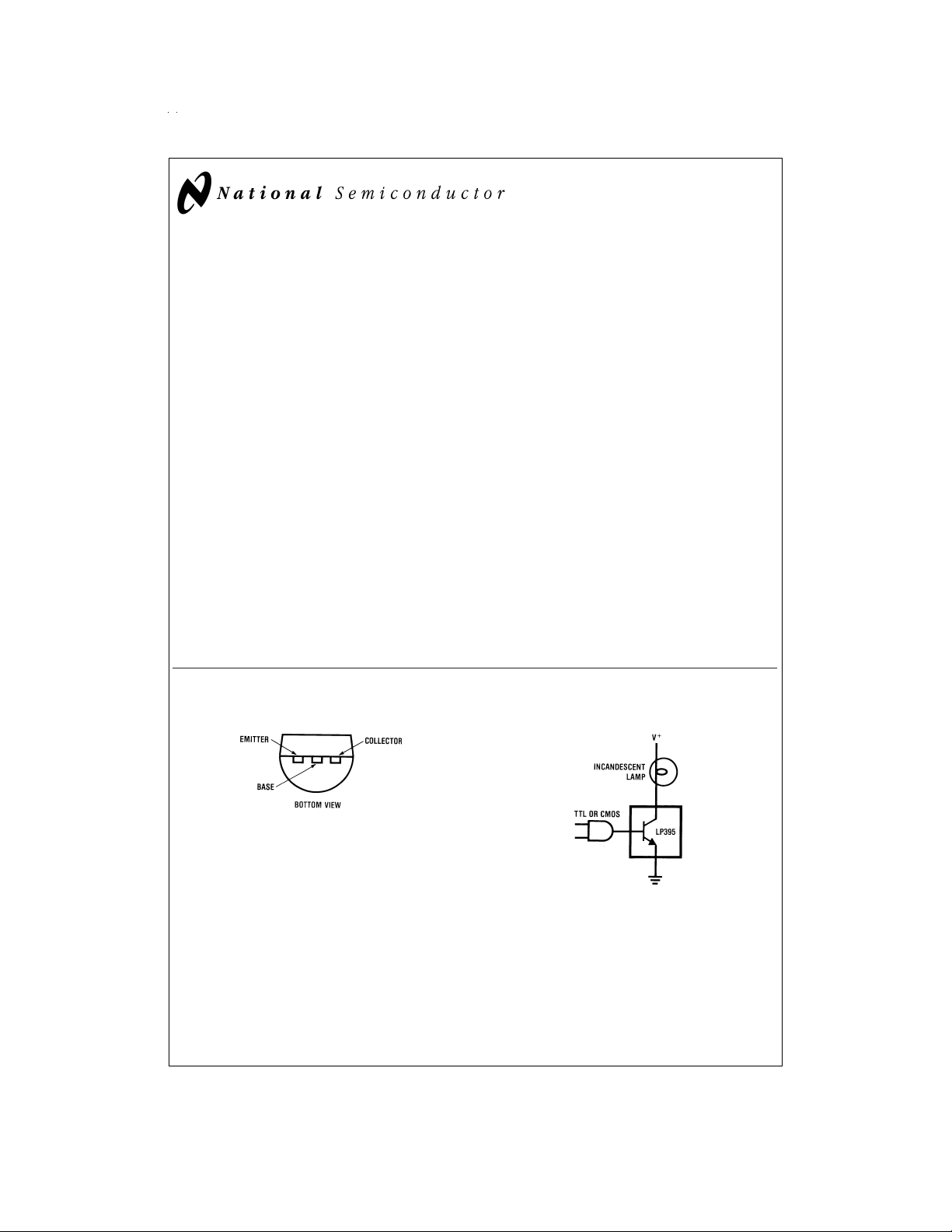
Connection Diagram Typical Applications
TO-92 Package
DS005525-1
Order Number LP395Z
See NS Package Z03A
© 1999 National Semiconductor Corporation DS005525 www.national.com
Fully Protected Lamp Driver
DS005525-3
Page 2
Absolute Maximum Ratings (Note 1)
Collector to Emitter Voltage 36V
Collector to Base Voltage 36V
Base to Emitter Voltage (Forward) 36V
Base to Emitter Voltage (Reverse) 10V
Collector Current Limit Internally Limited
Power Dissipation Internally Limited
Operating Temperature Range −40˚C to +125˚C
Storage Temperature Range −65˚C to +150˚C
Lead Temp. (Soldering, 10 seconds) 260˚C
Base to Emitter Current (Reverse) 20 mA
Electrical Characteristics
Tested Design Units
Symbol Parameter Conditions Typical Limit Limit (Limit)
(Note 3) (Note 4)
V
CE
I
CL
I
B
I
Q
V
CE(SAT)
BV
BE
V
BE
t
S
θ
JA
Note 1: AbsoluteMaximum Ratings indicate limits beyond which damage to the device may occur. Operating Ratings indicate conditions for which the device is functional, but do not guarantee specific performance limits.
Note 2: Parameters identified with boldface type apply at temp. extremes. All other numbers, unless noted apply at +25˚C.
Note 3: Guaranteed and 100%production tested.
Note 4: Guaranteed (but not 100%production tested) over the operating temperature and supply voltage ranges. These limits are not used to calculate outgoing
quality levels.
Note 5: These numbers apply for pulse testing with a low duty cycle.
Note 6: Base positive with respect to emitter.
Collector to Emitter 0.5 mA ≤ IC≤ 100 mA 36 36 V(Max)
Operating Voltage (Note 2)
Collector Current Limit V
(Note 5) V
=
BE
=
BE
=
V
BE
2V, V
CE
2V, V
CE
2V, 2V ≤ V
=
36V 45 25 20 mA(Min)
=
15V 90 60 50 mA(Min)
≤ 6V 130 100 100 mA(Min)
CE
Base Current 0 ≤ IC≤ 100 mA −0.3 −2.0 −2.5 µA(Max)
Quiescent Current V
Saturation Voltage V
Base to Emitter Break- 0 ≤ VCE≤ 36V, I
BE
BE
=
0V, 0 ≤ V
=
2V, I
≤ 36V 0.24 0.50 0.60 mA(Max)
CE
=
100 mA 1.82 2.00 2.10 V(Max)
C
=
2µA 36 36 V(Min)
B
down Voltage (Note 5)
Base to Emitter Voltage I
(Note 6) I
Switching Time V
=
5 mA 0.69 0.79 0.90 V(Max)
C
=
100 mA (Note 5) 1.02 1.40 V (Max)
C
=
CE
=
V
BE
=
20V, R
L
0V, +2V, 0V
200Ω 2µs
Thermal Resistance 0.4" leads soldered to 150 180 ˚C/W
Junction to Ambient printed circuit board (Max)
0.125" leads soldered to 130 160 ˚C/W
printed circuit board (Max)
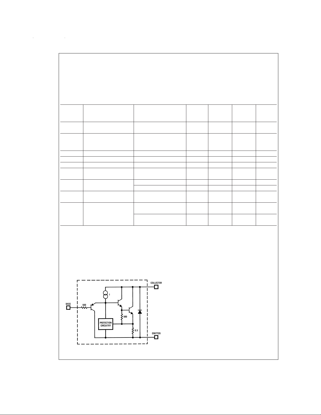
Simplified Circuit Applications Information
One failure mode incandescent lamps may experience is
one in which the filament resistance drops to a very low
value before it actually blows out. This is especially rough on
most solid-state lamp drivers and in most cases a lamp failure of this type will also cause the lamp driver to fail. Because of its high gain and blowout-proof design, the LP395 is
an ideal candidate for reliably driving small incandescent
lamps. Additionally, the current limiting characteristics of the
LP395 are advantageous as it serves to limit the cold filament inrush current, thus increasing lamp life.
DS005525-5
www.national.com 2
Page 3

Typical Performance Characteristics
5 Volt Transfer Function
Available Collector Current
Collector Current Threshold
DS005525-10
DS005525-13
36 Volt Transfer Function
Quiescent Collector Current
DS005525-11
DS005525-14
Collector Characteristics
DS005525-12
Saturation Voltage
DS005525-15
DS005525-9
www.national.com3
Page 4

Typical Applications
Lamp Flasher
(Short Circuit Proof)
Two Terminal
Current Limiter
DS005525-8
DS005525-6
Optically Isolated
Switch
DS005525-7
Composite PNP
DS005525-2
www.national.com 4
Page 5

Physical Dimensions inches (millimeters) unless otherwise noted
Order Number LP395Z
NS Package Z03A
LP395 Ultra Reliable Power Transistor
LIFE SUPPORT POLICY
NATIONAL’S PRODUCTS ARE NOT AUTHORIZED FOR USE AS CRITICAL COMPONENTS IN LIFE SUPPORT
DEVICES OR SYSTEMS WITHOUT THE EXPRESS WRITTEN APPROVAL OF THE PRESIDENT AND GENERAL
COUNSEL OF NATIONAL SEMICONDUCTOR CORPORATION. As used herein:
1. Life support devices or systems are devices or
systems which, (a) are intended for surgical implant
into the body, or (b) support or sustain life, and
whose failure to perform when properly used in
accordance with instructions for use provided in the
2. A critical component is any component of a life
support device or system whose failure to perform
can be reasonably expected to cause the failure of
the life support device or system, or to affect its
safety or effectiveness.
labeling, can be reasonably expected to result in a
significant injury to the user.
National Semiconductor
Corporation
Americas
Tel: 1-800-272-9959
Fax: 1-800-737-7018
Email: support@nsc.com
www.national.com
National does not assume any responsibility for use of any circuitry described, no circuit patent licenses are implied and National reserves the right at any time without notice to change said circuitry and specifications.
National Semiconductor
Europe
Fax: +49 (0) 1 80-530 85 86
Email: europe.support@nsc.com
Deutsch Tel: +49 (0) 1 80-530 85 85
English Tel: +49 (0) 1 80-532 78 32
Français Tel: +49 (0) 1 80-532 93 58
Italiano Tel: +49 (0) 1 80-534 16 80
National Semiconductor
Asia Pacific Customer
Response Group
Tel: 65-2544466
Fax: 65-2504466
Email: sea.support@nsc.com
National Semiconductor
Japan Ltd.
Tel: 81-3-5639-7560
Fax: 81-3-5639-7507
 Loading...