

Page 1
LP3927
Cellular/PCS System Power Management IC
LP3927 Cellular/PCS System Power Management IC
August 2002
General Description
The LP3927 system power management IC is designed for
cellular/PCS handsets as well as other portable systems that
require intelligent power management. Each device contains
five low-dropout linear regulators (LDO’s), a reset timer, a
power-up control logic, a general-purpose open drain output
that can be used to light LEDs, and a CMOS rail-to-rail
input/output operational amplifier.
Each linear regulator features an extremely low dropout
voltage of 100 mV (typ) at maximum output current. LDO1
and LDO2 are powered on and off by either the KYBD or the
VEXT pin. LDO3, LDO4 and LDO5 each have its independent enable pin. LDO1 and LDO4 are rated at 150 mA each,
LDO2 and LDO5 are rated at 200 mA each and LDO3 is
rated at 100 mA. All LDO’s are optimized for low noise and
high isolation.
The open drain output current sink can be programmed up to
150 mA by using an external low cost resistor.
A single supply, low voltage operational amplifier has rail to
rail input and output with 600 kHz of gain-bandwidth product.
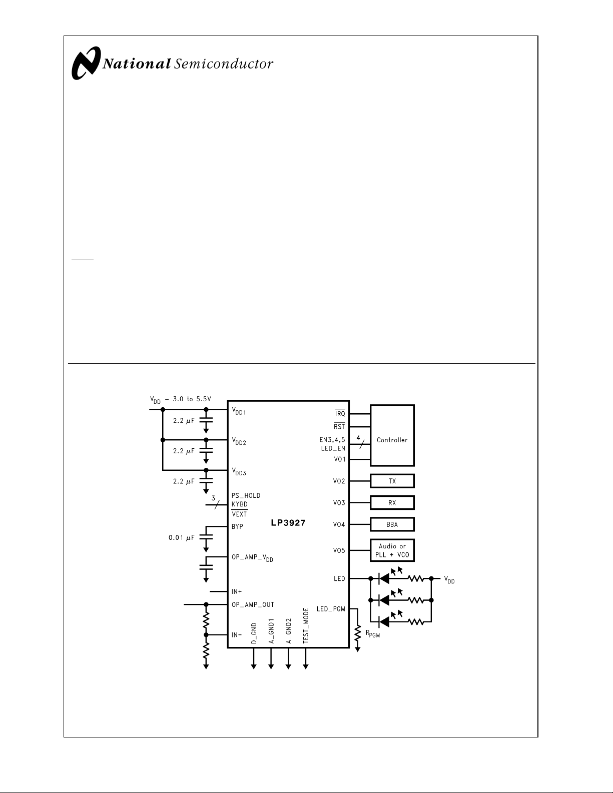
Typical Application Circuit
Key Specifications
n 3.0V to 5.5V Input Voltage Range
n Two 200 mA, Two 150 mA and One 100 mA LDO’s
n 100 mV typ Dropout Voltage
n 150 mA General-Purpose Open-drain programmable
current sink for back light LED
n Low Voltage Rail to Rail Input/Output Operational
Amplifier
n 28 pin LLP package
@
I
MAX
Applications
n Cellular/PCS handsets
n PDA’s, Palmtops, and portable terminals
n Single–Cell Li+ Systems
n 2- or 3- Cell NiMH, NiCd or Alkaline System
20037901
V
DD1,VDD2
© 2002 National Semiconductor Corporation DS200379 www.national.com
and V
must be tied together externally. Collectively called VDD.
DD3
Page 2
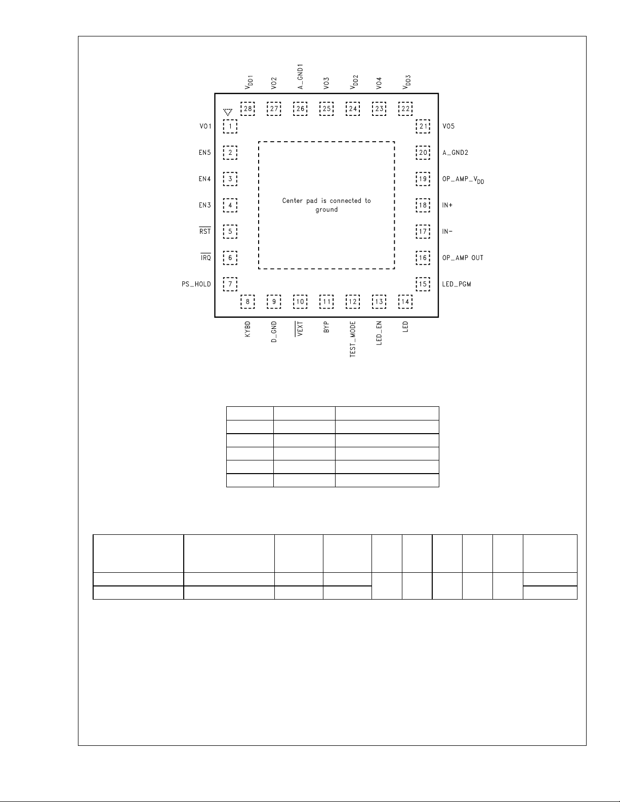
LP3927 Pin Out Diagram (Top View)
LP3927
20037902
Output Current Rating and Voltage Options
I
(mA) Voltage Options (V)
MAX
LDO1 150 1.8, 1.9, 2.5, 2.6*, 2.7
LDO2 200 1.8, 2.85*, 2.9, 3.0
LDO3 100 2.7, 2.8, 2.9
LDO4 150 2.7, 2.8, 2.9
LDO5 200 2.7, 2.8, 2.9, 3.0
*
denotes the voltage options that are available currently. For other options, please contact the
National Semiconductor factory sales office/distributors for availability and specifications.
*
, 3.0
*
, 3.0
*
Ordering Information
LP3927 Supplied as
1000 Units, tape and
reel
LP3927ILQ-AH LP3927ILQX-AH X
LP3927ILQ-AJ LP3927ILQX-AJ X 3927AJ
For LDO delay options, please refer to Electrical Characteristics Table.
LP3927 Supplied as
4500 Units, tape and
reel
Standard
LDO delay
Optional
LDO delay
VO1
VO2
VO3
VO4
VO5
(V)
(V)
(V)
2.6 2.85 2.9 2.9 3.0
(V)
(V)
TOP
MARKING
3927AH
www.national.com 2
Page 3
Pin Description
Pin Name Functional Description
1 VO1 150 mA, LDO1 output pin.
2 EN5 LDO5 enable input.
3 EN4 LDO4 enable input.
4 EN3 LDO3 enable input.
5 RST
6 IRQ
7 PS_HOLD Input from the processor to the LP3927. A HIGH indicates a steady supply of power is
8 KYBD An active high input signal indicating the keyboard “On/Off” button has been asserted. Refer
9 D_GND Digital ground, used primarily for the digital and DAC circuits.
10 VEXT
11 BYP Reference bypass pin.
12 TEST_MODE Pin used for production testing, factory use only. This pin should be grounded in applications.
13 LED_EN LED driver enable input.
14 LED LED driver, drain connection of the LED drive MOSFET.
15 LED_PGM LED drive current programming pin.
16 OP_AMP_OUT Operational amplifier output pin.
17 IN− − input of the Op-Amp.
18 IN+ + input of the Op-Amp.
19 OP_AMP_V
20 A_GND2 Ground for analog.
21 VO5 200 mA, LDO5 output pin.
22 V
DD3
23 VO4 150 mA, LDO4 output pin.
24 V
DD2
25 VO3 100 mA, LDO3 output pin.
26 A_GND1 Ground for analog.
27 VO2 200 mA, LDO2 output pin.
28 V
DD1
Externally pulled high, open drain output to processor/memory reset.
Externally pulled high, open drain output to processor interrupt indicating KYBD has gone
high.
granted. Refer to ’Application Hints’ section for more detail.
to ’Application Hints’ section for more detail.
Active low input indicating a battery charger insertion Refer to ’Application Hints’ section for
more detail.
Power supply pin for Op-Amp.
DD
Input power pin for LDO5. V
DD1,VDD2
Input power pin for LDO3 and LDO4. V
Input power pin for LDO1 and LDO2. V
and V
DD3
DD1,VDD2
DD1,VDD2
must be tied together externally.
and V
and V
must be tied together externally.
DD3
must be tied together externally.
DD3
LP3927
www.national.com3
Page 4
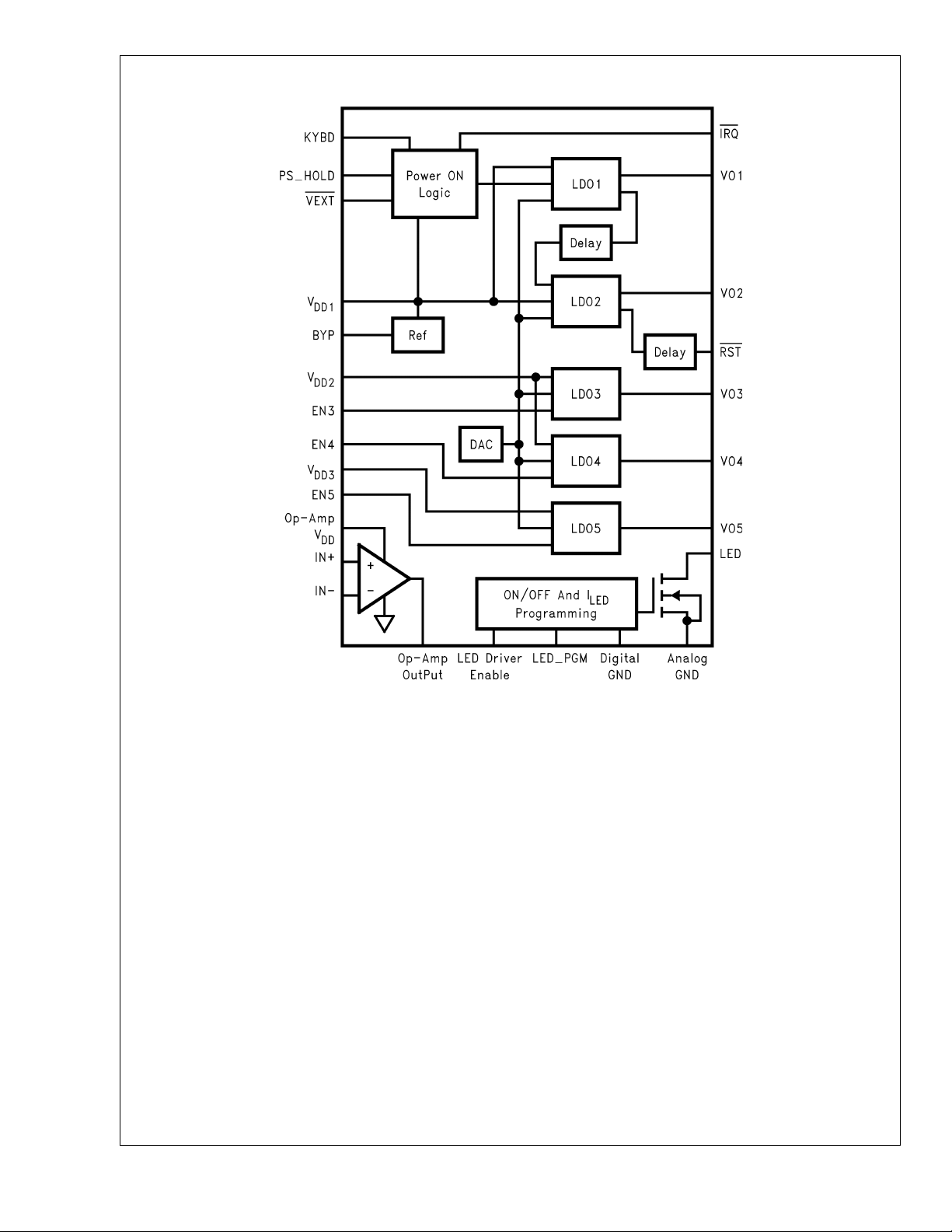
Functional Block Diagram
LP3927
20037903
www.national.com 4
Page 5
LP3927
Absolute Maximum Ratings (Notes 1,
All other pins 2 kV
2)
If Military/Aerospace specified devices are required,
please contact the National Semiconductor Sales Office/
Distributors for availability and specifications.
All pins except LED_PGM,
BYP, op amp’s inputs & output −0.3V to 6.0V
OP_AMP_OUT, IN-, IN+ -0.3V to 5.5V
GND to GND SLUG
±
0.3V
Junction Temperature 150˚C
Storage Information −65˚C to 150˚C
Soldering Temperature
Pad Temperature 235˚C
Maximum Power Dissipation (Note 3) 2.6W
Operating Ratings (Notes 1, 2)
V
DD1,VDD2,VDD3
EN3, EN4, EN5 −0.3V to (V
C
:
OUT
Capacitance 1.0 µF to 20.0 µF
ESR 0.005Ω to 0.5Ω
Junction Temperature −40˚C to 125˚C
Operating Temperature −40˚C to 85˚C
Thermal Resistance (Note 5)
θ
(LLP28) 30.8˚C/W
JA
Maximum Power Dissipation (Note 6) 1.78W
, KYBD, OP_AMP_V
ESD (Note 4):
KYBD 4 kV
Electrical Characteristics, LDO’s
Unless otherwise noted, VDD=V
OUT(target)
0.1 µF. Typical values and limits appearing in normal type apply for T
the entire junction temperature range for operation, −40˚C to +85˚C. (Notes 7, 8)
Symbol Parameter Conditions Typical
V
∆V
DD
OUT
Input Voltage Range V
Output Voltage Tolerance I
Load Regulation I
Line Regulation V
Total Accuracy Error −3.5 +3.5 %
V
IN-VOUT
e
N
Dropout Voltage I
Output Noise Voltage I
PSRR Power Supply Ripple
Rejection Ratio
Cross Talk (Note 10) 30 dB
I
I
I
C
R
Q
GND
SC
OUT
SHUNT
Quiescent Current I
Ground Current I
Short Circuit Current Limit V
Output Capacitor Capacitance 120 µF
VO2-VO5Output Shunt
Resistor
+ 0.7V, CIN(V
DD1,VDD2,VDD3
OUT=IMAX
V
DD
OUT
V
DD
DD=VOUT(target)
I
OUT=IMAX
OUT=IMAX
OUT
/2,
= 3.7V
= 100 µA to I
= 3.7V
/2
= 100 µA,
DD1,VDD2,VDD3
,KYBD 3.7 3 5.5 V
,
MAX
+0.7V to 5.5V
(Note 9) 100 170
) = 4.7 µF, C
= 25˚C. Limits appearing in boldface type apply over
J
OUT
10 Hz ≤ f ≤ 100 kHz 27 µV
CIN= 2.2µF, I
OUT=IMAX
,
f = 100 Hz
f=1kHz
f=10kHz
f = 100 kHz
= 0, PS_HOLD = KYBD = 0
OUT
VEXT = V
OUT1=IOUT2
DD
= 1 mA,
LDO3, LDO4, LDO5 OFF
I
OUT1,IOUT2,IOUT3,IOUT4,IOUT5=IMAX
=0V 400 %ofI
OUT
ESR 5 500 mΩ
3.0V to 5.5V
DD
+ 0.3V)
DD
(VO1 to VO5) = 2.2 µF, C
Limit
Min Max
byp
Units
−2 +2 %
−2 +2 %
−40 +40 mV
mV
200
45
45
dB
30
10
5
µA
8
100 200 µA
400 950
70 200 Ω
=
rms
MAX
www.national.com5
Page 6

Electrical Characteristics, Digital Interface
LP3927
Symbol Parameter Conditions Typical
V
OL
V
IH
V
IL
I
LEAKAGE
Logic Low Output RST and IRQ
I
= 250 µA
LOAD
Logic High Input KYBD and VEXT 0.7 V
EN3–5, PS_HOLD 1.4
LED_EN 0.85V
Logic Low Input KYBD and VEXT 0.2 V
EN3–5, PS_HOLD 0.4
LED_EN 0.2 V
Input Leakage Current VEXT, PS_HOLD, IRQ,
KYBD, EN3– 5, 0V ≤ VDD≤ 5.5V
Electrical Characteristics, Error Flag
Symbol Parameter Conditions Typical
V
Th-H
V
Th-L
t
DELAY-H
t
DELAY-L
R
DELAY
t
DELAY
t
Hold-UP
Error Flag High Vo1and Vo2Outputs (Note 11) 95 92 98 % V
Error Flag Low 90 89 92
(Note 12) 6 0 10 µs
Keyboard Debounce Delay (Note 13) 32 16 64 ms
VEXT Debounce Delay
(Note 13) 32 16 64 ms
RST Reset Delay (Note 14) 20 10 40 ms
LDO Delay, standard (Note 15) 125 0 250 µs
LDO Delay, optional 10 5 20 ms
PS_HOLD Input (Note 16) 500 250 1000 ms
Limit
Min Max
Units
150 mV
DD
DD
DD
DD
−10 +10 µA
Limit
Min Max
Units
6 0 10 µs
V
V
OUT
Electrical Characteristics, Backlight LED Driver
Symbol Parameter Conditions Typical
I
LED
Drive Current V
LED
= 1V, R
= 130kΩ 150 125 175 mA
PGM
Electrical Characteristics, Operational Amplifier
Unless otherwise noted, V
OP_AMP_VDD
appearing in normal type apply for T
= 3.3V, VCM=V
= 25˚C. Limits appearing in boldface type apply over the entire junction temperature
J
OUT=VOP_AMP_VDD
/2 and R
range for operation, −40˚C to +85˚C. (Note 7)
Symbol Parameter Conditions Typical
V
DD
V
OS
TC V
I
B
I
OS
R
IN
CMRR Common-Mode Rejection Ratio 0V ≤ V
PSRR Power Supply Rejection Ratio V
OP_AMP_V
DD
Input Offset Voltage 1.2 10 mV
Offset Voltage Drift 10 µV/˚C
OS
Input Bias Current 0.2 nA
Input Offset Current 0.1 nA
Input Resistance
≤ 2.7V 70 dB
CM
OP_AMP_VDD
= 2.7V to
3.3V
=0
,V
CM
C
IN
Common-Mode Input Capacitor 3 pF
>
LOAD
1MΩ. Typical values and limits
3.3 3 5.5 V
>
60 dB
Limit
Min Max
Limit
Min Max
Units
Units
1GΩ
www.national.com 6
Page 7

Electrical Characteristics, Operational Amplifier (Continued)
Unless otherwise noted, V
OP_AMP_VDD
appearing in normal type apply for T
= 3.3V, VCM=V
= 25˚C. Limits appearing in boldface type apply over the entire junction temperature
J
OUT=VOP_AMP_VDD
/2 and R
range for operation, −40˚C to +85˚C. (Note 7)
Symbol Parameter Conditions Typical
V
OUT
I
S
Output Swing R
Supply Current V
=2kΩ 0.5 V
LOAD
OP_AMP_VDD
= 3.0V 0.5 1.4 mA
SR Slew Rate 0.7 V/µs
GBW Gain-Bandwidth Product 0.6 MHz
Note 1: Absolute Maximum Ratings are limits beyond which damage to the device may occur. Operating Ratings are conditions under which operation of the device
is guaranteed. Operating Ratings do not imply guaranteed performance limits. For guaranteed performance limits and associated test conditions, see the Electrical
Characteristics tables.
Note 2: All voltages are with respect to the potential at the GND pin.
Note 3: The Absolute Maximum power dissipation depends on the ambient temperature and can be calculated using the formula
P=(TJ−TA)/θJA, (1)
where TJis the junction temperature, TAis the ambient temperature, and θJAis the junction-to-ambient thermal resistance. The 2.6W rating appearing under
Absolute Maximum Ratings results from substituting the Absolute Maximum junction temperature, 150˚C, for T
be dissipated safely at ambient temperatures below 70˚C. Less power can be dissipated safely at ambient temperatures above 70˚C. The Absolute Maximum power
dissipation can be increased by 32.5 mW for each degree below 70˚C, and it must be derated by 32.5 mW for each degree above 70˚C.
Note 4: The human-body model is used. The human-body model is 100 pF discharged through 1.5 kΩ.
Note 5: This figure is taken from a thermal modeling result. The test board is a 4 layer FR-4 board measuring 101mm x 101mm x 1.6mm with a3x3array of thermal
vias. The ground plane on the board is 50mm x 50mm. Ambient temperature in simulation is 22˚C, still air. Power dissipation is 1W.
Note 6: Like the Absolute Maximum power dissipation, the maximum power dissipation for operation depends on the ambient temperature. The 1.78W rating
appearing under Operating Ratings results from substituting the maximum junction temperature for operation, 125˚C, for T
(1) above. More power can be dissipated at ambient temperatures below 70˚C. Less power can be dissipated at ambient temperatures above 70˚C. The maximum
power dissipation for operation can be increased by 32.5 mW for each degree below 70˚C, and it must be derated by 32.5 mW for each degree above 70˚C.
Note 7: All limits guaranteed at room temperature (standard typeface) and at temperature extremes (bold typeface). All room temperature limits are 100%
production tested or guaranteed through statistical analysis. All limits at temperature extremes are guaranteed via correlation using standard Statistical Quality
Control (SQC) methods.
Note 8: The target output voltage, which is labeled V
Note 9: Dropout voltage is the input-to-output voltage difference at which the output voltage is 100 mV below its nominal value. This specification does not apply
in cases it implies operation with an input voltage below the 2.5V minimum appearing under Operating Ratings. For example, this specification does not apply for
devices having 1.5V outputs because the specification would imply operation with an input voltage at or about 1.5V.
Note 10: Pulsing the load of LDO X from 100µA to Imax and measuring its effects at the output of LDO Y. LDO Y enabled but under no load.
Note 11: The error flags are internal to the chip. There is no external access to the signals. LDO1 error flag and the LDO2 error flag will go HIGH when the respective
LDO reaches its V
Note 12: The t
its error flag going LOW. Same delays apply to LDO2 and its error flag.
Note 13: Refer to Timing Diagram.
Note 14: The delay between LDO2 error flag HIGH and RST signal HIGH in the power up sequence. In the power down sequence, it is the delay between RST
signal LOW and LDO2 disabled.
Note 15: The delay between LDO1 error flag HIGH and LDO2 enable in power up sequence. In the power down sequence, it is the delay between LDO2 error flag
LOW and LDO1 disable. For the optional LDO delay, please contact the factory for availability.
Note 16: Time between RST high and PS_HOLD going high.
value. The error flags will go LOW when the respective LDO reaches its V
Th-H
is the delay between LDO1 reaching its V
DELAY-H
, is the desired or ideal output voltage.
OUT(target)
and its error flag going HIGH. The t
Th-H
Th-L
value.
DELAY-L
>
1MΩ. Typical values and limits
LOAD
Limit
Min Max
Units
3.1
, 70˚C for TA, and 30.8˚C/W for θJA. More power can
J
, 70˚C for TA, and 30.8˚C/W for θJAinto
J
is the delay between LDO1 reaching its V
Th-L
and
LP3927
www.national.com7
Page 8

Typical Performance Characteristics Unless otherwise specified, C
0.01 µF, V
LP3927
DD=VOUT
LDO4 Enable Response (Cout=2.2µF) LDO5 Enable Response (Cout=2.2µF)
+ 0.2V, TA= 25˚C, Enable pin is tied to VDD.
PSRR vs Frequency LDO3 Enable Response (Cout=2.2µF)
20037908
= 1 µF ceramic, C
IN
20037909
BYP
=
20037910 20037911
LDO2 (1.8V Option) Load Transient LDO2 (2.85V Option) Load Transient
20037929 20037930
www.national.com 8
Page 9

LP3927
Typical Performance Characteristics Unless otherwise specified, C
0.01 µF, V
DD=VOUT
LDO4 (2.8V Option) Load Transient LDO5 (3.0V Option) Load Transient
LDO2 (1.8V Option) Line Transient LDO2 (2.85V Option) Line Transient
+ 0.2V, TA= 25˚C, Enable pin is tied to VDD. (Continued)
20037931 20037932
= 1 µF ceramic, C
IN
BYP
=
20037933 20037934
LDO4 (2.8V Option) Line Transient LDO5 (3.0V Option) Line Transient
20037935 20037936
www.national.com9
Page 10

LP3927
Keyboard Start-Up/Shut-Down
Note: Diagram indicates Open Drain IRQ tied to VDD.
***
= Internal signal
1. Keyboard de-bounce delay, 32 msec typ.
2. Delay between LDO1 reaching 95% of its output voltage and LDO2 enable, 125 µsec typical.
3. Both LDO1 and LDO2 outputs reach 95% of respective output voltage, start RST timer.
4. RST delay, 20 msec typical.
5. IRQ is active low.
6. Keyboard press must be greater than 32 msec.
7. PS_HOLD timer begins upon RST going high.
8. Maximum of 500 msec period from RST going high to PS_HOLD going high.
9. Response time from PS_HOLD going low to RST going low.
10. Delay between RST high-low transition to LDO2 disable.
11. Delay between LDO2 disable and LDO1 disable.
20037925
www.national.com 10
Page 11

Keyboard Held at Start-Up/Shut-Down
LP3927
Note: Diagram indicates Open Drain IRQ tied to VDD.
***
= Internal signal
1. Keyboard de-bounce delay, 32msec typ.
2. Delay between LDO1 reaching 95% of its output voltage and LDO2 enable.
3. Both LDO1 and LDO2 outputs reach 95% of the respective output voltage, start RST timer.
4. Reset delay.
5. IRQ is active low.
6. Keyboard press must be greater than 32 msec.
7. PS_HOLD timer begins upon RST going high.
8. Maximum of 500 msec period from RST going high to PS_HOLD going high.
9. Response time from PS_HOLD going low to RST going low.
10. Delay between RST high-low transition to LDO2 disable.
11. Delay between LDO2 disable and LDO1 disable.
20037926
www.national.com11
Page 12

LP3927
VEXT Detect Start-Up/Shut Down
Note: Diagram indicates Open Drain IRQ tied to VDD.
***
= Internal signal
1. VEXT goes active low.
2. VEXT 32 msec de-bounce period.
3. Delay between LDO1 and LDO2 enables.
4. Both LDO1 and LDO2 outputs reach 95% of respective output voltage, start Reset timer.
5. Reset delay.
6. Period between Reset and PS_HOLD going high is not relevant since VEXT is low
7. PS_HOLD goes low but LDOs continue to run since VEXT is low.
8. PS_HOLD is low and VEXT goes high, RST pin goes low.
9. Delay between RST going low and LDO2 disabled.
10. Delay between LDO2 and LDO1 disabled.
20037927
www.national.com 12
Page 13

VEXT Detect W/Keyboard Interrupts
LP3927
Note: Diagram indicates Open Drain IRQ tied to VDD.
***
= Internal signal
1. VEXT goes active low.
2. VEXT 32 msec de-bounce period.
3. Delay between LDO1 and LDO2 enable.
4. Both LDO1 and LDO2 outputs reach 95% of respective output voltage, start Reset timer.
5. Reset delay.
6. Keyboard de-bounce delay.
7. Keyboard pulse must be a minimum of 32 msec.
8. PS_HOLD may go low after Key press, but LDOs stay on since VEXT is low.
9. VEXT goes high, begin shutdown since PS_HOLD is low.
10. Delay between RST going low and LDO2 disabled.
11. Delay between LDO2 disable and LDO1 disabled.
20037928
www.national.com13
Page 14

Application Hints
LP3927
LP3927 Function Description
The LP3927 is designed for cellular/PCS handsets. The
LDOs power the microprocessor, RF and digital sections of
the phone. When a KYBD debounce of longer than 32 ms is
detected by the LP3927, the IRQ signal is asserted and sent
to the microprocessor. In addition, the KYBD signal turns on
LDO1. When LDO1 reaches 95% of its output voltage option, a 125 µs delay (standard LDO delay. The optional LDO
delay has a 10msec delay) takes place, and LDO2 turns on.
When LDO2 reaches 95% of its output voltage option, RST
goes high after a 20 ms delay. At this point, the microprocessor comes out of reset and the LP3927 starts the PS_HOLD timer. If PS_HOLD goes high before 500 ms, IRQ is
de-asserted. If PS_HOLD stays low for longer than 500 ms,
IRQ will still de-assert, but RST will also be asserted, and the
part will power down.
The power down sequence is the exact reverse of the power
up sequence. PS_HOLD from the microprocessor goes low,
indicating a request to turn the part off. This causes RST to
go low. LDO2 will be turned off after a 20 ms delay. When
LDO2 drops to 90% of its output voltage option, LDO1 will
start to turn off after a 125 µs (or a 10msec) delay. Another
KYBD debounce after power up does not necessary mean
power down.
Whenever LDO1 or LDO2 falls under 90% of the output
voltage option, RST immediately goes low to bring
PS_HOLD low in order to turn the part off.
Plugging the charger into the cell phone will cause an external signal VEXT to toggle from high to low. The LP3927 will
respond differently to this signal depending on the scenario:
Case 1: If a charger is plugged into the cell phone after the
phone is already on, the VEXT signal go from high to low.
The LP3927 will acknowledge this signal but all other signals
remain unchanged.
Case 2: If a charger is plugged into the phone while the
phone is off, VEXT signal goes from high to low and the
LP3927 will proceed to turn LDO1 on after a 32 ms delay,
and the identical power-up sequence follows. This case
bypasses the power-up initiated by KYBD and IRQ. KYBD
remains low and IRQ remains high at all time during
power-up.
When the charger is plugged in, the phone cannot be turned
off unless both VEXT goes high and PS_HOLD goes low.
LDOs
The LP3927 contains five LDOs. LDO1 and 2 are powered
by the V
and LDO5 is powered by the V
must be tied together externally. All five LDOs accept an
input voltage from 3.0V to 5.5V. This accommodates the full
usable range of a single Li-On battery.
LDO1 and 4 each provide 150 mA of current. LDO2 and 5
each provide 200 mA of current. LDO3 provides 100 mA of
current. The output of each LDO can be programmed to
different voltage levels at the factory. Refer to “Output Current Rating and Voltage Options” Table for more details.
LDO Input Capacitor
An input capacitance of ≈ 2.2 µF is required between each
V
DD
may be increased without limit).
line; LDO3 and 4 are powered by the V
DD1
DD3
line. V
DD1,VDD2
input pins and ground. (The amount of the capacitance
DD2
and V
line;
DD3
This capacitor must be located a distance of not more than
1 cm from the input pin and returned to a clean analog
ground. Any good quality ceramic, tantalum, or film capacitor
may be used at the inputs.
Important: Tantalum capacitors can suffer catastrophic failures due to surge current when connected to a
low-impedance source of power (like a battery or a very
large capacitor). If a tantalum capacitor is used at the input,
it must be guaranteed by the manufacturer to have a surge
current rating sufficient for the application.
There are no requirements for the ESR on the input capacitor, but tolerance and termperature coefficient must be considered when selecting the capacitor to ensure the capacitance will be ≈ 1 µF over the entire operating temperature
range.
LDO Output Capacitor
The LDOs are designed specifically to work with very small
ceramic output capacitors. A ceramic capacitor (X7R, X5R,
Z5U, or Y5V) in 1 µF to 20 µF range with 5 mΩ to 500 mΩ
ESR range is suitable in the LP3927 application circuit.
It may also be possible to use tantalum or film capacitors at
the output, but these are not as attractive for reasons of size
and cost.
The output capacitor must meet the requirement for minimum amount of capacitance and also have an ESR (Equivalent Series Resistance) value which is within a stable range
(5 mΩ to 500 mΩ).
LED Current Driver
The LED pin on the LP3927 is an open-drain output that can
provide up to 150 mA to drive backlight LEDs. It is turned on
when the LED_EN pin is pulled high, and off when the
LED_EN pin is pulled low. The external resistor R
PGM
connected to the LED_PGM pin programs the output current of
LED. A 130 kΩ resistor sets the output current to 150 mA. An
approximated equation between R
PGM
and I
LED
is:
Operational Amplifier
The LP3927 has an internal op amp with rail-to-rail input and
output and a 600 kHz of gain-bandwidth product.
Leadless Leadframe Package (LLP)
The LP3927 is packaged in a 28-lead LLP package for
enhanced thermal performance. The 28-lead LLP measures
5mmx5mmx0.75 mm. Its small size and low profile is
ideal for handset applications and other portable applications
that require power management.
Thermal Performance
The LLP package is designed for enhanced thermal performance because of the exposed die attach pad at the bottom
center of the package. It brings advantage to thermal performance by creating a very direct path for thermal dissipation.
Compared to the traditional leaded packages where the die
attach pad is embedded inside the mold compound, the LLP
reduces a layer in the thermal path.
The thermal advantage of the LLP package is fully realized
only when the exposed die attach pad is soldered down to a
thermal land on the PCB board and thermal vias are planted
underneath the thermal land. Based on a LLP thermal mea-
www.national.com 14
Page 15

LP3927
Application Hints (Continued)
surement, junction to ambient thermal resistance (θ
be improved by as much as two times if a LLP is soldered on
the board with thermal land and thermal vias than if not.
Consider the following equation:
Where P is the power dissipated, TJis the maximum junction
temperature of the die, T
is the thermal resistance of the package. TJis specified
θ
JA
is the ambient temperature, and
A
at 150˚C.
According to the above equation, in the case where the
LP3927 is dissipating 3W of power, T
when T
of 125˚C and θJAof 30.8˚C/W are used in the
J
is limited to 32.6˚C
A
equation. In order to operate at a higher ambient temperature, power dissipation has to be reduced. A curve of maximum power dissipation vs ambient temperature is provided
below.
Power Dissipation vs Ambient Temperature
=30.8˚C/W)
(θ
JA
JA
) can
Layout Consideration
The LP3927 has an exposed die attach pad located at the
bottom center of the LLP package. It is imperative to create
a thermal land on the PCB board when designing a PCB
layout for the LLP package. The thermal land helps to conduct heat away from the die, and the land should be the
same dimension as the exposed pad on the bottom of the
LLP (1:1 ratio). The land should be on both the top and the
bottom layer of the PCB board. In addition, thermal vias
should be added inside the thermal land to conduct more
heat away from the surface of the PCB to the ground plane.
Typical pitch and outer diameter for these thermal vias are
1.27 mm and 0.33 mm respectively. Typical copper via barrel
plating is 1 oz. although thicker copper may be used to
improve thermal performance. The LP3927 bottom pad is
connected to ground. Therefore, the thermal land and vias
on the PCB board need to be connected to ground.
For more information on board layout techniques, refer to
Application Note 1187 “Leadless Leadframe Package
(LLP).” The application note also discusses package handling, solder stencil, and assembly process.
20037915
www.national.com15
Page 16

Physical Dimensions inches (millimeters)
unless otherwise noted
LP3927 Cellular/PCS System Power Management IC
28 Lead LLP Package
NS Package Number lqa28A
LIFE SUPPORT POLICY
NATIONAL’S PRODUCTS ARE NOT AUTHORIZED FOR USE AS CRITICAL COMPONENTS IN LIFE SUPPORT
DEVICES OR SYSTEMS WITHOUT THE EXPRESS WRITTEN APPROVAL OF THE PRESIDENT AND GENERAL
COUNSEL OF NATIONAL SEMICONDUCTOR CORPORATION. As used herein:
1. Life support devices or systems are devices or
systems which, (a) are intended for surgical implant
into the body, or (b) support or sustain life, and
whose failure to perform when properly used in
accordance with instructions for use provided in the
2. A critical component is any component of a life
support device or system whose failure to perform
can be reasonably expected to cause the failure of
the life support device or system, or to affect its
safety or effectiveness.
labeling, can be reasonably expected to result in a
significant injury to the user.
National Semiconductor
Corporation
Americas
Email: support@nsc.com
www.national.com
National Semiconductor
Europe
Fax: +49 (0) 180-530 85 86
Email: europe.support@nsc.com
Deutsch Tel: +49 (0) 69 9508 6208
English Tel: +44 (0) 870 24 0 2171
Français Tel: +33 (0) 1 41 91 8790
National Semiconductor
Asia Pacific Customer
Response Group
Tel: 65-2544466
Fax: 65-2504466
Email: ap.support@nsc.com
National Semiconductor
Japan Ltd.
Tel: 81-3-5639-7560
Fax: 81-3-5639-7507
National does not assume any responsibility for use of any circuitry described, no circuit patent licenses are implied and National reserves the right at any time without notice to change said circuitry and specifications.
 Loading...