

Page 1

PRELIMINARY
March 2007
LP3913
Power Management IC for Flash Memory Based Portable
Media Players
General Description
The LP3913 is a programmable system power management
unit that is optimized for Flash Memory based Portable Media
Players.
The LP3913 incorporates 2 low-dropout LDO voltage regulators, 3 integrated Buck DC/DC converters with Dynamic Voltage Scaling (DVS), a 4-channel 8-bit A/D converter, and a
dual source Li-Ion/polymer battery charger. The charger has
the capability to charge and maintain a single cell battery from
a regulated wall adapter or USB power. When both USB and
adapter sources are present, then the adapter source takes
precedence and switching between USB and adapter power
sources is seamless. In addition, the battery charger supports
power routing, which allows system usage immediately after
an external power source has been detected. The LP3913
also incorporates some advanced battery management functions such as battery temperature measurement, reverse current blocking for USB, LED charger status indication,
thermally regulated internal power FETs, battery voltage
monitoring, over-current protection and a 10 hour safety
timer.
The 4-channel A/D converter measures the battery voltage
and charge current, which can be used for fuel gauging. Two
undedicated channels can be used to measure other analog
parameters such as discharge current, battery temperature,
keyboard resistor scanning and more.
The various IC parameters are programmable through a
400 kHz I2C compatible interface.
The LP3913 is available in a thermally-enhanced
6x6x0.8 mm 48 LLP package and operates over an ambient
temperature range of –40°C to +85°C.
Features
■
2 low-dropout regulators -- LDO1 is used for general
purpose applications, LDO2 is used for low-noise analog
applications. Both LDOs have programmable output
voltages.
■
Green and Red LED charger status drivers
■
4-channel 8-bit dual slope a/d converter
■
3 High-efficiency DVS Buck converters
■
400 kHz I2C compatible interface
■
Linear constant-current / constant-voltage charger for
single cell lithium-ion batteries
■
USB and Adapter charging
■
System power supply management
■
6x6x0.8mm 48 LLP package
■
Voltage and thermal supervisory circuits
■
Continuous battery voltage monitoring
■
Interrupt Request output with 8 sources
■
LP3913 is pin for pin and software compatible with the
LP3910 Hard Drive based PMIC
Key Specifications
■
LDO1: 150 mA, 1.2V–3.3V
■
LDO2: 150 mA, 1.3V–3.3V
■
Buck1: 600 mA, 0.8V–2.0V
■
Buck2: 600 mA, 1.8V–3.3V
■
Buck3: 500 mA, 1.8V–3.3V
■
50 mΩ battery path resistance
■
100 mA–1000 mA full-rate charge current using wall
adapter
■
Selectable 0.05C and 0.1C EOC current
■
USB current limit of 100 mA, 500 mA, and 800 mA
■
USB pre-qual current of 50 mA
■
Selectable 4.1V, 4.2V or 4.38V battery termination
voltages
■
0.35% battery termination accuracy
■
±1 LSB INL/DNL on 8-bit a/d converter
Applications
■
Flash-based portable media players
■
Portable gaming devices
■
Portable navigation systems
© 2007 National Semiconductor Corporation 300001 www.national.com
LP3913 Power Management IC for Flash Memory Based Portable Media Players
Page 2
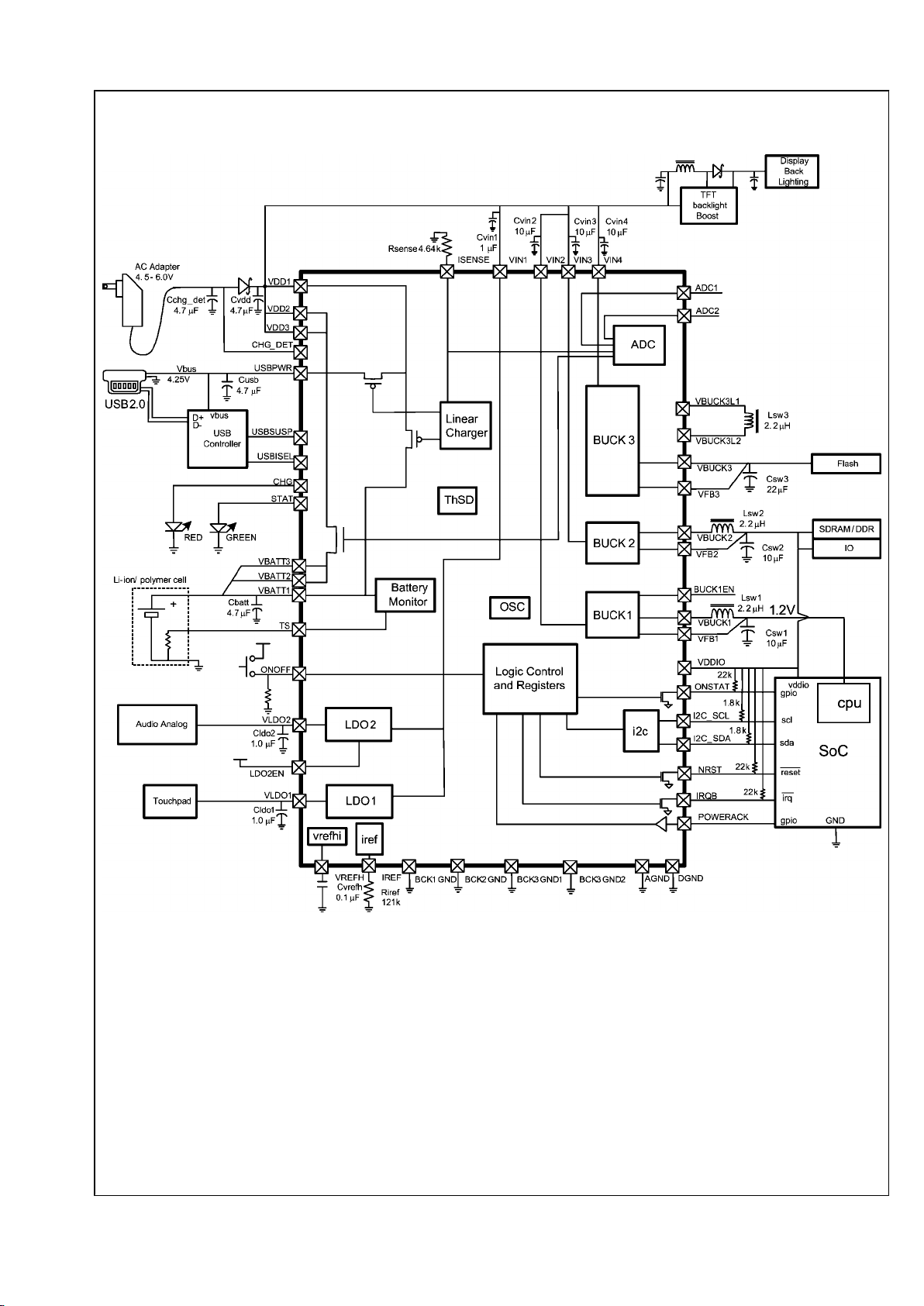
Typical Application Circuit
30000101
FIGURE 1. Application Diagram
www.national.com 2
LP3913
Page 3
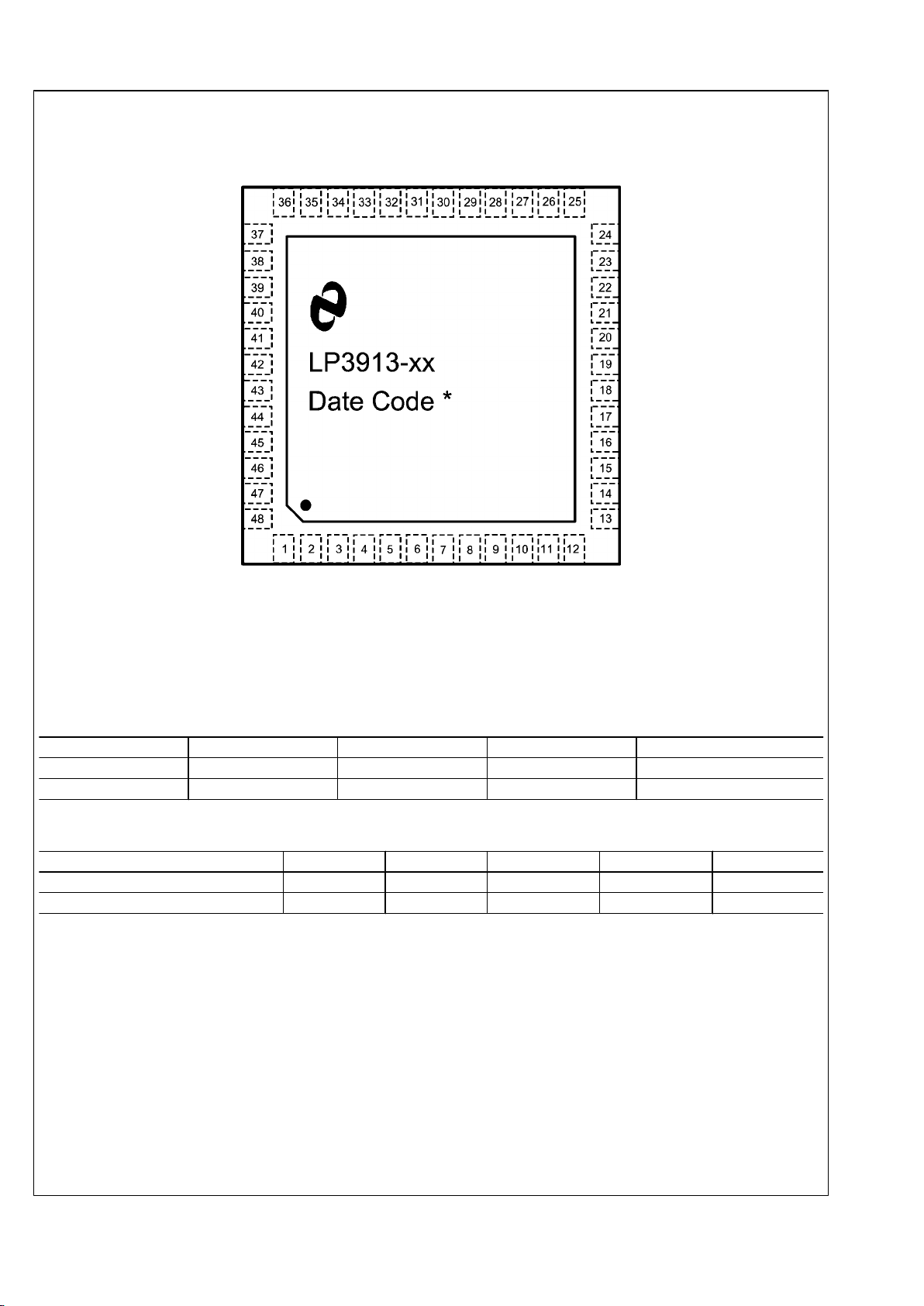
Connection Diagram
Device Connection Diagram
30000102
48 LLP Package (Top View)
SQF48A
The physical placement of the package marking will vary from
part to part.
(*) UZXYTT format: ‘U’ – wafer fab code; ‘Z’ – assembly code;
‘XY’ 2 digit date code; ‘TT’ – die run code
See http://www.national.com/quality/
marking_conventions.html for more information on marking
information.
Ordering Information
Order Number Package Type NSC Package Drawing Top Mark Supplied As
LP3913SQ-AA 48-lead LLP SQF48A LP3913SQ-AA 250 tape & reel
LP3913SQX-AA 48-lead LLP SQF48A LP3913SQX-AA 3000 tape & reel
Device Default Options
Order Number LDO1 LDO2 Buck1 Buck2 Buck3
LP3910SQ-AA 2.0V 3.3V 1.2V 3.3V 3.3V
LP3910SQX-AA 2.0V 3.3V 1.2V 3.3V 3.3V
3 www.national.com
LP3913
Page 4
Pin Descriptions
Name I/O Type Functional Description Pin #
TS I A Battery temperature sense pin. This pin is normally connected to the thermistor
pin of the battery cell.
1
VBATT1 O A Positive battery terminal. This pin must be externally shorted to VBATT2 and
VBATT3
2
AGND G G Analog Ground 3
VREFH O A Connection to bypass capacitor for internal high reference 4
LDO2EN I D Digital input to enable/disable LDO2 5
VLDO2 O A LDO2 Output 6
VIN1 I PWR Power input to LDO1 and LDO2. VIN1 pin must be externally shorted to the VDD
pins.
7
VLDO1 O A LDO1 Output 8
POWERACK I D Digital power acknowledgement input (see Power Sequencing) 9
ISENSE I A
A 4.64 kΩ resistor must be connected between this pin and GND. A fraction of
the charge current flows through this resistor to enable the A to D converter to
measure the charge current.
10
ADC2 I A Channel 2 input to AD converter 11
ADC1 I A Channel 1 input to AD converter 12
IRQB O Open Drain Open drain active low interrupt request 13
NRST O Open Drain Open drain active low reset during Standby 14
CHG O D This output indicates that a valid charger supply source (USB adapter) has been
detected, and the IC is charging. (Red LED)
15
STAT O D Battery Status output indicator - Off during CC, 50% duty cycle during CV, 100%
duty cycle with a fully charged Li-ion battery (Green LED)
16
BUCK1EN I D Digital input to enable/disable BUCK1 17
VFB1 I A Buck1 Feedback input terminal 18
BCKGND1 G G Buck1 Ground 19
VBUCK1 O A Buck1 Output 20
VIN2 I PWR Power input to BUCK1. VIN2 pin must be externally shorted to the VDD pins. 21
VIN3 I PWR Power input to BUCK2. VIN3 pin must be externally shorted to the VDD pins. 22
VBUCK2 O A Buck2 Output 23
BCKGND2 G G Buck2 Ground 24
VFB2 I A Buck2 Feedback input terminal 25
ONOFF I D Power ON/OFF pin configured either as level (High or Low) triggered or edge
(High or Low) triggered.
26
I2C_SCL I D I2C compatible interface clock terminal 27
VDDIO I D Supply to input / output stages of digital I/O 28
I2C_SDA I/O D I2C compatible interface data terminal 29
ONSTAT O Open Drain Open Drain output that reflects the debounced state of ONOFF pin. 30
VFB3 I A Buck3 Feedback input terminal 31
VBUCK3 O A Buck3Output voltage 32
VBUCK3L2 I A Buck3 inductor 33
BCK3GND1 G G Buck3t high current ground 34
VBUCK3L1 I A Buck3 inductor 35
VIN4 I PWR Power input to Buck3. VIN4 pin must be externally shorted to the VDD pins. 36
USBSUSP I D This pin needs to be pulled high during USB suspend mode. 37
USBISEL I D Pulling this pin low limits the USB charge current to 100 mA. Pulling this pin high
limits the USB charge current to 500 mA.
38
BUCK3GND2 G G Buck3 Core Ground 39
DGND G G Digital ground 40
www.national.com 4
LP3913
Page 5
Name I/O Type Functional Description Pin #
VDD3 I PWR Power input to supply application. This pin must be externally shorted to VDD1
and VDD2.
41
VDD2 I PWR Power input to supply application This pin must be externally shorted to VDD1
and VDD3.
42
VBATT3 O A Positive battery terminal. This pin must be externally shorted to V\BATT1 and
VBATT2.
43
VBATT2 O A Positive battery terminal. This pin must be externally shorted to VBATT1 and
VBATT3.
44
USBPWR I PWR USB power input pin 45
VDD1 I PWR Power input to supply application This pin is shorted to VDD2 and VDD3. 46
CHG_DET I A Wall adapter power input pin 47
IREF I A
A 121 kΩ resistor must be connected between this pin and AGND. The resistor
value determines the reference current for the internal bias generator.
48
5 www.national.com
LP3913
Page 6
Absolute Maximum Ratings (Notes 1, 2)
If Military/Aerospace specified devices are required,
please contact the National Semiconductor Sales Office/
Distributors for availability and specifications.
Supply voltage range CHG_DET −0.3V to +6.5V
Voltage range USBPWR,
VIN1,VIN2,VIN3,VIN4,
VDD1,VDD2,VDD3 −0.3V to +6.2V
Battery voltage range VBATT1, 2, 3 −0.3V to +5V
All other pins −0.3V to VDD +0.3V
Storage Temperature Range −45ºC to +150ºC
Power Dissipation (TA = 70°C (Note 3)):
2.6W
ESD Rating (Note 4)
Human Body Model:
Machine Model:
2.0 kV
200V
Operating Ratings (Notes 6, 7, 10)
CHG_DET 4.5V to 6.0V
USBPWR 4.35V to 6.0V
VBATT1, 2, 3 0V to 4.5V
VIN1, VIN2, VIN3, VIN4, VDD1,
VDD2, VDD3
2.5V to 6.0V
VDDIO 2.5V to VDD
Junction Temperature (TJ) Range −40°C to +125°C
Ambient Temperature (TA) Range −40°C to +85°C
Power Dissipation for T
JjMAX
and T
AMAX
1.6W
Thermal Information
Junction-to-Ambient Thermal Resistance (θJA),
48-pin LLP SQF48A Package (Note 7)
25°C/W
Electrical Characteristics
General Electrical Characteristics
Unless otherwise noted, VDD = 5V, VBATT = 3.6V. Typical values and limits appearing in normal type apply for TJ = 25°C. Limits
appearing in boldface type apply over the entire junction temperature range for operation, TJ = 0°C to +125°C. (Notes 2, 7, 8, 9)
Symbol Parameter Conditions Min Typ Max Units
I
Q_BATT
Battery Standby Supply Current All circuits off except for POR and
battery monitor. No adapter or USB
power connected.
6 20 µA
V
POR
Power-On Reset Threshold VDD Falling Edge
1.9 V
T
SD
Thermal Shutdown Threshold
160 °C
T
SDH
Themal Shutdown Hysteresis
20 °C
T
TH-ALERT
Thermal Interrupt Threshold
115 °C
VDDIO IO Supply
2.5
V
DD
V
F
CLK
Internal System Clock Frequency
2 MHz
I2C Interface Electrical Characteristics
Unless otherwise noted, VDDIO = 3.6V. Typical values and limits appearing in normal type apply for TJ = 25°C. Limits appearing
in boldface type apply over the entire junction temperature range for operation, TJ = 0°C to +125°C. (Notes 2, 7, 8, 9)
Symbol Parameter Conditions Min Typ Max Units
V
IL
Low Level Input Voltage I2C_SDA &
I2C_SCL
0.3VDDI
O
V
V
IH
High Level Input Voltage I2C_SDA &
I2C_SCL
0.7VDDI
O
V
V
OL
Low Level Output Voltage I2C_SDA &
I2C_SCL
0
0.2VDDI
O
V
V
HYS
Schmitt Trigger Input Hysterisis I2C_SDA &
I2C_SCL
0.1VDDI
O
V
F
CLK
Clock Frequency
400 kHz
t
BF
Bus-Free Time between START and STOP (Note 9)
1.3 µs
t
HOLD
Hold Time Repeated START Condition (Note 9)
0.6 µs
t
CLK-LP
CLK Low Period (Note 9)
1.3 µs
t
CLK-HP
CLK High Period (Note 9)
0.6 µs
t
SU
Set-up Time Repeated START Condition (Note 9)
0.6 µs
t
DATA-HOLD
Data Hold Time (Note 9)
0 µs
t
DATA-SU
Data Set-up Time (Note 9)
100 ns
www.national.com 6
LP3913
Page 7
Symbol Parameter Conditions Min Typ Max Units
t
SU
Set-Up Time for STOP Condition (Note 9)
0.6 µs
t
TRANS
Maximum Pulse Width of Spikes That Must Be Suppressed
by the Input Filter of Both Data and CLK Signals.
(Note 9)
50 µs
Li-Ion Battery Charger Electrical Characteristics
Unless otherwise noted, VDD = 5.0V,VBATT = 3.6V, C
BATT
= 4.7 µF, C
CHG_DET
= 10 µF, R
IREF
= 121 kΩ. Typical values and limits
appearing in normal type apply for TJ = 25°C. Limits appearing in boldface type apply over the entire junction temperature range
for operation, TJ = 0°C to +125°C. (Notes 2, 6, 7, 8, 10)
Symbol Parameter Conditions Min Typ Max Units
V
USB
Minimum External USB Supply Soltage USB Current Limit = 500 mA
4.15 4.25 4.35 V
V
UVLO_USB
USBPWR Detect Input Under Voltage
Lockout
110 mV
CHG_DET Minimum External Adapter Supply
Voltage Range
Adapter Current Limit = 1A
V
FWD
Schottky = 350 mV
4.4 4.5 4.6 V
V
UVLO_CHG
CHG_DET Input
Under Voltage Lockout
150 mV
I
USB_SUSP
Quiescent Current in USB Suspend
Mode
USB Suspend Mode,
V
USB
= 5.0V
USBSUSP = USBPWR
USBISEL = 0V
30 60 µA
V
TERM_TOL
Battery Charge Termination Voltage
Tolerance
TA = 25°C,
I
PROG
= 500 mA
I
CHG
= 50 mA
-0.35
−0.5
−0.5
4.2V
4.1V
4.38V
+0.35
+0.5
+0.5
%
TA = 0°C to 125°C,
I
PROG
= 500 mA,
I
CHG
= 50 mA
−1
−1.5
−1.5
4.2V
4.1V
4.38V
+1
+1.5
+1.5
I
CHG_WA
Full-rate Charging Current from Wall
Adapter Input (See Full-rate Charging
Mode Description)
CHG_DET = 5.25V
V
BATT
= 3.6V
I
PROG
= 500 mA
450 500 550 mA
I
CHG_USB
Full-rate Charging Current from
USBPWR Input (See Full-rate Charging
Mode Description)
USB = 5V
V
BATT
= 3.6V
I
PROG
= 500 mA
USB_ISEL = 800 mA
450 500 550 mA
USB = 5V
V
BATT
= 3.6V
I
PROG
= 500 mA
USB_ISEL = 500 mA
405 450 495 mA
USB I
LIMIT
USB_ISEL = 100 mA
USB_ISEL= 500 mA
USB_ISEL = 800 mA
90
450
720
95
475
760
100
500
800
mA
I
PREQUAL
Pre-qualification Current V
BATT
= 2.5V, Wall Adapter Charge
Current.
Percentage of Programmed Full
Rate Current.
8 10 12
%
VBATT = 2.5V, USB Charge
Current
40 50 60 mA
V
FULL_RATE
Full-rate Qualification Threshold V
BATT
Rising, Transition from PreQualification to Full-rate Charging
2.75 2.85 2.95 V
V
TH_H
Upper TS Comparator Limit
2.82 2.87 2.93 V
V
TH_L
Lower TS Comparator Limit 45°C CHSPV Reg D3 = 0 0.315 0.33 0.345
V
50°C CHSPV Reg D3 = 1 0.255 0.27 0.285
7 www.national.com
LP3913
Page 8
Symbol Parameter Conditions Min Typ Max Units
I
TSENSE
Battery Temperature Sense Current
7.75 8.00 8.25 µA
T
REG
Regulated Charger Junction
Temperature
105 115 125 °C
Detection and Timing
Symbol Parameter Conditions Min Typ Max Units
I
EOC
End-of-Charge Current I
PROG
= 500 mA,
10% EOC Setting
40 50 60 mA
I
PROG
= 500 mA
5% EOC Setting
20 25 30 mA
V
RESTARTl
Battery Restart Charging Voltage V
TERM
= 4.1V
V
TERM
= 4.2V
V
TERM
= 4.38V
3.82
3.94
4.14
3.9V
4.0V
4.2 V
3.94
4.06
4.26
V
T
CHG_IN
Deglitch Adapter Insertion
28 32 36 ms
T
USB
Deglitch USB Power Insertion
28 32 36 ms
T
PQ_FULL
Deglitch Time for Pre-qualification to Fullrate Charge Transition
8 10 12 ms
T
FULL_PQ
Deglitch Time for Full-rate to Prequalification Transition
8 10 12 ms
T
BATTLOWF
Deglitch Time for V
BATT
Falling below
V
BATTLOW
Threshold
4 5 6 ms
T
BATTLOWR
Deglitch Time for V
BATT
Rising above
V
BATTLOW
Threshold
4 5 6 ms
T
BATTEMP
Deglitch Time for Recovery from Battery
Temperature Fault
8 10 12 ms
T
ONOFF_F
Deglitching on Falling Edge of ONOFF
Pin
28 32 36 ms
T
ONOFF_R
Deglitching on Rising Edge of ONOFF
Pin
28 32 36 ms
T
RESTART
Deglitching on Falling V
BATT
Crossing
V
RESTART
8 10 12 ms
T
CCCV
Deglitching of CC->CV Charging
Transition
8 10 12 ms
T
CvEOC
Deglitching of CV->EOC (End of Charge)
8 10 12 ms
T
POWERACK
Deglitching of POWERACK Pin
4 5 6 ms
T
TSHD
Deglitching of Thermal Shutdown
2 ms
T
TOPOFF
Topoff Timer
17 21 25 min
T
10HR
10 Hour Safety Timer
9 10 11 hours
T
1HR
1 Hour Prequal Safety Timer
0.9 1 1.1 hour
Outputs Electrical Characteristics: CHG, STAT
Unless otherwise noted, VDD = 5V, V
BATT
= 3.6V. C
BATT
= 4.7 µF, C
CHG_DET
= 10 µF. Typical values and limits appearing in normal
type apply for TJ = 25°C. Limits appearing in boldface type apply over the entire junction temperature range for operation, TJ =
0°C to +125°C. (Notes 2, 6, 7, 8, 10)
Symbol Parameter Conditions Min Typ Max Units
I
LED
Output High Level V
LED
= 2.0V
CHSPV Register (02)h bit 5 = 1
4 5 6 mA
I
LED
Output High Level V
LED
= 2.0V
CHSPV Register (02)h bit 5 = 0
8 10 12 mA
I
LEAKAGE
Leakage Current V
LED
= 1.5V, LED off
0.1 5 µA
LED
FREQ
Blinking Frequency
0.8 1 1.2 Hz
www.national.com 8
LP3913
Page 9
Outputs Electrical Characteristics: NRST, IRQB, ONSTAT
Unless otherwise noted, VDD = 5V, VBATT = 3.6V. C
BATT
= 4.7 µF, C
CHG_DET
= 10 µF. Typical values and limits appearing in
normal type apply for TJ = 25°C. Limits appearing in boldface type apply over the entire junction temperature range for operation,
TJ = 0°C to +125°C. (Notes 2, 6, 7, 8, 10)
Symbol Parameter Conditions Min Typ Max Units
V
OL
Output Low Level IOL = 4 mA
0.4 V
I
LEAKAGE
Leakage Current VDD = 2.5V, Output Logic High
−1 1 µA
Inputs Electrical Characteristics: USBSUSP, USBISEL
Unless otherwise noted, V
USB
= 5V, V
BATT
= 3.6V. C
BATT
= 4.7 µF, C
CHG_DET
= 10 µF. Typical values and limits appearing in normal
type apply for TJ = 25°C. Limits appearing in boldface type apply over the entire junction temperature range for operation, TJ =
0°C to +125°C. (Notes 2, 6, 7, 8, 10)
Symbol Parameter Conditions Min Typ Max Units
V
IL
Input Low Level
0.3*V
US
B
V
V
IH
Input High Level 0.7*V
US
B
V
I
LEAKAGE
Input Leakage
−1 1 µA
Inputs Electrical Characteristics: POWERACK, ONOFF, LDO2EN, BUCK1EN
Unless otherwise noted, VDD = 5V, V
BATT
= 3.6V. C
BATT
= 4.7 µF, C
CHG_IN
= 10 µF. Typical values and limits appearing in normal
type apply for TJ = 25°C. Limits appearing in boldface type apply over the entire junction temperature range for operation, TJ =
0°C to +125°C. (Notes 2, 6, 7, 8, 10)
Symbol Parameter Conditions Min Typ Max Units
V
IL
Input Low Level
0.4 V
V
IH
Input High Level
1.4 V
I
LEAKAGE
Input Leakage
−1 1 µA
LDO1: Low Drop Out Linear Regulators
Unless otherwise noted, VIN1 = 3.6V, I
MAX
= 150 mA, V
OUT
= Default Value, C
VDD
= 10 µF, C
LDO1
= 1.0 µF, ESR =
5 mΩ–500 mΩ, C
VREFH
= 100 nF. Typical values and limits appearing in normal type apply for TJ = 25°C. Limits appearing in
boldface type apply over the entire junction temperature range for operation, 0°C to +125°C.
Symbol Parameter Conditions Min Typ Max Units
VIN1 Operational Voltage Range 2.5 6.0 V
V
OUT
Range Output Voltage Programming Range TA = 25°C
1.2V–3.3V in 100 mV Steps
1.2 3.3 V
V
OUT
Accuracy
Output Voltage Accuracy
1 mA ≤ I
OUT
≤ I
MAX
, Over Full Line
and Load Regulation.
V
OUT
= Default Value.
−3 3 %
ΔV
OUT
Line Regulation VIN = (V
OUT
+ 500 mV) to 5.5V,
Load Current = I
MAX
3 mV
Load Regulation VIN = 3.6V,
Load Current = 1 mA to I
MAX
10 mV
I
SC
Short Circuit Current Limit V
OUT
= 0V
600 750 mA
VIN – V
OUT
Dropout Voltage Load Current = I
MAX
60 150 mV
PSRR Power Supply Ripple Rejection F = 10 kHz, Load Current = I
MAX
30 dB
R
SHUNT
LDO Output Impedance LDO Disabled, V
OUT
= Default
Value
200
Ω
9 www.national.com
LP3913
Page 10
LDO2: Low Drop Out Linear Regulator
Unless otherwise noted VIN1 = 3.6V, I
MAX
= 150 mA, V
OUT
= Default Value, C
VDD
= 10.0 µF, C
LDO2
= 1.0 µF, ESR = 5 mΩ–
500 mΩ, C
VREFH
= 100 nF. Typical values and limits appearing in normal type apply for TJ = 25°C. Limits appearing in boldface
type apply over the entire junction temperature range for operation, 0°C to +125°C.
Symbol Parameter Conditions Min Typ Max Units
VIN2 Operational Voltage Range 2.5 6.0 V
V
OUT
Range Output Voltage Programming Range TA = 25°C
1.3V–3.3V in 100 mV Steps
1.3 3.3 V
V
OUT
Accuracy
Output Voltage Accuracy
(Default V
OUT
)
1 mA ≤ I
OUT
≤ I
MAX
, Over Full Line
and Load Regulation.
−3 3 %
ΔV
OUT
Line Regulation VIN = (V
OUT
+ 500 mV) to 5.5V,
Load Current = I
MAX
3 mV
Load Regulation VIN = 3.6V,
Load Current = 1 mA to I
MAX
10 mV
I
SC
Short Circuit Current Limit V
OUT
= 0V
600 750 mA
VIN – V
OUT
Dropout Voltage Load Current = I
MAX
60 150 mV
PSRR Power Supply Ripple Rejection F = 1 kHz, Load Current = I
MAX
50
dB
F = 10 kHz, Load Current = I
MAX
35
e
N
Analog Supply Output Noise Voltage 10 Hz < F < 100 kHz
50 µVrms
R
SHUNT
LDO Output Impedance LDO Disabled, V
OUT
= Default
Value
200
Ω
BUCK1 Converter Electrical Characteristics
Unless otherwise noted, VIN2 = 3.6 V, V
OUT
= default value, C
VIN2
= 10 µF, C
SW1
= 10 µF, L
SW1
= 2.2 µH Typical values and limits
appearing in normal type apply for TJ = 25°C. Limits appearing in boldface type apply over the entire junction temperature range
for operation, 0°C to +125°C. Modulation mode is PWM mode with automatic switch to PFM at light loads.
Symbol Parameter Conditions Min Typ Max Units
VIN2 Input Voltage 2.7 6.0 V
V
OUT
Range Output Voltage Programming Range 0.80V–2.00V in 50 mV Steps
0.8 2.0 V
ΔV
OUT
Static Output Voltage Tolerance I
OUT
= 200 mA, Including Line and
Load Regulation
−3 3 %
Line Regulation I
OUT
= 10 mA
V
IN2
= 2.5V − V
DD
0.2 %/V
Load Regulation 100 mA < I
OUT
< 300 mA
0.002 %/mA
I
OUT
Continuous Output Current 600 mA
Peak Output Current Limit 850 1000 1150 mA
I
PFM
Max I
LOAD
, PFM Mode
75 mA
I
Q
Quiescent Current I
OUT
= 0 mA
30 90
µA
Buck1 Disabled 1
F
OSC
Internal Oscillator Frequency PWM Mode
2 MHz
η
Peak Efficiency
90 %
T
ON
Turn-on Time To 95% Level (Note 9)
1 ms
BUCK2 Converter Electrical Characteristics
Unless otherwise noted, VIN3 = 3.6V, V
OUT
= default value, C
VIN3
= 10 µF, C
SW1
= 10 µF, L
SW2
= 2.2 µH Typical values and limits
appearing in normal type apply for TJ = 25°C. Limits appearing in boldface type apply over the entire junction temperature range
for operation, 0°C to +125°C. Modulation mode is PWM mode with automatic switch to PFM at light loads.
Symbol Parameter Conditions Min Typ Max Units
VIN3 Input Voltage 2.7 6.0 V
V
OUT
Range Output Voltage Programming Range 1.80V–3.30V in 100 mV Steps
1.8 3.3 V
www.national.com 10
LP3913
Page 11
Symbol Parameter Conditions Min Typ Max Units
ΔV
OUT
Static Output Voltage Tolerance I
OUT
= 200 mA, Including Line and
Load Regulation
−3 3 %
Line Regulation I
OUT
= 10 mA
V
IN3
= 2.5V − V
DD
0.2 %/V
Load Regulation 100 mA < I
OUT
< 300 mA
0.002 %/mA
I
OUT
Continuous Output Current 600 mA
Peak Output Current Limit 780 1000 mA
I
PFM
Max I
LOAD
, PFM Mode
75 mA
I
Q
Quiescent Current I
OUT
= 0 mA
30 90
µA
Buck2 Disabled 1
F
OSC
Internal Oscillator Frequency PWM Mode
2 MHz
η
Peak Efficiency
90 %
T
ON
Turn-on Time To 95% Level (Note 9)
1 ms
BUCK3 Electrical Characteristics
Unless otherwise noted, VIN4 = 3.6V, C
VIN4
= 10 µF, CBB = 22 µF, LBB = 2.2 µH Typical values and limits appearing in normal type
apply for TJ = 25°C. Limits appearing in boldface type apply over the entire junction temperature range for operation, 0°C to +125°
C. Modulation mode is PWM mode with automatic switch to PFM at light loads.
Symbol Parameter Conditions Min Typ Max Units
VIN4 Input Voltage I
OUTMAX
= 500 mA
2.7 5.7 V
V
OUT
Range Output Voltage Programming Range 1.80V – 3.30V in 500 mV Steps
1.8 3.3 V
ΔV
OUT
Static Output Voltage Tolerance I
OUT
= 0 mA–500 mA, Including Line
and Load Regulation
−4 4 %
Line Regulation I
OUT
= 10 mA
0.2 %/V
Load Regulation 100 mA < I
OUT
< 500 mA
0.0016 %/mA
I
OUT
Continuous Output Current 500 mA
Peak Inductor Current Limit V
OUT
= 3.3V
1A Load at VIN = 2.7V
900 1200 mA
I
PFM
Max I
LOAD
, PFM Mode
75 mA
I
Q
Quiescent Current I
OUT
= 0 mA PFM No Switching
80
µA
Buck3 Disabled 1
F
OSC
Internal Oscillator Frequency PWM Mode
2 MHz
η
Peak Efficiency
93 %
T
ON
Turn-on Time To 95% Level (Note 9)
1 ms
ADC Electrical Characteristics
External components:
Symbol Parameter Conditions Min Typ Max Units
V
REF
Reference Voltage T = 25°C 1.220 1.225 1.230 V
T = 0°C to +125°C 1.200 1.225 1.230 V
INL Core ADC Integral Non-linearity V
REF
= 1.225 (Note 9)
-1 1 LSB
DNL Core ADC Differential Non-linearity V
REF
= 1.225 (Note 9)
-0.5 0.5 LSB
V
GP_IN
General Purpose ADC Input Voltage
Range
V
REF
2·V
REF
V
VBATT, Battery Max Voltage Scalar Output VBATT = 3.5V 2.435 2.45 2.465 V
RANGE 0
Battery Min Voltage Scalar Output VBATT = 2.6V
1.217 1.225 1.232 V
V
BATT,
Battery Max Voltage Scalar Output VBATT = 4.4V
2.435 2.45 2.465 V
RANGE 1
Battery Min Voltage Scalar Output V
REF
= 2.6V
1.217 1.225 1.232 V
11 www.national.com
LP3913
Page 12
Symbol Parameter Conditions Min Typ Max Units
V
ISENSE
ISENSE Max Voltage Scalar Output V
ISENSE
= 0.6463V
(I
CHG
= 0.605A,
R
SENSE
= 4.64 kΩ)
2.373 2.45 2.519 V
RANGE 0
ISENSE Min Voltage Scalar Output V
ISENSE
= 0V
(I
CHG
= 0A,
R
SENSE
= 4.64 kΩ)
1.186 1.225 1.260 V
V
ISENSE
ISENSE Max Voltage Scalar Output V
ISENSE
= 1.175V
(I
CHG
= 1.1A,
R
SENSE
= 4.64 kΩ)
2.373 2.45 2.519 V
RANGE 1
ISENSE Min Voltage Scalar Output V
ISENSE
= 0V (I
CHG
= 0A,
R
SENSE
= 4.64 kΩ)
1.186 1.225 1.260 V
ADC1 &
ADC2
MIN
ADC1 & ADC2 Min Voltage Scalar Output V
REFH
= 1.225
1.218 1.225 1.230 V
ADC1 &
ADC2
MAX
ADC1 & ADC2 Max Voltage Scalar
Output
V
REFH
= 1.225
2.436 2.45 2.46 V
t
CONV
Conversion Time (Note 9)
5 ms
t
WARM
Warm-up Time
2 ms
Note 1: Absolute Maximum Ratings indicate limits beyond which damage to the component may occur. Operating Ratings are conditions under which operation
of the device is guaranteed. Operating Ratings do not imply guaranteed performance limits. For guaranteed performance limits and associated test conditions,
see the Electrical Characteristics tables.
Note 2: All voltages are with respect to the potential at the GND pin.
Note 3: Internal thermal shutdown circuitry protects the device from permanent damage. Thermal shutdown engages at TJ = 160°C (typ.) and disengages at T
J
= 140°C (typ.).
Note 4: The Human body model is a 100 pF capacitor discharged through a 1.5 kΩ resistor into each pin. The machine model is a 200 pF capacitor discharged
directly into each pin. MIL-STD-883 3015.7.
Note 5: In applications where high power dissipation and/or poor package thermal resistance is present, the maximum ambient temperature may have to be
derated. Maximum ambient temperature (T
A-MAX
) is dependent on the maximum operating junction temperature (T
J-MAX-OP
= 125°C), the maximum power
dissipation of the device in the application (P
D-MAX
), and the junction-to-ambient thermal resistance of the part/package in the application (θJA), as given by the
following equation: T
A-MAX
= T
J-MAX-OP
− (θJA × P
D-MAX
).
Note 6: Junction-to-ambient thermal resistance is highly application and board-layout dependent. In applications where high maximum power dissipation exists,
special care must be paid to thermal dissipation issues in board design.
Note 7: Min and Max limits are guaranteed by design, test, or statistical analysis. Typical numbers are not guaranteed, but do represent the most likely norm.
Note 8: Low ESR Surface-Mount Ceramic Capacitors (MLCCs) are used in setting electrical characteristics.
Note 9: Specifications guaranteed by design. Not tested during production.
Note 10: Typical values and limits appearing in normal type for TJ = 25°C. Limits appearing in boldface type apply over the entire junction temperature range
for operation, −40°C to +125°C.
Note 11: LDO2EN, BUCK1EN, and USBSUSP have weak internal pull downs while pins POWERACK, ONOFF do not have this.
www.national.com 12
LP3913
Page 13
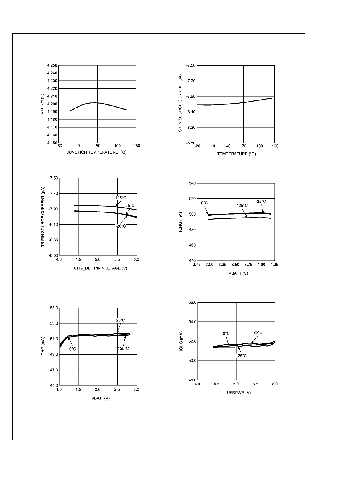
Typical Performance Characteristics — Battery Charger T
A
= 25°C unless otherwise noted
Vterm 4.2V vs. Temperature
30000196
TS Pin Current vs. Temperature
30000197
TS Pin Current vs. CHG_DET
30000198
ICHG vs. VBATT
CHG_DET = 5.0V, CC
30000199
ICHG vs. VBATT
CHG_DET = 5.0V, Prequal
I
PROG
= 500mA
30000139
ICHG vs. USBPWR
VBATT = 2.5V, Prequal
30000140
13 www.national.com
LP3913
Page 14
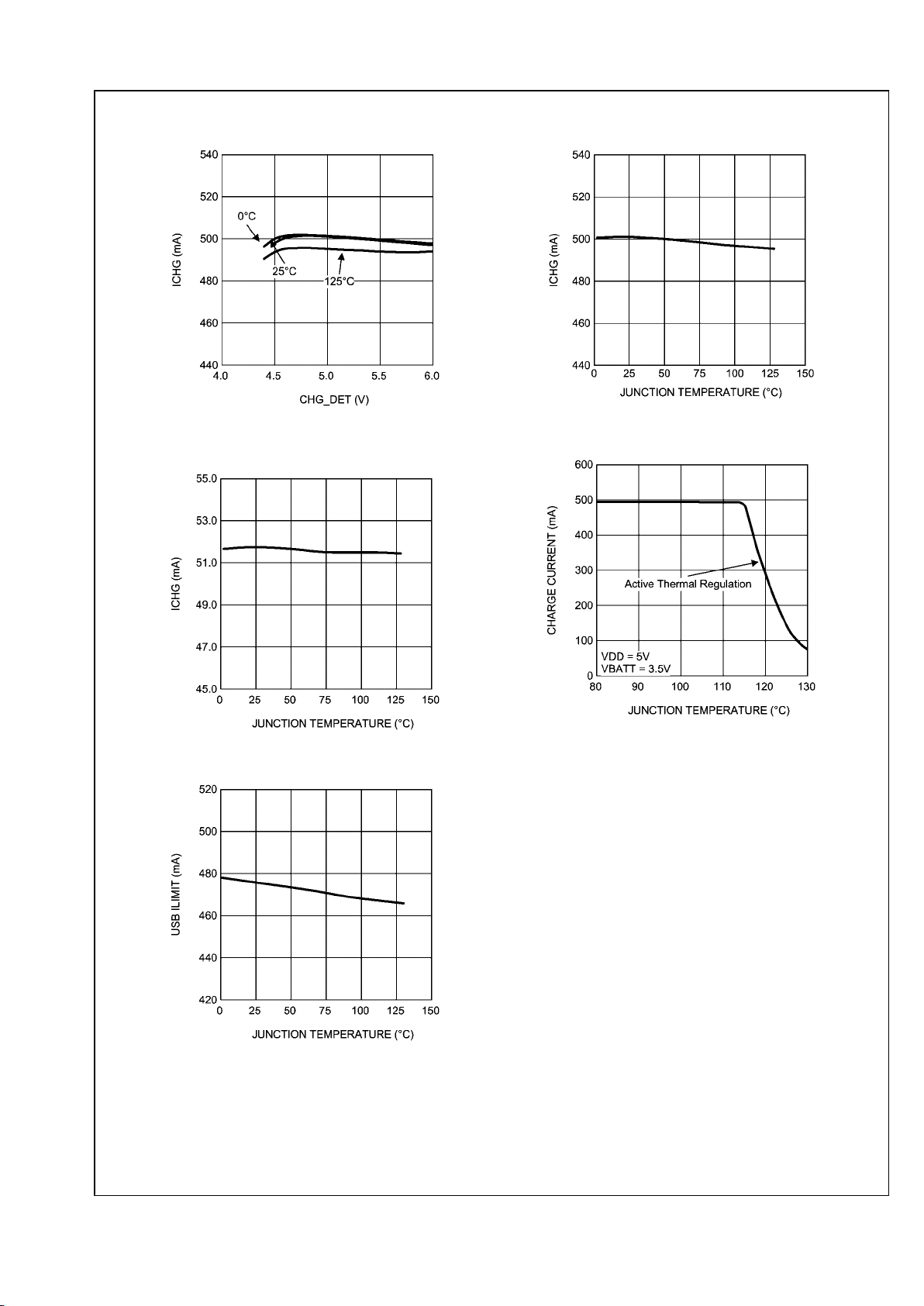
ICHG vs. CHG_DET
VBATT = 3.5V, CC
30000141
ICHG vs. Temperature
CHG_DET = 5V, VBATT = 3.75V, CC
30000142
ICHG vs. Temperature
CHG_DET = 5V, VBATT = 2.5V, Prequal
30000143
Thermal Regulation of Charge Current
30000144
USB ILIMIT vs. Temperature
30000145
www.national.com 14
LP3913
Page 15
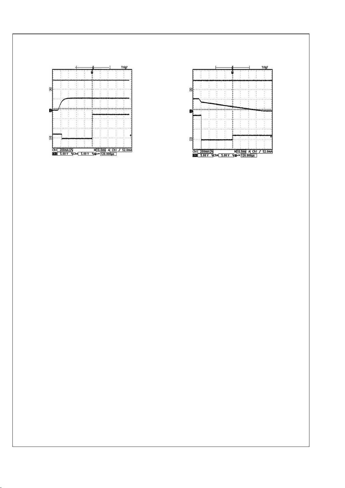
Wall Adapter Insertion with USBPWR present
CH1 = Charge Current (mA); CH3 = CHG_DET (V);
CH4 = USBPWR (V)
300001a0
Wall Adapter Removal with USBPWR present
CH1 = Charge Current (mA); CH3 = CHG_DET (V);
CH4 = USBPWR (V)
300001a1
15 www.national.com
LP3913
Page 16
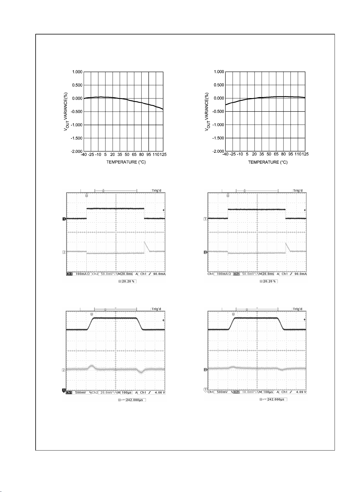
Typical Performance Characteristics — LDO T
A
= 25°C unless otherwise noted
Output Voltage Change vs Temperature (LDO1)
Vin = 4.3V, Vout = 3.3V, 100 mA load
30000146
Output Voltage Change vs Temperature (LDO2)
Vin = 4.3V, Vout = 1.8V, 100 mA load
30000147
Load Transient (LDO1)
3.6 Vin, 3.3 Vout, 0 – 100 mA load
30000148
Load Transient (LDO2)
3.6 Vin, 1.8 Vout, 0 – 100 mA load
30000149
Line Transient (LDO1)
3.6 - 4.5 Vin, 3.3 Vout, 150 mA load
30000150
Line Transient (LDO2)
3 – 4.2 Vin, 1.8 Vout, 150 mA load
30000151
www.national.com 16
LP3913
Page 17
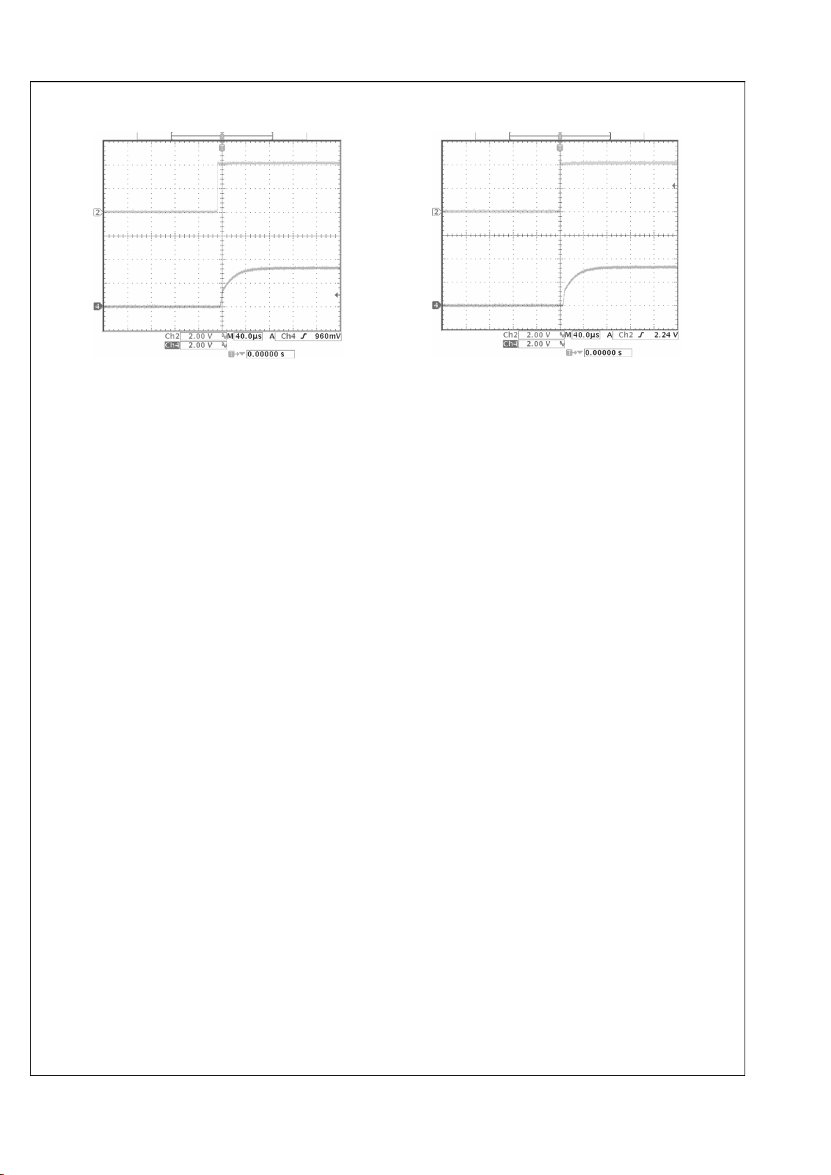
Enable Start-up time (LDO1)
0-3.6 Vin, 3.3 Vout, 1mA load
30000152
Enable Start-up time (LDO2)
0 – 3.6 Vin, 1.8 Vout, 1 mA load
30000153
17 www.national.com
LP3913
Page 18
Typical Performance Characteristics - Buck T
A
= 25°C unless otherwise noted
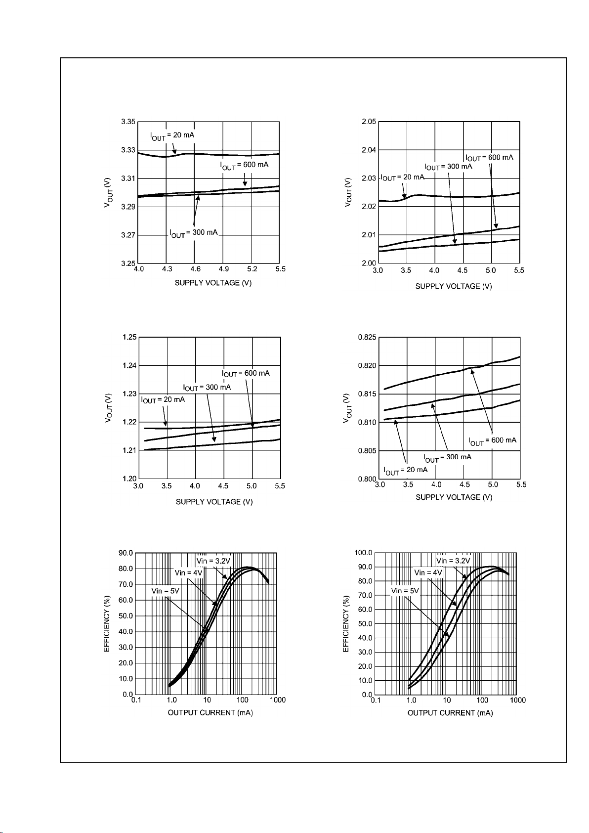
Output Voltage vs. Supply Voltage
(Vout = 3.3 V)
30000154
Output Voltage vs. Supply Voltage
(Vout = 2.0 V)
30000155
Output Voltage vs. Supply Voltage
(Vout = 1.2V)
30000156
Output Voltage vs. Supply Voltage
(Vout = 0.8V)
30000157
Buck 1 Efficiency vs Output Current
(Forced PWM Mode, Vout =1.2V, L= 2.2µH)
30000158
Buck 1 Efficiency vs Output Current
(Forced PWM Mode, Vout =2.0V, L= 2.2µH)
30000159
www.national.com 18
LP3913
Page 19

Buck 1 Efficiency vs Output Current
(PFM to PWM mode, Vout =1.2V, L= 2.2µH)
30000160
Buck 1 Efficiency vs Output Current
(PFM to PWM mode, Vout =2.0V, L= 2.2µH)
30000161
Buck 2 Efficiency vs Output Current
(Forced PWM Mode, Vout =1.8V, L= 2.2µH)
30000162
Buck 2 Efficiency vs Output Current
(Forced PWM Mode, Vout =3.3V, L= 2.2µH)
30000163
Buck 2 Efficiency vs Output Current
(PFM to PWM Mode, Vout =1.8V, L= 2.2µH)
30000164
Buck 2 Efficiency vs Output Current
(PFM to PWM Mode, Vout =3.3V, L= 2.2µH)
30000165
19 www.national.com
LP3913
Page 20

Buck 1 Load Transient Response
VIN = 4.2V, VOUT = 1.2V
ILOAD = 200-400mA (PWM Mode)
30000166
Buck 1 Load Transient Response
VIN = 4.2V, VOUT = 1.2V
ILOAD = 50-150mA (PFM to PWM)
30000167
Buck 2 Load Transient Response
VIN = 4.2V, VOUT = 3.3V
ILOAD = 200-400mA (PWM Mode)
30000168
Buck 2 Load Transient Response
VIN = 4.2V, VOUT = 3.3V
ILOAD = 50-150mA (PFM to PWM)
30000169
Line Transient Response
Vin = 3 – 3.6 V, Vout = 1.2 V, 250 mA load
30000170
Line Transient Response
Vin = 3.6 – 4.2 V, Vout = 3.3 V, 250 mA load
30000171
www.national.com 20
LP3913
Page 21

Start up into PWM Mode
Vout = 1.8 V, 30 mA load
30000172
Start up into PWM Mode
Vout = 3.3 V, 30 mA load
30000173
Start up into PFM Mode
Vout = 1.8 V, 30 mA load
30000174
Start up into PFM Mode
Vout = 3.3 V, 30 mA load
30000175
21 www.national.com
LP3913
Page 22

Typical Performance Characteristics - Buck3 T
A
= 25°C unless otherwise noted
Efficiency vs. VIN
ILOAD = 100mA
30000176
Forced PWM Efficiency vs ILOAD
VOUT = 3.3V
30000177
AutoMode Efficiency vs. ILOAD
VOUT = 3.3V
30000178
AutoMode Efficiency vs. ILOAD
VOUT = 1.8V
30000179
Buck3 Load Transient Response
VIN = 4.2V, VOUT = 3.3V,
ILOAD = 0-100mA (PFM Mode)
30000184
Buck3 Load Transient Response
VIN = 3.6V, VOUT = 3.3V
ILOAD = 150-250mA (PWM Mode)
30000185
www.national.com 22
LP3913
Page 23

Line Transient Response
VIN = 3.6 - 4.2V, VOUT = 3.3V, ILOAD = 80mA
30000186
Line Transient Response
VIN = 3.6 - 4.2V VOUT = 3.3V, ILOAD = 260mA
30000187
23 www.national.com
LP3913
Page 24

Functional Description
OPERATING MODES
The LP3913 can be in 3 different operating modes as illustrated in the following Operating Mode State Diagram:
30000103
State Machine Definitions:
V
BLA
Battery low alarm threshold
V
BATT
Battery voltage
WA
Wall Adapter
USB
Universal Serial Bus Adapter
ONOFF
On off pin event
POWERACK
Acknowledgment from the Host Processor
www.national.com 24
LP3913
Page 25

Voltage Threshold Levels
30000104
25 www.national.com
LP3913
Page 26

Power State Table
Power Off Standby Active Charger Standby
LDO1,2 Off Off On Off
BUCK1,2 Off Off On Off
BUCK3 Off Off On Off
CHARGER Off Off On if Charger / USB Present On if Charger / USB Present
A/D Converter Off Off On Off
NRST Low Low High Low
I2C interface Off Off On Off
Internal System Oscillator Off Off On On
Battery Monitor Off On On On
Current consumption <1 µA 10 µA (typ) See Electrical Characteristics See Electrical Characteristics
Power-On-Reset
The LP3913 is equipped with an internal Power-On-Reset
(“POR”) circuit that will reset the logic when VDD < V
POR
. This
guarantees that the logic is properly initialized when VDD rises
above the minimum operating voltage of the Logic and the
internal oscillator that clocks the Sequential Logic in the Control section.
Thermal Shutdown and Thermal Alarm
An internal temperature sensor monitors the junction temperature of the LP3913 and forcibly invokes standby mode in the
unusual case when the junction temperature of the silicon exceeds the normal operating level due to excessive loads on
all power regulators and the Li-ion charger and/or due to an
abnormally high ambient temperature. The thermal Shutdown
threshold is 160°C.
The thermal shutdown is preceded by a Thermal alarm that
generates an interrupt request if unmasked (see Interrupt Request generation). The temperature threshold for triggering
the alarm is 115°C.
NRST Pin
The NRST pin is an open-drain output and is active low during
Standby, Power Off and Charger Standby modes. The NRST
timing is determined by a factory programmable counter.
Control Registers
The LP3913 contains 14 user programmable registers that
configure the functionality of the individual modules inside the
IC. Registers are programmed through an I2C interface and
have default values that are invoked during an internal reset.
Some of the default values can be tailored to the specific
needs of the system designer (see Application Notes).
Throughout this product specification, the register address is
noted in hexadecimal notation immediately following the register name as illustrated below:
PON Register (00)h Power On Event Register
D7–4 D3 D2 D1 D0
Battery Monitor
The battery voltage is monitored and will invoke the Power
Off mode when the battery low threshold is breached for more
than 5 ms (Typ.). The battery low threshold DEFAULT is factory programmed. The battery low threshold range is 2.5V–
3.5V with steps of 50 mV. The Battery low threshold in the
table below refers to a decreasing battery voltage. The threshold when the battery voltage is transitioning out of the
V
BATTLOW
is 50 mV (Typ.) higher than the values listed in the
table below due to a built-in hysteresis of 50 mV (Typ.).
The battery low IRQ is triggered 200 mV above the battery
low alarm threshold that powers down the IC. This gives the
user time for a controlled shutdown.
www.national.com 26
LP3913
Page 27

BATTLOW Register (04)h Battery Low Alarm Register
D7–5 D4–0
Access Read Only 0 rw
Data reserved Battery Low threshold voltage (V) Battery low IRQ threshold Voltage (V)
5’h14–1F 2.50 2.70
5’h13 2.55 2.75
5’h12 2.60 2.80
5’h11 2.65 2.85
5’h10 2.70 2.90
5’h0F 2.75 2.95
5’h0E 2.80 3.00
5’h0D 2.85 3.05
5’h0C 2.90 3.10
5’h0B 2.95 3.15
5’h0A 3.00 3.20
5’h09 3.05 3.25
5’h08 3.10 3.30
5’h07 3.15 3.35
5’h06 3.20 3.40
5’h05 3.25 3.45
5’h04 3.30 3.50
5’h03 3.35 3.55
5’h02 3.40 3.60
5’h01 3.45 3.65
5’h00 3.50 3.70
Reset n/a 5’h0C 2.90 3.10
PowerOff Mode
In Power Off mode the main battery, the battery charger supply, and the USB supply are below their minimum on levels.
All internal circuits are disabled as the supply voltage is below
the level to activate them. The LP3913 is in Power Off mode
when the battery voltage is below the battery V
UVLO
(2.4V typ)
except when a valid external supply is detected.
Standby
When the LP3913 is in Standby Mode, the chip is waiting for
a valid power-on event to transition to Active Mode. There are
3 valid wakeup signals. First is the ONOFF pin. Second is Wall
Adapter Insertion. Third is the USB insertion. V
BATT
must be
greater than the battery V
UVLO
in order to stay in Standby
Mode, otherwise the chip transitions to Power Off Mode.
Standby Mode is skipped when advancing from Power Off
Mode when a battery is inserted that is above the battery low
alarm threshold.
If the battery is below the battery low alarm threshold, Power
Off Mode transitions to Standby Mode. However, hot insertion
of the battery with the adapter connected is NOT permitted.
In Standby Mode, the current consumption is reduced to I
Q
(10 µA TYP).
Active Mode
All LP3913 circuits are fully operational in Active mode.
Power On/Off Sequencing
Each DC/DC converter (Buck1, Buck2, Buck3, LDO1, LDO2)
and the NRST pin of the LP3913 has its own delay after which
it is enabled following a power-on event or disabled following
a power-off event. Following the deglitching of the power-on
event, the system bandgaps are enabled. Following this is a
5 ms delay that internal circuitry requires to cleanly powerup.
The programmable delays are measured from this time point.
Following the deglitching of a power-down event (up to 5 ms
if POWERACK pin is used), the power-down sequencer will
start. Each delay ranges from 0 ms to 63 ms in steps of
1 ms and is factory programmed to the desired values submitted by the system designer. As illustrated below, the power-on/off sequencing is designed around a 6-bit up/down
timer that is clocked at 1 kHz. A power-on or power-off event
will trigger the timer, which counts up from 0 during a poweron sequence and counts down from 5'b11111 during a powerdown cycle. The timer output is connected to 5 comparators
with factory programmed timeout values that correspond to
the on and off delays for each DC/DC converter and the NRST
pin. Once the timer has incremented beyond the comparator
timeout value during a power-on cycle, the output of the comparator enables the corresponding DC/DC converter or raises
the NRST pin to a logic high level. Subsequently, once the
timer has decremented below the comparator timeout value
during a power-down cycle, the output of the comparator will
disable the corresponding DC/DC converter or will activate
the NRST pin to a logic low level.
27 www.national.com
LP3913
Page 28

Power up sequence:
30000105
Power On Timing
Each timeout T1 thru to T5 are factory programmed from 0 ms to 63 ms. The following defaults are shown below.
Symbol Description Time Units
T1 Programmable Delay for LDO1 and LDO2 5 ms
T2 Programmable Delay to Buck1 15 ms
T3 Programmable Delay for Buck2 20 ms
T4 Programmable Delay for Buck3 25 ms
T5 Programmable Delay for NRST 60 ms
Power Off Timing
The timing delays during a power off sequence are equal to 63 ms minus the timing delay during the power on sequence.
Symbol Description Time Units
T1 Programmable delay for LDO1 and LDO2 58 ms
T2 Programmable delay to Buck1 48 ms
T3 Programmable delay for Buck2 43 ms
T4 Programmable delay for Buck3 38 ms
T5 Programmable delay for NRST 3 ms
Transitioning from Standby to Active Mode (Power Up)
Battery Power Present Only
When only battery power is present and the battery voltage
V
BATT
> V
BATTLOW
, the LP3913 is waiting for one of three valid
wakeup signals. The first is the ONOFF pin. The second and
third wakeups are the Wall Adapter and USBPWR. The
ONOFF pin is factory programmable wakeup source. It can
be a rising edge, a falling edge, a level high, or a level low
event. Regardless of the mode, the signal requires a 32 ms
deglitch time. A deglitched version of the ONOFF pin is output
on the open-drain output pin ONSTAT. ONOFF is usually
connected to a push button. Asserting the ONOFF pin starts
the power on sequencer. This enables the DC/DC converters
including the Buck1 DC/DC converter that supplies power to
the system processor. The system processor then needs to
set bit D4 (PACK bit) in the Power On Event Register through
the I2C interface or apply a logic high to the POWERACK pin
to keep the LP3913 in the Active mode. These serve as a
Power Acknowledgement, confirming the power on request
initiated by the ONOFF pin. If neither the PACK bit (D4) in the
PON register or the POWERACK pin is set within 128 ms
(max) of the start of the power-up sequencer, then the LP3913
will automatically turn off, as the system failed to acknowledge
the power on request. Connecting the battery will be considered a Power on event. However hot insertion of the battery
with the adapter connected is NOT permitted.
www.national.com 28
LP3913
Page 29

PON Register (00)h Power On Event Register
D7–5 D4 D3 D2 D1 D0
Access Read Only 0 rw Read Only
Data Reserved PACK Battery Insert PON by ONOFF PON by CHG_IN PON by USB
Power
0: Disable Power,
go in standby, and
wait for power on
event.
0: default 0: default 0: default 0: default
1: Acknowledge
Power On request
1: Battery Insert
caused by Battery
Insertion
1: ONOFF caused
Power On event
1: Power On caused
by CHG_IN power
detection
1: Power On caused
by USB power
detection
Reset n/a 0 0 0 0 0
External Power and Battery Detection
When a Wall Adapter is detected, regardless of the battery
voltage, the LP3913 moves to the Active Mode and the Power-up sequencer is started. Similar to the ONOFF pin, there
is a 32 ms deglitch time to ensure a clean wall adapter detection and the system processor needs to set the PACK bit
(D4) in the PON register or the POWERACK pin within 128
ms (max) of the start of the power-up sequencer.
When USB PWR is detected and the battery is above the low
battery alarm threshold, the LP3913 moves to the Active
Mode and the Power-up sequencer is started. Similar to the
ONOFF pin, there is a 32 ms deglitch time to ensure a clean
USB detection and the system processor needs to set the
PACK bit (D4) in the PON register or the POWERACK pin
within 128 ms (max) of the start of the power-up sequencer.
If the battery is below the low battery alarm threshold, the
system will remain powered down until the USBPWR charges
the battery up to the battery low alarm threshold, at which
point the power-up sequencer is started.
The four LSB bits of the PON register indicate which PON
source was responsible for moving the LP3913 out of standby
and into active mode:
Battery insert
ONOFF push button
CHG_IN detect (connection of power adapter)
USB power (plug-in of powered USB cable)
These bits are cleared upon powering off.
29 www.national.com
LP3913
Page 30

Power Up Sequence
30000106
TRANSITIONING FROM ACTIVE MODE TO STANDBY
MODE
External Event Triggers the Transition from Active to
Standby Mode
When the device is active, a subsequent re-assertion of the
push button will turn off the LP3913 indirectly by first flagging
the system processor though the ONSTAT pin. Upon detecting the ONSTAT transition, the system processor must clear
bit D4 (PACK) in the Power On Event Register and apply a
logic low to the POWERACK pin to power down the LP3913,
which then transitions to Standby Mode. Clearing the PACK
register bit and POWERACK pin while external supply
sources are present (either USB or CHG_IN) will not power
down the LP3913, to keep the charger active. The system can
as always disable all necessary DC/DC converters, except
BUCK1, through the register control.
When external power is disconnected, LP3913 will remain in
its Active state unless the battery voltage is below V
BLA
(Battery Low Alarm) or unless the PACK (either bit D4 in the PON
register and the POWERACK pin) is cleared by the system
processor.
www.national.com 30
LP3913
Page 31

Power Down Caused by External Event
30000107
Transition from Active to Standby Mode Due to Expiring
POWERACK Deadline
With no external charger present when the system processor
fails to acknowledge the power-on in time by setting either the
PACK bit (D4) in the PON register or the POWERACK pin
before the 128 ms deadline following the start of the powerup sequencer, then the NRST is immediately de-asserted and
after 2 ms all power sources will be disabled before transitioning to Standby Mode. This 2 ms delay allows the microprocessor to receive a clean reset before the power is de-
asserted. A new power-on event is then required to transition
back to Active mode.
With either external charger present when the system processor fails to acknowledge the power-on in time by setting
either the PACK bit (D4) in the PON register or the POWERACK pin before the 128 ms deadline following the start of the
power-up sequencer, then the NRST is immediately de-asserted and after 2 ms all power sources will be disabled before
transitioning to Charger Standby Mode.
31 www.national.com
LP3913
Page 32

Power Down Caused by Expiring PowerACK Deadline
30000108
Transition from Charger Standby Mode to Either Active
or Standby Mode
While in Charger Standby mode, the battery is charged using
the default values of I
PROG
, EOC, V
TERM
, Batt Temp Range
and USB I
SEL
. In Charger Standby mode, all the regulators
and the I2C are disabled. A new power-on event is required
to transition back to Active Mode. Removing the charger during Charger Standby Mode causes a transition back to Standby Mode.
www.national.com 32
LP3913
Page 33

I2C COMPATIBLE SERIAL INTERFACE
I2C Signals
The LP3913 features an I2C compatible serial interface, using
two dedicated pins: I2C_SCL and I2C_SDA for I2C clock and
data respectively. Both signals need a pull-up resistor according to the I2C specification. The LP3913 interface is an
I2C slave that is clocked by the incoming SCL clock.
Signal timing specifications are according to the I2C bus specification. The maximum bit rate is 400 kbit/s. See I2C specification from Philips for further details.
I2C Data Validity
The data on I2C_SDA line must be stable during the HIGH
period of the clock signal (I2C_SCL), e.g., the state of the data
line can only be changed when CLK is LOW.
I2C Signals: Data Validity
30000109
I2C START and STOP Conditions
START and STOP bits classify the beginning and the end of
the I2C session. The START condition is defined the as the
I2C_SDA signal transitioning from HIGH to LOW while SCL
line is HIGH. The STOP condition is defined as the SDA transitioning from LOW to HIGH while I2C_SCL is HIGH. The I2C
master always generates START and STOP bits. The I2C bus
is considered to be busy after a START condition and free
after a STOP condition. During data transmission, I2C master
can generate repeated START conditions. First START and
repeated START conditions are equivalent, function-wise.
START and STOP Conditions
30000110
Transferring Data
Every byte put on the I2C_SDA line must be eight bits long,
with the most significant bit (MSB) being transferred first.
Each byte of data has to be followed by an acknowledge bit.
The acknowledged related clock pulse is generated by the
master. The transmitter releases the I2C_SDA line (HIGH)
during the acknowledge clock pulse. The receiver must pull
down the I2C_SDA line during the 9th clock pulse, signifying
acknowledgement. A receiver which has been addressed
must generate an acknowledgement (“ACK”) after each byte
has been received.
Register Write Cycle
After the START condition, the I2C master sends a chip address. This address is seven bits long followed by an eighth
bit which is a data direction bit (R/W). For the eighth bit, a “0”
indicates a WRITE and a “1” indicates a READ. The second
byte selects the register to which the data will be written. The
third byte contains data that will be written to the selected
register.
LP3913 has a chip address of 60’h, which is set by a metal
mask option.
I2C Chip Address
30000111
33 www.national.com
LP3913
Page 34

I2C Write Cycle
30000112
w = write (I2C_SDA = “0”)
r = read (I2C_SDA = “1”)
ack = acknowledge (I2C_SDA pulled down by either master or slave)
rs = repeated start
id = LP3913 chip address : 60’h
Register Read Cycle
When a READ function is to be accomplished, a WRITE function must precede the READ function, as shown in the Read
Cycle waveform.
I2C Read Cycle
30000113
Multi-byte I2C Command sequence
The LP3913’s I2C serial interface shall support Random register Multi-byte command sequencing: During a multi-byte
write the Master sends the Start command followed by the
Device address, which is sent only once, followed by the 8bit register address, then 8 bits of data, The I2C slave must
then accept the next random register address followed by 8
bits of data and continue this process until the master sends
a valid stop condition.
A Typical Multi-byte random register transfer is outlined below:
Device Address, Register A Address, Ack, Register A Data,
Ack Register M Address, Ack, Register M Data, Ack Register X Address, Ack, Register X Data, Ack Register Z Address, Ack, Register Z Data, Ack, Stop
Note:
the PMIC is not required to see the I2C device address for each
transaction. A, M, X, and Z are random numbers
30000114
www.national.com 34
LP3913
Page 35

LI-ION LINEAR CHARGER
Charger Architecture
The LP3913 can safely charge and maintain a single cell LiIon/Polymer battery operating off a regulated 6V Car adapter,
AC wall adapter, or USB power (VBUS). Input power source
selection of USB/adapter is seamless. If present, the charger
will use the adapter power regardless of the presence of USB
power. The connection of either power source is detected by
LP3913.
30000115
The charger module is a linear charger with constant current
pre-qualification, constant current (“CC”) full-rate charging
and constant voltage (“CV”) charging. CC and CV regulation
is performed using an internal Power FET Q2 with reverse
current blocking. The termination voltage is controlled to within ±0.35% at room temperature.
The power FET Q1 acts as a switch with programmable current limit for USB operation.
35 www.national.com
LP3913
Page 36

30000116
Charge Status Indication
Two LEDs connected to the LP3913 are used to indicate the
status of the charging. The CHG pin is connected to a red LED
that is enabled when an external power source is connected
and the battery is charging. The second STAT pin is connected to a green LED. When the battery charging transitions from
CC to CV mode, then the green LED is blinking with a 50%
duty cycle and a period of 1 second. When the battery is fully
charged, then the green LED is always on.
Both LEDs are off when there is no external power connected.
Truth table for the LED status indicators.
Condition RED LED GREEN LED
No Charger or USB OFF OFF
Charger off ON OFF
Condition RED LED GREEN LED
Pre-Qualification ON OFF
Constant Current CC ON OFF
Constant Voltage CV ON 50% duty
cycle
EOC / Top-OFF charging ON ON
Charge cycle complete ON ON
ERROR (Battery Temp,
Thermal shutdown)
50% duty
cycle
OFF
Safety Timer Expired 50% duty
cycle
OFF
50% duty cycle indicates the LED is pulsed on/off for equal
times at a frequency of 1 Hz.
The RED pin and GREEN pin are connected to a regulated
driver to ensure that the brightness is independent from the
external power. The LEDs need to be connected between the
CHG / STAT pins and GND.
Thermal Charger Power FET Regulation
The internal power FET Q2 in the linear charger module is
thermally regulated to the junction temperature of 115°C to
guarantee optimal charging of the battery. The charge current
is limited by the charge current selected in the Charger Control Register but is also thermally limited to prevent the junction from overheating during high charge currents at high
ambient temperatures as the package power dissipation is
limited.
Thermal regulation guarantees maximum charge current and
superior charge rate without exceeding the power dissipation
limits of LP3913.
CHCTL Register (01)h Charger Control Register
D7–6 D5–2 D1 D0
Access rw
Data Termination voltage ICC: Full Rate Charge
current
Charger enable End of Charge Select
00: 4.1V (Li Ion)
01: 4.2V (Li Polymer )
10: 4.38V (Li Polymer)
11: reserved
0000: 100 mA
0001: 200 mA
0010: 300 mA
0011: 400 mA
0100: 500 mA
0101: 600 mA
0110: 700 mA
0111: 800 mA
1000: 900 mA
1001: 1000 mA
0: disabled
1: enabled
0: 5%
1: 10%
Reset 01 0000 1 1
BATTERY CHARGER OPERATING MODES
Pre-Qualification Mode
Lithium batteries cannot be subjected to a high current when
the battery voltage is under a certain threshold, otherwise the
longevity of the battery would be compromised. Below this
threshold of V
FULLRATE
, which typically measures 2.85V, the
charger circuit supplies a pre-qualification charge current. If
the wall adapter is charging the battery, the charger circuit
supplies a constant current of 10% of the programmed charge
current. If the USB is charging the battery, the charger circuit
supplies a constant 50 ma charge current. When the battery
voltage reaches V
FULL_RATE
, the charger transitions from prequalification to full-rate charging. In Pre-qualification mode,
the STAT2, STAT1, and STAT0 bits in the charger supervisory register are respectively low, low, high.
www.national.com 36
LP3913
Page 37

Full-Rate Charging Mode
The full-rate charge cycle is initiated following the successful
completion of the pre-qualification mode. During Full-Rate
charging, the battery voltage steadily increases while charged
with a constant current (CC). The three charger status bits
STAT2, STAT1 and STAT0 are respectively low, high, and
low. The full-rate charge current is selected using the Charge
Control Register, which defaults to 100 mA.
It is recommended to charge Li-Ion batteries at a rate of 1C,
where “C” is the capacity of the battery. As an example, it is
recommended to charge a battery with a capacity of
800 mAh at 800 mA, or 1C. Charging at a higher rate may
compromise the quality and lifetime of the battery.
Constant-Voltage (CV) Charging Mode
The battery voltage increases rapidly as a result of full-rate
charging and once it reaches the programmable termination
voltage of either 4.1V, 4.2V or 4.38V, the charger will move
to constant-voltage charge mode. During this mode, the
charge current gradually decreases while the battery remains
at the termination voltage. The termination voltage can be
selected to be either 4.1V, 4.2V or 4.38V by programming bits
D6 and D7 in the Charger Control register to accommodate
different battery chemistries. In CV charging mode, the
Charge Control Status bits STAT2, STAT1 and STAT0 are
respectively logic 0, logic 1 and logic 1.
TOP-OFF Charging Mode
When the charge current reduces to the EOC threshold (programmable to 5% or 10% of programmed full rate charge
current), constant voltage charging will continue for an additional 21 minute TOP-OFF time period. In TOP-OFF charging
mode, the Charge Control Status bits STAT2, STAT1 and
STAT0 are respectively logic 1, logic 1 and logic 1. At the end
of the TOP-OFF period, the charger transitions to Charge Cycle Complete.
Charge Cycle Complete
During Charge Cycle Complete, the charger is automatically
disabled, regardless of the state of the Charge Enable Bit. In
Charge Cycle Complete, the STAT2, STAT1 and STAT0 bits
are respectively logic 1, logic 0 and logic 1. When the Battery
Voltage drops below the V
RESTART
threshold, charging will re-
sume in Full-Rate Charging Mode.
30000117
Battery Temperature Monitoring (TS pin)
The LP3913 is equipped with a battery thermistor terminal to
continuously monitor the battery temperature by measuring
the voltage between the TS pin and GND. With the TS pin
connected to the battery thermistor, charging is allowed only
if the battery temperature is within the acceptable temperature range set by a pair of internal comparators inside the
LP3910. The temperature window is 0°C–45°C or 0°C–50°C,
depending on the setting of D2 of the Charger Supervisory
(CHSPV) register. There is 3ºC of temperature hysteresis associated with each temperature threshold. The default temperature range is 0°C–50°C and can be changed to 0°C–45°
C by setting bit D3 in the CHSPV register. If the battery temperature is out of range, STAT2, STAT1 and STAT0 bits in
the CHSPV Register are set to logic1, logic0, logic0, and
charging is suspended.
The TS pin is only active during charging and draws no current
from the battery when no external power source is present.
If the TS pin is not used in the application, it should be connected to GND through a 100 kΩ pulldown resistor.
When the TS pin is left floating (battery removal), then the
charger will be disabled as the TS voltage exceeds the lower
temperature limit.
30000118
Disabling Charger
Charging can be safely interrupted by clearing the Charge
enable bit D1 in the Charge Control Register and can subsequently resume upon setting this bit. When the charger is
disabled, STAT2, STAT1, and STAT0 bits in the CHSPV register are set to logic 0.
Safety Timer
In order to prevent endless charging, which could degrade the
battery quality and life time, the LP3913 contains a safety
timer that limits charging regardless whether the battery has
reached its full capacity or not. In prequalification the safety
timer is 1 hour. In full rate or constant voltage charging the
37 www.national.com
LP3913
Page 38

safety timer is a maximum of 10 hours minus the time in prequalification.
When the timer times out of uninterrupted charging, an IRQ
is generated to alert system processor. The status of the timer
can also be polled by reading the IRQ register if the system
doesn’t support hardware interrupts.
The Safety timer resets and starts counting from zero upon
the following events:
1.
Power ON (through connecting valid power to either
USBPWR or CHGN_IN pins).
2.
Interchanging USBPWR and CHG_IN sources
3.
The voltage of a charged battery drops below the restart
value and the charger is enabled
4.
Disabling and re-enabling of the charger by toggling bit
D1 of the Charge Control Register
5.
Emerging from Thermal Shutdown
6.
Emerging from a battery temperature out-of-range and
the charger is enabled
7.
Emerging from USB suspend mode when charging with
USB power
Charging Maintenance
When a fully charged battery is being loaded by the system
while the external power is present and while bit D1 in the
charge control register is set to a 1 (Charge enable) then the
charging will restart when the battery voltage drops below the
charging restart threshold. The value of the threshold depends on the termination voltage according to the following
table:
Vterm Charging restart voltage
4.1V 3.9V
4.2V 4.0V
4.38V 4.2V
CHSPV Register (02)h Charger Supervisor Register
D7–6 D5 D4 D3 D2–0
Access Read only r/w r/w r/w
Data Reserved LED Current LED ENABLE
0: Disabled
1:Enabled
Battery
temperature
range
Charger status
0: 5 mA 0: 0°C–50°C Stat2 Stat1 Stat0
1: 10 mA 1: 0°C–45°C 0 0 0 Charger is off
0 0 1 Prequalification
0 1 0 Constant current
charging
0 1 1 Constant voltage
charging
1 0 0 Error
1 0 1 Charge cycle
complete
1 1 0 Safety Timer Expired
1 1 1 EOC / Top-off
Reset n/a 1 1 0 2’b000
POWER ROUTING
The LP3913 power can originate from three different sources:
Adapter power, USB power or battery power. The objective
of the power routing is to be able to:
•
Operate the portable system from external power
regardless of the battery voltage.
•
Operate the portable system from USBPWR when the
battery exceeds the Full Rate Qualification Threshold
voltage (Vfullrate).
•
Concurrently charging and operating the system when
external power is present
•
Seamless selection of Adapter or USB power as the
primary external power source
Power Routing supports 4 modes:
1.
A regulated external adapter power is present and
concurrently supplies the system power and the battery
charger.
2.
USB power is present and supplies the system and the
battery.
3.
USB power is present but the system demand exceeds
the USB current limit, so that the battery provides the
additional power to operate the system.
4.
The battery is the sole supply source to the system when
no external power source is present
The current flows in the different modes are realized through
internal FETS and an external Schottky as illustrated as follows:
www.national.com 38
LP3913
Page 39

30000119
The current provided by the external adapter power or USB
power, when inserted, first supplies the system load; the remainder is used for charging.
The different paths are configured through two internal power
FETs, Q1 and Q2, and an external Schottky diode. Q1 is a
Power FET that is only active during USB charging. Q2 functions either as a linear Power FET during charging or as a low
R
DSON
switch when no external power is present and the bat-
tery discharges to supply power to the system.
Power Route Q1 Q2
Regulated adapter supply &
battery charging
OFF Regulated
USB supply & battery charging ON Regulated
No external supply &
battery discharging
OFF ON
The Power Routing function will allocate power to the system
through the VDD pin and to the battery. V
DD1
, V
DD2
, V
DD3
,
V
IN1
, V
IN2
, V
IN3
, and V
IN4
must be connected together exter-
nally. V
BATT1
, V
BATT2
, and V
BATT3
must be connected together
externally.
USB SUSPEND MODE
The LP3913 USB current consumption can be disabled during suspend mode through a dedicated pin (USBSUSP).
Applying a logic 1 to this pin will disable the USB current path
and current is reduced to input leakage current less than
30 µA on the USBPWR pin.
SETTING THE USB CURRENT LIMIT
The USB current that is available from the USB on the VBUS
wire is limited by default to 100 mA. More current (up to
800 mA) can be negotiated through a session request protocol between host and peripheral. The USB current limit needs
to be signaled to the LP3913 by means of the USB
ISEL
pin or
the I
LIMIT
Register as indicated below.
If the USB current limit is 100 mA then the USB controller of
the peripheral system needs to set the USB
ISEL
logic 0 or by
setting the I
LIMIT
register bits [D1, D0] to 2’b00.
If the USB current limit is 500 mA, then the USB controller
needs to apply logic 1 to the USB
ISEL
pin or change the I
LIM-
IT
register accordingly. Under this condition, the LP3913 will
allow charging with a charge current that is determined by the
Charge Control Register, not exceeding 500 mA.
The LP3913 will prevent (through internal circuitry) the charge
current from exceeding the USB current limit, even if the current setting in the Charge Control Register exceeds 500 mA.
The controller can also select a USB current limit of 800 mA
through I2C that exceeds current USB spec values.
I
LIMIT
REGISTER (03)h CURRENT LIMIT REGISTER
D7–2 D1–0
Access Read only 0
Data Reserved USB Current Limit
00: controlled by USB
ISEL
pin
[low = 100 mA, high = 500 mA]
01: 100 mA
10: 500 mA
11: 800 mA
Reset n/a 2’b00
39 www.national.com
LP3913
Page 40

ANALOG TO DIGITAL CONVERTER
LP3913 is equipped with an 8-bit dual-slope integrating analog to digital converter. Dual-slope converters provide effective filtering of >500 kHz and <125 kHz noise components on
the input voltage, and does not require a sample and hold
stage. The A/D converter core digitizes the input voltage
ranging from V
REF
to 2V
REF
, where V
REF
is the voltage mea-
sured on the V
REFH
pin. After an initial 2 ms warm-up for the
first activation of the ADC enable bit, the dual-slope converter
integrates the input signal during the first phase for approximately 2 ms, followed by a second phase that integrates
V
REF
for 0 ms to 2 ms depending on the level of the input
signal. As a result the total conversion time varies from 2 ms
to 4 ms.
Simplified ADC Block Diagram
30000120
The A/D converter multiplexes 4 different sources:
1.
The battery voltage
2.
The battery charge current
3.
External source ADC1
4.
External source ADC2
The voltage ranges for the first two sources are scaled to
match the input voltage interval of the A/D converter: [V
REFH
,
2V
REFH
]. This is accomplished by using two internal scalars.
Battery Voltage Measurement
The battery voltage scalar transforms the battery voltage
ranging from 2.6V–3.5V to the reference voltage interval:
[V
REFH
, 2*V
REFH
]. A wider voltage range (2.6V–4.4V) can be
selected through I2C by setting the voltage range bit D7 in
register 0xA to 0’b1.
Battery Charge Current Measurement
The battery charge current is indirectly measured by measuring the voltage across the I
SENSE
resistor. A fixed portion of
the battery charge current is mirrored over the I
SENSE
resistor
and hence:
V
ISENSE
= K * I
CHARGE
where K is a ratio between the R
SENSE
current and the charge
current.
The battery charge current scalar transforms the voltage
across the external I
SENSE
resistor to the [V
REFH
, 2*V
REFH
] in-
put voltage interval of the A/D converter.
30000121
External General Purpose Sources
Two additional A/D converter sources are available on the
ADC1 and ADC2 pins of the LP3913. These two external A/
D converter sources are not internally scaled and have an
input voltage range of [V
REFH
, 2*V
REFH
]. The system designer
can use these two sources for general purpose applications
such as resistive keyboard matrix scanning, temperature
measurements, battery load current, battery ID resistor measurement, etc.
www.national.com 40
LP3913
Page 41

ADC Analog Front End Block Diagram
30000122
The source selection and the access to the conversion results
are established through the I2C linked control registers: ADCC and ADCD as described below:
ADCC Register (0a)h A/D Converter Control Register
D7 D6 D5 D4 D3 D2 D1–0
Access r/w r/w Read Only r/w r/w
Data V
RANGE
I
RANGE
ADC Overflow Data Ready Start
Conversion
ADC Enable ADC source
selection
0: 2.6V–3.5V 0: 0 mA–605 mA 0: no overflow 0: no data 0: default 0: Disabled 00: battery voltage
1: 2.6V–4.4V 1: 0 mA–1100 mA 1: overflow 1: data ready 1: start
conversion
1: Enabled 01: battery charge
current
10: ADC1
11: ADC2
Reset 0 0 0 0 0 0 0
ADCD Register (0b)h A/D Converter Output Data Register
Charge current 0A to 1.1A mirrored to 0 µA to 250 µA, ADC measures voltage drop across R
SENSE
4.64 kΩ.
D7–0
Access Read Only 0
Data Battery voltage: 8’h00 = 2.6V 8’hFF = 3.5V 1 LSB = 0.9 / 256 = (3.5 mV) range 0
8’h00= 2.6V 8’hFF = 4.4V 1 LSB = 1.8 / 256 = (7.0 mV) range 1
Battery charge current 8’h00 = 0 8’hFF = 0.6463V = 605 mA range 0
8’h00 = 0 8’hFF = 1.175V = 1100 mA range 1
ADC1: 8’h00 = V
REFH
= 1.225V 8’hFF = 2*V
REFH
= 2.45 V (1 LSB = V
REFH
/256)
ADC2: 8’h00 = V
REFH
= 1.225V 8’hFF = 2*V
REFH
= 2.45 V (1 LSB = V
REFH
/256)
Reset 8’h00
The ADC is by default disabled to minimize current consumption and needs to be enabled by setting D2 in the ADCC
register. Writing a logic 1 to bit D3 in the ADC will initiate a
conversion. It is advised to select the correct ADC source before a conversion is started. The A/D converter will set bit D4
in the ADCC register upon the completion of a conversion,
which is typically 4 ms after the start of the conversion. At the
same time an interrupt request will be generated. (See Interrupt Request Register).
To save power, disable the ADC by setting bit 2 of D2 to 0.
To make repetitive starts, set bit D3 to 0 then to 1 for register
0Ah to initiate start of conversion. The interrupt driven protocol between LP3913 and the system processor is the most
efficient way to acquire data from successive measurements:
41 www.national.com
LP3913
Page 42

30000123
Interrupt Request Output
The LP3913 has the ability to interrupt the system processor
through the open drain IRQB pin, which transitions to an active logic low level upon the following 8 events:
•
USB Power detected
•
USB disconnected
•
CHG_IN Power detected
•
CHG_IN Disconnected
•
Battery low alarm
•
Thermal Alarm
•
ADC conversion completed
•
Charger safety timer time-out
The events form the interrupt sources that correspond to a
certain bit location in the Interrupt Request (IRQ) Register. All
interrupt sources can be masked by the Interrupt Mask Register (IMR). Masking the interrupt prevents the interrupt event
from asserting the IRQB pin, yet the event will still be captured
in the IRQ register, which allows the processor to poll the interrupt sources.
After an active low IRQB has been detected by the system
processor, the latter services the interrupt and will access the
IRQ register to determine which source was responsible for
the interrupt request. Reading the IRQ register will automatically clear the register to enable the capture of the next
interrupt events.
As new interrupts can occur while the I2C read cycle is clearing the IRQ register, a buffer register called Interrupt Pending
Register (IPR), not accessible through the I2C compatible interface holds the next interrupts. De-asserting the IRQB output is immediately followed by a new transition of IRQB to
logic low when an interrupt is pending.
The Interrupts are not hardware prioritized. It is up to the
firmware to determine the priority in case more than one Interrupt Request is set.
www.national.com 42
LP3913
Page 43

30000124
INTERRUPTS AND STANDBY MODE
Interrupts are captured in standby mode and can be serviced
when the system processor is enabled when the LP3913 is in
an active state.
INTERRUPT SOURCES
CHG_IN Power Detected and CHG_IN Disconnect (INT0
and INT1) An interrupt (INT0) is generated when CHG_IN
power is connected to the LP3913. Another interrupt (INT1)
will be generated upon CHG_IN power removal.
USB Power Detected and USB Disconnect (INT2 and
INT3) An interrupt (INT2) is generated when USB power is
connected to the LP3913. Another interrupt (INT3) will be
generated upon disconnecting the USB power.
Battery Low (INT4) When the battery voltage drops below
the battery low threshold IRQ, an interrupt will be generated.
This allows the processor to perform some housekeeping
tasks prior to going to standby mode.
Thermal Alarm (INT5)If the Junction Temperature of the
LP3913 exceeds 115°C, then an interrupt will be generated
ADC Conversion Done (INT6)The ADC generates an interrupt request upon the completion of a data conversion.
Charger Timer Interrupt (INT7) A charger timeout will occur
10 hours after it started (see Li-Ion Charger section) and will
subsequently request an interrupt.
IMR REGISTER (0C)H INTERRUPT MASK REGISTER
D7–0
Access r/w
Data 1: Enable INTn (n=0…7) to pull IRQB low
0: Mask Interrupt source INTn
Reset 8’h00
IRQ REGISTER (0d)h INTERRUPT REQUEST REGISTER
D7–0
Access Read only
Data 1: Interrupt IRQn (n=0…7) requested
0: No interrupt requested
Reset 8’h00
DC/DC Converters
OVERVIEW
The LP3913 provides the DC/DC converters that supply the
various power needs of the application by means of one
Buck3 (HDD driver), two Linear Low Drop Regulators (LDO1,
LDO2) and two Buck converters (BUCK1, BUCK2).
The table hereunder lists the output characteristics of the various regulators.
43 www.national.com
LP3913
Page 44

SUPPLY SPECIFICATION
Supply Load
V
OUT
(Volts)
I
MAX
Maximum Output
Current (mA)
Default (V) Range (V) Resolution (mV)
LDO1 various 2.0 1.2 to 3.3 100 150
LDO2 analog 3.3 1.3 to 3.3 100 150
BUCK1 CPU, DSP 1.2 0.8 to 2.0 50 600
BUCK2 IO, Logic,
Memories
3.3 1.8 to 3.3 100 600
BUCK3 Flash 3.3 1.8 to 3.3 50 1000
LINEAR LOW DROP-OUT REGULATORS (LDOS)
LDO1 is a regulator that can respond to fast transients and is
slated for digital loads and high bandwidth analog loads.
LDO2 is a linear regulator with a similar architecture but has
a slower transient response time with a lower noise perfor-
mance to supply analog loads. The output voltages of both
LDOs are register programmable through the I2C interface.
The default output voltages are factory programmed during
Final Test.
30000125
NO-LOAD STABILITY
The LDOs will remain stable and in regulation with no external
load. This is an important consideration in some circuits, for
example CMOS RAM keep-alive applications.
www.national.com 44
LP3913
Page 45

LDO1 CONTROL REGISTER
LDO1 can be configured through its own I2C control register.
The output voltage is programmable in steps of 100 mV from
1.2V to 3.3V. LDO1 gets enabled during the power-on sequence. Disable/enable control is provided through bit D5 in
the LDO1 control register after selecting the appropriate D4–
0 settings, which determine the output voltage.
The output voltage can be altered while LDO1 is enabled.
When LDO1 is disabled it shunts the output to AGND with a
R
SHUNT
= 200Ω (Max.).
LDO1 CONTROL REGISTER (08)h
D7–6 D5 D4–0
Access Read Only0R/W
Data Reserved Operation
0: disable
1: enable
LDO1 Output Voltage
(V)
5’h00 1.2
5’h01 1.3
5’h02 1.4
5’h03 1.5
5’h04 1.6
5’h05 1.7
5’h06 1.8
5’h07 1.9
5’h08 2.0
5’h09 2.1
5’h0A 2.2
5’h0B 2.3
5’h0C 2.4
5’h0D 2.5
5’h0E 2.6
5’h0F 2.7
5’h10 2.8
5’h11 2.9
5’h12 3.0
5’h13 3.1
5’h14 3.2
5’h15 –
5’h1F
3.3
Reset n/a 1 5’h08
45 www.national.com
LP3913
Page 46

LDO2 CONTROL REGISTER
LDO2 can be configured through its own I2C control register.
The output voltage is programmable in steps of 100mV from
1.3V to 3.3V. LDO2 is by default disabled and can be enabled
by setting bit D5 in the control register after selecting the appropriate D4–0 settings, which determine the output voltage.
LDO2 can also be enabled through the external LDO2EN pin,
which is the default enable control. With a logic 0 programmed
to bit D5 in the corresponding control register, enable/disable
control is passed onto the LDO2EN pin; a logic 1 applied to
this pin enables LDO2 while a logic 0 disables the LDO2.
Setting D5 to 1 in the LDO2 control register enables LDO2,
regardless of the state of the LDO2EN pin. If the system designer permanently connects the LDO2EN pin to GND, then
D5 is simply a enable/disable control bit. If the system design
permanently connects the enable pin to VDD, then the LDO is
enabled during the power-on sequence and will always be on,
regardless of the state of bit D5 in the LDO2 control register.
In that particular case, the LDO2 is sequenced with the same
timing as LDO1 (see Power On sequencing).
The output voltage can be altered while LDO2 is enabled.
When LDO2 is disabled it shunts the output to A
GND
with a
R
SHUNT
= 200Ω (Max.).
LDO2 CONTROL REGISTER (09)h
D7–6 D5 D4–0
Access Read Only0R/W
Data Reserved Operation
0: enable/
disable
determine
d by state
of
LDO2EN
pin
1: enable,
override
LDO2EN
state
LDO1 OutputVoltage
(V)
5’h00 1.3
5’h01 1.4
5’h02 1.5
5’h03 1.6
5’h04 1.7
5’h05 1.8
5’h06 1.9
5’h07 2.0
5’h08 2.1
5’h09 2.2
5’h0A 2.3
5’h0B 2.4
5’h0C 2.5
5’h0D 2.6
5’h0E 2.7
5’h0F 2.8
5’h10 2.9
5’h11 3.0
5’h12 3.1
5’h13 3.2
5’h14 –
5’h1F
3.3
Reset n/a 0 5’h14
www.national.com 46
LP3913
Page 47

BUCK1, BUCK2: Synchronous Step Down Magnetic DC/DC Converters
FUNCTIONAL DESCRIPTION
The LP3913, incorporates two high efficiency synchronous
switching buck regulators, BUCK1 and BUCK2 that deliver a
constant voltage from a single Li-Ion battery to the portable
system processors, Memory and I/O. Using a voltage mode
architecture with synchronous rectification, both bucks have
the ability to deliver up to 600 mA depending on the input
voltage and output voltage (voltage head room), and the inductor chosen (maximum current capability).
There are three modes of operation depending on the current
required—PWM, PFM, and shutdown. PWM mode handles
current loads of approximately 70 mA or higher, delivering
voltage precision of ±3% with 90% efficiency or better. Lighter
output current loads cause the device to automatically switch
into PFM for reduced current consumption (IQ = 15 µA typ.)
and a longer battery life. The Standby operating mode turns
off the device, offering the lowest current consumption. PWM
or PFM mode is selected automatically or PWM mode can be
forced through the setting of the buck control register.
Both BUCK1 and BUCK2 can operate up to a 100% duty cycle
(PMOS switch always on). Additional features include softstart, under-voltage lock-out, current overload protection, and
thermal overload protection.
CIRCUIT OPERATION DESCRIPTION
A buck converter contains a control block, a switching PFET
connected between input and output, a synchronous rectifying NFET connected between the output and ground (BCKGND pin) and a feedback path. During the first portion of each
switching cycle, the control block turns on the internal PFET
switch. This allows current to flow from the input through the
inductor to the output filter capacitor and load. The inductor
limits the current to a ramp with a slope of VIN-V
OUT
/L.
by storing energy in a magnetic field. During the second portion of each cycle, the control block turns the PFET switch off,
blocking current flow from the input, and then turns the NFET
synchronous rectifier on. The inductor draws current from
ground through the NFET to the output filter capacitor and
load, which ramps the inductor current down with a slope of
The output filter stores charge when the inductor current is
high, and releases it when low, smoothing the voltage across
the load.
PWM OPERATION
During PWM operation the converter operates as a voltagemode controller with input voltage feed forward. This allows
the converter to achieve excellent load and line regulation.
The DC gain of the power stage is proportional to the input
voltage. To eliminate this dependence, feed forward voltage
inversely proportional to the input voltage is introduced.
INTERNAL SYNCHRONOUS RECTIFICATION
While in PWM mode, the buck uses an internal NFET as a
synchronous rectifier to reduce rectifier forward voltage drop
and associated power loss. Synchronous rectification provides a significant improvement in efficiency whenever the
output voltage is relatively low compared to the voltage drop
across an ordinary rectifier diode.
CURRENT LIMITING
A current limit feature allows the buck to protect itself and external components during overload conditions PWM mode
implements cycle-by-cycle current limiting using an internal
comparator that trips at 1000 mA (typical).
PFM OPERATION
At very light loads, the converter enters PFM mode and operates with reduced switching frequency and supply current
to maintain high efficiency.
The part will automatically transition into PFM mode when either of two conditions occurs for a duration of 32 or more clock
cycles:
The inductor current becomes discontinuous orThe peak
PMOS switch current drops below the I
MODE
level
During PFM operation, the converter positions the output voltage slightly higher than the nominal output voltage during
PWM operation, allowing additional headroom for voltage
drop during a load transient from light to heavy load. The PFM
comparators sense the output voltage via the feedback pin
and control the switching of the output FETs such that the
output voltage ramps between 0.8% and 1.6% (typical) above
the nominal PWM output voltage. If the output voltage is below the ‘high’ PFM comparator threshold, the PMOS power
switch is turned on. It remains on until the output voltage exceeds the ‘high’ PFM threshold or the peak current exceeds
the I
PFM
level set for PFM mode. The typical peak current in
PFM mode is:
Once the PMOS power switch is turned off, the NMOS power
switch is turned on until the inductor current ramps to zero.
When the NMOS zero-current condition is detected, the
NMOS power switch is turned off. If the output voltage is below the ‘high’ PFM comparator threshold (see figure 4), the
PMOS switch is again turned on and the cycle is repeated
until the output reaches the desired level. Once the output
reaches the ‘high’ PFM threshold, the NMOS switch is turned
on briefly to ramp the inductor current to zero and then both
output switches are turned off and the part enters an extremely low power mode. Quiescent supply current during this
‘sleep’ mode is less than 30 µA, which allows the part to
achieve high efficiencies under extremely light load conditions. When the output drops below the ‘low’ PFM threshold,
the cycle repeats to restore the output voltage to ≈1.6% above
the nominal PWM output voltage.
If the load current should increase during PFM mode (see
figure 4) causing the output voltage to fall below the ‘low2’
PFM threshold, the part will automatically transition into fixedfrequency PWM mode.
47 www.national.com
LP3913
Page 48

30000130
BUCK1, BUCK2 OPERATION
BUCK1 is recommended to be used as the processor core
supply and has I2C selectable output voltages ranging from
0.8V to 2.0V (Typ.). BUCK2 is recommended for IO power,
Memory power and logic power. Its voltage range can be programmed using the I2C interface from 1.8V to 3.3V (Typ.). The
default output voltage for each buck converter is factory programmable (See Application Notes).
The system designer can also determine the output voltage
of either BUCK1 or BUCK2 through an external feedback resistor ladder by clearing the output voltage selection field in
the BUCK1 or BUCK2 control registers.
External Control of Buck Output Voltage through
Feedback Resistor Ladder
30000131
BUCK1, BUCK2 CONTROL REGISTERS AND BUCK1EN
PIN
BUCK1 and BUCK2 are configurable through I2C accessible
registers. Bit fields D4–0 control the output voltage. Bit D5
defines the Modulation mode of the buck, which by default
automatically selects PWM or PFM mode depending on the
load as described above in the functional description. The
modulation mode can be forced to PWM mode regardless of
the load by setting bit D5 to a logic 1 in the corresponding
buck control register.
Bit D6 controls the enable/disable state of the buck, which is
different for BUCK1 and BUCK2 as BUCK1 has an external
enable pin: BUCK1EN.
For BUCK1, by default or when D6 is programmed logic 0 in
the BUCK1 control register, enable/disable control is passed
onto the BUCK1EN pin. A logic 1 applied to this pin enables
BUCK1 while a logic 0 disables BUCK1. Setting D6 to 1 in the
BUCK1 control register enables BUCK1, regardless of the
state of the BUCK1EN pin. If the system designer permanently
connects the BUCK1EN pin to GND, then D6 is simply a enable/disable control bit. If the system design permanently
connects the enable pin to VDD, then the BUCK1 is enabled
during the power-on sequence and will always be on, regardless of the state of bit D6 in the BUCK1 control register (see
Power On sequencing).
BUCK2 is by default enabled during the power-on sequence
and can be enabled/disabled through bit D6 in the BUCK2
control register.
www.national.com 48
LP3913
Page 49

BUCK1 CONTROL REGISTER (05)h
D7 D6 D5 D4–0
Access Read Only 0 R/W
Data Reserved Operation
0: enable/disable determined
by state of BUCK1EN pin
1: enable, override
BUCK1EN state
Force PWM mode
0: Automatic Modulation Mode
1: Force PWM mode
BUCK1 Output Voltage (V)
5’h00 Externally
controlled
5’h01 0.80
5’h02 0.85
5’h03 0.90
5’h04 0.95
5’h05 1.00
5’h06 1.05
5’h07 1.10
5’h08 1.15
5’h09 1.20
5’h0A 1.25
5’h0B 1.30
5’h0C 1.35
5’h0D 1.40
5’h0E 1.45
5’h0F 1.50
5’h10 1.55
5’h11 1.60
5’h12 1.65
5’h13 1.70
5’h14 1.75
5’h15 1.80
5’h16 1.85
5’h17 1.90
5’h18 1.95
5’h19–1F 2.00
Reset n/a 0 0 5’h09
49 www.national.com
LP3913
Page 50

BUCK2 CONTROL REGISTER (06)h
D7 D6 D5 D4–0
Access Read Only 0 R/W
Data Reserved Operation
0: disabled
1: enabled
Force PWM mode
0: Automatic Modulation Mode
1: Force PWM mode
BUCK2 Output Voltage (V)
5’h00 Externally
controlled
5’h01 1.80
5’h02 1.90
5’h03 2.00
5’h04 2.10
5’h05 2.20
5’h06 2.30
5’h07 2.40
5’h08 2.50
5’h09 2.60
5’h0A 2.70
5’h0B 2.80
5’h0C 2.90
5’h0D 3.00
5’h0E 3.10
5’h0F 3.20
5’h1x 3.30
Reset n/a 1 0 5’h1F
www.national.com 50
LP3913
Page 51

BUCK3: Synchronous Magnetic DC/
DC Converter
The LP3913 is equipped with a synchronous Buck3 magnetic
DC-DC converter to supply power to the Flash memory that
has a typical 1.7V-3.3V operating voltage. This voltage is lower than the maximum battery voltage (4.2V typically for Lipolymer cells) and higher than the minimum battery voltage
(typically 2.8V). Therefore, in order to provide 3.3V, regardless of the battery voltage, the Buck3 converter efficiently
steps down the battery voltage. The Buck3 automatically
switches between PWM and PFM modes depending on the
load.
By setting bit D6 of the Buck3 control register, the Buck3 will
be forced to operate using PWM modulation regardless of the
load. By default, this bit is cleared.
Schematic Section for Buck3 Operation
30000132
BUCK3 CONTROL REGISTER
Buck3 is controlled through its dedicated control register.
Buck3 is enabled through the power-on sequencing. The system processor is required to select the desired Buck3 output
voltage through bits D4-0 before enabling it by setting bit D6
in the control register. Buck3 is also disabled when 5'b00000
is programmed in the register field D4-0, regardless of the
state of the bit D6. When Buck3 is disabled, its output is internally tied low through a 1MΩ resistor. If D4-0 is set to
5'b00000, the 1MΩ resistor is disconnected.
The default output voltage for the buck can be set to 1.8V,
2.5V, 2.8V, 3.3V, and is factory programmable.
51 www.national.com
LP3913
Page 52

BUCK3 CONTROL REGISTER (07)H
D7 D6 D5 D4–0
Access Read Only 0 R/W
Data Reserved Force PWM
0: Automatic modulation mode
1: Force PWM modulation
Operation
0: disable
1: enable
BUCK3 Output Voltage (V)
5’h00 disabled
5’h01 1.80
5’h02 1.85
5’h03 1.90
5’h04 1.95
5’h05 2.00
5’h06 2.05
5’h07 2.10
5’h08 2.15
5’h09 2.20
5’h0A 2.25
5’h0B 2.30
5’h0C 2.35
5’h0D 2.40
5’h0E 2.45
5’h0F 2.50
5’h10 2.55
5’h11 2.60
5’h12 2.65
5’h13 2.70
5’h14 2.75
5’h15 2.80
5’h16 2.85
5’h17 2.90
5’h18 2.95
5’h19 3.00
5’h1A 3.05
5’h1B 3.10
5’h1C 3.15
5’h1D 3.20
5’h1E 3.25
5’h1F 3.30
Reset n/a 0 1 5’h1F
www.national.com 52
LP3913
Page 53

Application Notes
COMPONENT SELECTION
Inductors for BUCK1, BUCK2 and BUCK3
There are two main considerations when choosing an inductor; the inductor should not saturate and the inductor current
ripple is small enough to achieve the desired output voltage
ripple. Care should be taken when reviewing the different saturation current ratings that are specified by different manufacturers.
Saturation current ratings are typically specified at 25ºC, so
ratings at maximum ambient temperature of the application
should be requested from the manufacturer.
There are two methods to choose the inductor saturation current rating:
Method 1:The saturation current is greater than the sum of
the maximum load current and the worst case average to
peak inductor current. This can be written as follows:
30000133
I
RIPPLE
: Average to peak inductor current
I
OUTMAX
: Maximum load current
VIN: Maximum input voltage to the buck
L: Min inductor value including worse case
tolerances (30% drop can be considered for
method 1)
f: Minimum switching frequency (1.6 mHz)
V
OUT
: Buck Output voltage
Method 2:A more conservative and recommended approach
is to choose an inductor that has saturation current rating
greater than the maximum current limit of TBA.
Inductor Value Unit Description Notes
LSW1,2 2.2 µH BUCK1,2 Inductor D.C.R.
70 mΩ
LSW3 2.2 µH BUCK3 Inductor D.C.R.
70 mΩ
External Capacitors
The regulators on the LP3913 require external capacitors for
regulator stability. These are specifically designed for
portable applications requiring minimum board space and
smallest components. These capacitors must be correctly selected for good performance.
LDO CAPACITOR SELECTION
Input Capacitor
An input capacitor is required for stability. It is recommended
that a 1.0 µF capacitor be connected between the LDO input
pin and ground (this capacitance value may be increased
without limit).
This capacitor must be located a distance of not more than
1 cm from the input pin and returned to a clean analog ground.
Any good quality ceramic, tantalum, or film capacitor may be
used at the input.
Important: Tantalum capacitors can suffer catastrophic failures due to surge currents when connected to a low
impedance source of power (like a battery or a very large capacitor). If a tantalum capacitor is used at the input, it must be
guaranteed by the manufacturer to have a surge current rating sufficient for the application.
There are no requirements for the ESR (Equivalent Series
Resistance) on the input capacitor, but tolerance and temperature coefficient must be considered when selecting the
capacitor to ensure the capacitance will remain approximately
1.0 µF over the entire operating temperature range.
Output Capacitor
The LDOs on the LP3913 are designed specifically to work
with very small ceramic output capacitors. A 1.0 μF ceramic
capacitor (temperature types Z5U, Y5V or X7R) with ESR between 5 mΩ to 500 mΩ, are suitable in the application circuit.
It is also possible to use tantalum or film capacitors at the
device output, C
OUT
(or V
OUT
), but these are not as attractive
for reasons of size and cost.
The output capacitor must meet the requirement for the min-
imum value of capacitance and also have an ESR value that
is within the range 5 mΩ to 500 mΩ for stability.
Capacitor Characteristics
The LDOs are designed to work with ceramic capacitors on
the output to take advantage of the benefits they offer. For
capacitance values in the range of 0.47 µF to 4.7 µF, ceramic
capacitors are the smallest, least expensive and have the
lowest ESR values, thus making them best for eliminating
high frequency noise. The ESR of a typical 1.0 µF ceramic
capacitor is in the range of 20 mΩ to 40 mΩ, which easily
meets the ESR requirement for stability for the LDO’s.
For both input and output capacitors, careful interpretation of
the capacitor specification is required to ensure correct device
operation. The capacitor value can change greatly, depending on the operating conditions and capacitor type.
In particular, the output capacitor selection should take account of all the capacitor parameters, to ensure that the
specification is met within the application. The capacitance
can vary with DC bias conditions as well as temperature and
frequency of operation. Capacitor values will also show some
decrease over time due to aging. The capacitor parameters
are also dependent on the particular case size, with smaller
sizes giving poorer performance figures in general. As an example, the graph below shows a typical graph comparing
different capacitor case sizes in a Capacitance vs. DC Bias
plot.
53 www.national.com
LP3913
Page 54

Graph Showing a Typical Variation
in Capacitance vs. DC Bias
30000135
As shown in the graph, increasing the DC Bias condition can
result in the capacitance value that falls below the minimum
value given in the recommended capacitor specifications table. Note that the graph shows the capacitance out of spec
for the 0402 case size capacitor at higher bias voltages. It is
therefore recommended that the capacitor manufacturers’
specifications for the nominal value capacitor are consulted
for all conditions, as some capacitor sizes (e.g. 0402) may not
be suitable in the actual application.
The ceramic capacitor’s capacitance can vary with temperature. The capacitor type X7R, which operates over a temperature range of −55°C to +125°C, will only vary the capacitance
to within ±15%. The capacitor type X5R has a similar tolerance over a reduced temperature range of −55°C to +85°C.
Many large value ceramic capacitors, larger than 1 μF are
manufactured with Z5U or Y5V temperature characteristics.
Their capacitance can drop by more than 50% as the temperature varies from 25°C to 85°C. Therefore X7R is recommended over Z5U and Y5V in applications where the ambient
temperature will change significantly above or below 25°C.
Tantalum capacitors are less desirable than ceramic for use
as output capacitors because they are more expensive when
comparing equivalent capacitance and voltage ratings in the
0.47 μF to 4.7 μF range.
Another important consideration is that tantalum capacitors
have higher ESR values than equivalent size ceramics. This
means that while it may be possible to find a tantalum capacitor with an ESR value within the stable range, it would have
to be larger in capacitance (which means bigger and more
costly) than a ceramic capacitor with the same ESR value. It
should also be noted that the ESR of a typical tantalum will
increase about 2:1 as the temperature goes from +25°C down
to −40°C, so some guard band must be allowed.
Noise Bypass Capacitors for V
REFH
Pin
Connecting respectively 100 nF and 1 nF grounded bypass
capacitors to the V
REFH
pin significantly reduces noise on the
LDO outputs. V
REFH
is a high impedance nodes connected to
a bandgap reference used for the LDOs. Any significant loading on this node will cause a change on the regulated output
voltages. For this reason, DC leakage current through these
pins must be kept as low as possible for best output voltage
accuracy. The types of capacitors best suited for the noise
bypass capacitors are ceramic and film capacitors. Highquality ceramic capacitors with either NPI or COG dielectric
typically have very low leakage. Polypropylene and polycarbonate film capacitors are available in small surface-mount
packages and typically have extremely low leakage current.
Residual solder flux is another potential source of leakage,
which mandates thorough cleaning of the assembled PCBs.
Input Capacitor Selection for BUCK1, BUCK2 and BUCK3
A ceramic input capacitor of 10 μF, 6.3V is sufficient for the
magnetic DC/DC converters. Place the input capacitor as
close as possible to the input of the device. A large value may
be used for improved input voltage filtering. The recommended capacitor types are X7R or X5R. Y5V type capacitors
should not be used. DC bias characteristics of ceramic capacitors must be considered when selecting case sizes like
0805 and 0603. The input filter capacitor supplies current to
the PFET switch of the DC/DC converter in the first half of
each cycle and reduces voltage ripple imposed on the input
power source. A ceramic capacitor’s low ESR (Equivalent
Series Resistance) provides the best noise filtering of the input voltage spikes due to fast current transients. A capacitor
with sufficient ripple current rating should be selected. The
Input current ripple can be calculated as:
30000136
The worse case is when VIN = 2V
OUT
Output Capacitor Selection for BUCK1, BUCK2 and
BUCK3
A 10 μF, 6.3V ceramic capacitor should be used on the output
of the BUCK1 and BUCK2 magnetic DC/DC converters.
BUCK3 needs a 22 μF capacitor. The output capacitor needs
to be mounted as close as possible to the output of the device.
A large value may be used for improved input voltage filtering.
The recommended capacitor types are X7R or X5R. Y5V type
capacitors should not be used. DC bias characteristics of ceramic capacitors must be considered when selecting case
sizes like 0805 and 0603. DC bias characteristics vary from
manufacturer to manufacturer and DC bias curves should be
requested from them and analyzed as part of the capacitor
selection process.
The output filter capacitor of the magnetic DC/DC converter
smoothes out current flow from the inductor to the load, helps
maintain a steady output voltage during transient load
changes and reduces output voltage ripple. These capacitors
must be selected with sufficient capacitance and sufficiently
low ESD to perform these functions.
The output voltage ripple is caused by the charging and the
discharging of the output capacitor and also due to its ESR
and can be calculated as follows:
30000137
Voltage peak-to-peak ripple due to ESR can be expressed as
follows:
V
PP-ESR
= 2 * I
RIPPLE
* R
ESR
www.national.com 54
LP3913
Page 55

Because the V
PP-C
and V
PP-ESR
are out of phase, the RMS
value can be used to get an approximate value of the peakto-peak ripple:
30000138
Note that the output voltage ripple is dependent on the inductor current ripple and the equivalent series resistance of the
output capacitor (R
ESR
). The R
ESR
is frequency dependent as
well as temperature dependent. The R
ESR
should be calculated with the applicable switching frequency and ambient
temperature.
Capacitor
Min
Value
Unit Description Recommended Type
C
VDD
4.7
μF
Charger Input Capacitor Ceramic, 6.3V, X5R
C
CHG_DET
4.7
μF
Charger Input Capacitor Ceramic, 6.3V, X5R
C
USB
4.7
μF
USB Power (V
BUS
) Capacitor Ceramic, 6.3V, X5R
C
BATT
4.7
μF
Li-ion Battery Capacitor Ceramic, 6.3V, X5R
C
LDO1
1.0
μF
LDO Output Capacitor Ceramic, 6.3V, X5R
C
LDO2
1.0
μF
LDO Output Capacitor Ceramic, 6.3V, X5R
C
VREFH
0.1
μF
Bypass Capacitor for Internal Voltage Reference Ceramic, PolyPropylene and
Polycarbonate Film
C
VIN2,3
10
μF
Buck1, Buck2 Input Capacitor Ceramic, 6.3V, X5R
CVBUCK1,2 10
μF
BUCK1,2 Output Capacitor Ceramic, 6.3V, X5R
C
SW3
22
μF
BUCK3 Output Capacitor Ceramic, 6.3V, X5R
C
VIN1
1
μF
LDO Bypass Capacitor Ceramic, 6.3V, X5R
C
VIN4
10
μF
Buck Bypass Capacitor Ceramic, 6.3V, X5R
Schottky Diode on Charger Input CHG_IN
A Schottky diode is required in the external adapter path to
block the reverse current from either the USB or the battery
source. The most critical parameter in the selection of the right
Schottky diode is the leakage current, which needs to be below 10 µA over the temperature range in order to prevent false
detection of the presence of an external adapter. In addition
the Schottky diode should have a maximum voltage rating of
10V or higher. The current rating depends on the current limit
of the adapter. The forward voltage should be limited to 500
mV at its maximum current. The recommended Schottky
diode is MBRA210ET3 from ON Semiconductor which has a
reverse leakage current under 1 µA at room temperature and
a forward voltage drop of 500 mV at their max rated current
IF = 2A.
RESISTORS
Battery Thermistor
The LP3913 battery thermistor bias provided by the TS pin is
tailored to thermistors with the following specification:
Negative Temperature Coefficient
100 kΩ resistance
A suitable solution is available from AVX thermistors:
AVXNB21250104
http://www.avxcorp.com/docs/Catalogs/nb21-23.pdf
I2C Pullup Resistors
I2C_SDA, I2C_SCL terminals need to have pullup resistors
connected to the V
DDIO
pin. V
DDIO
must be connected to a
power supply that is less than or equal to VDD, such as Buck2.
The values of the pull-up resistors (typ. ≈1.8 kΩ) are determined by the capacitance of the bus. Too large of a resistor
combined with a given bus capacitance will result in a rise
time that would violate the max rise time specification. Too
small of a resistor will result in a contention with the pull-down
transistor on either slave(s) or master.
R
IREF
Resistor
The current through this resistor is used as a reference current that biases many analog circuits inside the LP3913 and
needs to have a resistance of 121 kΩ ±1%
R
ISENSE
Resistor
The current through this resistor is used as a reference current for the charge current. The accuracy of the ADC is
dependent on the tolerance of this resistor. R
ISENSE
needs to
have a resistance of 4.64 kΩ ±1% tolerance.
Operation without I2C Interface
Operation of the LP3913 without the I2C interface is possible
if the system can operate with default values for the DC/DC
converters and the charger. (Read below: Factory programmable options). The I2C-less system must use the POWERACK pin to power cycle the LP3913.
I2C Master Power Concern
The processor that contains the I2C master should be powered by BUCK1 or LDO2 as these converters require no I2C
access to enable/disable them. If the I2C master were to be
powered by a DC/DC converter that is enable/disabled
through a control register, then a corrupted application software execution could by accident disable the power to the
I2C master, which in this case has no means to recover. It is
possible that the regulator connected to V
DDIO
could accidentally disable, in which case the processor should be able to
recognize that communication has been broken and then
power down the system to allow for a clean restart.
System Operation When the Load Current Exceeds the
USB or Adapter Current Limit
In the event that the system requires current that exceeds the
current limit of either the USB or the adapter source, then the
battery can provide the extra power provided that it has been
charged. It is clear that a long sustained overload will eventually discharge the battery such that its extra power will no
55 www.national.com
LP3913
Page 56

longer be sufficient to properly operate the system. This will
be the case when the system is for instance operated from a
USB host with a 100 mA current limit.
Factory Programmable Options
The following options are programmed for the LP3913. The
system designer that needs specific options is advised to
contact the local National Semiconductor sales office.
Factory programmable options Default Value
LDO1 output voltage after power up 2.0V
LDO2 output voltage after power up 3.3V
BUCK1 output voltage after power up 1.2V
BUCK2 output voltage after power up 3.3V
BUCK3 power voltage after power up 3.3V
Battery low threshold 2.90V
Delay for LDO1 and LDO2 5 ms
Delay for Buck1 15 ms
Delay for Buck2 20 ms
Delay for BucK3 25 ms
Delay for NRST 60 ms
Default Full Rate Charge Current 100 mA
EOC Default 0.1C
V
TERM
Default 4.2V
ONOFF Edge/Level Level
ONOFF Polarity Positive
Buck1 Enable Polarity Positive
LDO2 Enable Polarity Positive
Ignore Ten Hour Timer No
LED default current 10 mA
Buck3 500 mA output current No
The I2C Chip ID address is offered as a metal mask option.
The current value equals 60 hex.
PCB LAYOUT CONSIDERATIONS
For good performance of the circuit, it is essential to place the
input and output capacitors very close to the circuit and use
wide routing for the traces allowing high currents.
Sensitive components should be placed far from those components with high pulsating current.
Decoupling capacitors should be close to circuit’s VIN pins.
Digital and analog ground should be routed separately and
connected together in a star connection.
It’s good practice to minimize high current and switching current paths.
LDO Regulators
Place the filter capacitors very close to the input and output
pins. Use large trace width for high current carrying traces and
the returns to ground.
BUCK Regulators
Place the supply bypass, filter capacitor and inductor close
together and keep the traces short. The traces between these
components carry relatively high switching current and act as
antennas. Following these rules reduces radiated noise.
Arrange the components so that the switching current loops
curl in the same direction.
Connect the buck ground and the ground of the capacitors
together using generous component-side copper fill as a
pseudo-ground plane. Then connect this back to the general
board system ground plane at a single point. Place the pseudo-ground plane below these components and then have it
tied to system ground of the output capacitor outside of the
current loops. This prevents the switched current from injecting noise into the system ground. These components along
with the inductor and output should be placed on the same
side of the circuit board, and their connections should be
made on the same layer.
Route the noise sensitive traces such as the voltage feedback
path away from the inductor. This is done by routing it on the
bottom layer or by adding a grounded copper area between
switching node and feedback path. Noisy traces between the
power components and keep any digital lines away from this
section. Keep the feedback node as small as possible so that
the ground pin and ground traces will shield it from the SW or
buck output.
Use wide traces between the power components and for
power connections to the DC-DC converter circuit. This reduces voltage errors caused by resistive losses.
Thermal Performance of the LLP
Package
The LP3913 is a monolithic device with integrated power
FETs. For that reason, it is important to pay special attention
to the thermal impedance of the LLP package and to the PCB
layout rules in order to maximize power dissipation of the LLP
package.
The LLP package is designed for enhanced thermal performance and features an exposed die attach pad at the bottom
center of the package that creates a direct path to the PCB
for maximum power dissipation. Compared to the traditional
leaded packages where the die attach pad is embedded inside the molding compound, the LLP reduces one layer in the
thermal path.
The thermal advantage of the LLP package is fully realized
only when the exposed die attach pad is soldered down to a
thermal land on the PCB board with thermal vias planted un-
derneath the thermal land. Based on thermal analysis of the
LLP package, the junction-to-ambient thermal resistance
(θJ) can be improved by a factor of two when the die attach
pad of the LLP package is soldered directly onto the PCB with
thermal land and thermal vias, as opposed to an alternative
with no direct soldering to a thermal land. Typical pitch and
outer diameter for thermal vias are 1.27 mm and 0.33 mm
respectively. Typical copper via barrel plating is 1 oz., although thicker copper may be used to further improve thermal
performance. The LP3913 die attach pad is connected to the
substrate of the IC and therefore, the thermal land and vias
on the PCB board need to be connected to ground (GND pin).
For more information on board layout techniques, refer to Application Note 1187 “Leadless Lead Frame Package (LLP).”
on http://www.national.com
This application note also discusses package handling, solder stencil and the assembly process.
www.national.com 56
LP3913
Page 57

Datasheet Revision History
Revision Date Comments
1.0 08/10/2006 Initial Release, advanced specification
57 www.national.com
LP3913
Page 58

Physical Dimensions inches (millimeters) unless otherwise noted
SQF48A Package: 6x6x0.8mm 48-Pin LLP Package with 0.4mm Pitch
www.national.com 58
LP3913
Page 59

Notes
59 www.national.com
LP3913
Page 60

Notes
LP3913 Power Management IC for Flash Memory Based Portable Media Players
THE CONTENTS OF THIS DOCUMENT ARE PROVIDED IN CONNECTION WITH NATIONAL SEMICONDUCTOR CORPORATION
(“NATIONAL”) PRODUCTS. NATIONAL MAKES NO REPRESENTATIONS OR WARRANTIES WITH RESPECT TO THE ACCURACY
OR COMPLETENESS OF THE CONTENTS OF THIS PUBLICATION AND RESERVES THE RIGHT TO MAKE CHANGES TO
SPECIFICATIONS AND PRODUCT DESCRIPTIONS AT ANY TIME WITHOUT NOTICE. NO LICENSE, WHETHER EXPRESS,
IMPLIED, ARISING BY ESTOPPEL OR OTHERWISE, TO ANY INTELLECTUAL PROPERTY RIGHTS IS GRANTED BY THIS
DOCUMENT.
TESTING AND OTHER QUALITY CONTROLS ARE USED TO THE EXTENT NATIONAL DEEMS NECESSARY TO SUPPORT
NATIONAL’S PRODUCT WARRANTY. EXCEPT WHERE MANDATED BY GOVERNMENT REQUIREMENTS, TESTING OF ALL
PARAMETERS OF EACH PRODUCT IS NOT NECESSARILY PERFORMED. NATIONAL ASSUMES NO LIABILITY FOR
APPLICATIONS ASSISTANCE OR BUYER PRODUCT DESIGN. BUYERS ARE RESPONSIBLE FOR THEIR PRODUCTS AND
APPLICATIONS USING NATIONAL COMPONENTS. PRIOR TO USING OR DISTRIBUTING ANY PRODUCTS THAT INCLUDE
NATIONAL COMPONENTS, BUYERS SHOULD PROVIDE ADEQUATE DESIGN, TESTING AND OPERATING SAFEGUARDS.
EXCEPT AS PROVIDED IN NATIONAL’S TERMS AND CONDITIONS OF SALE FOR SUCH PRODUCTS, NATIONAL ASSUMES NO
LIABILITY WHATSOEVER, AND NATIONAL DISCLAIMS ANY EXPRESS OR IMPLIED WARRANTY RELATING TO THE SALE
AND/OR USE OF NATIONAL PRODUCTS INCLUDING LIABILITY OR WARRANTIES RELATING TO FITNESS FOR A PARTICULAR
PURPOSE, MERCHANTABILITY, OR INFRINGEMENT OF ANY PATENT, COPYRIGHT OR OTHER INTELLECTUAL PROPERTY
RIGHT.
LIFE SUPPORT POLICY
NATIONAL’S PRODUCTS ARE NOT AUTHORIZED FOR USE AS CRITICAL COMPONENTS IN LIFE SUPPORT DEVICES OR
SYSTEMS WITHOUT THE EXPRESS PRIOR WRITTEN APPROVAL OF THE CHIEF EXECUTIVE OFFICER AND GENERAL
COUNSEL OF NATIONAL SEMICONDUCTOR CORPORATION. As used herein:
Life support devices or systems are devices which (a) are intended for surgical implant into the body, or (b) support or sustain life and
whose failure to perform when properly used in accordance with instructions for use provided in the labeling can be reasonably expected
to result in a significant injury to the user. A critical component is any component in a life support device or system whose failure to perform
can be reasonably expected to cause the failure of the life support device or system or to affect its safety or effectiveness.
National Semiconductor and the National Semiconductor logo are registered trademarks of National Semiconductor Corporation. All other
brand or product names may be trademarks or registered trademarks of their respective holders.
Copyright© 2007 National Semiconductor Corporation
For the most current product information visit us at www.national.com
National Semiconductor
Americas Customer
Support Center
Email:
new.feedback@nsc.com
Tel: 1-800-272-9959
National Semiconductor Europe
Customer Support Center
Fax: +49 (0) 180-530-85-86
Email: europe.support@nsc.com
Deutsch Tel: +49 (0) 69 9508 6208
English Tel: +49 (0) 870 24 0 2171
Français Tel: +33 (0) 1 41 91 8790
National Semiconductor Asia
Pacific Customer Support Center
Email: ap.support@nsc.com
National Semiconductor Japan
Customer Support Center
Fax: 81-3-5639-7507
Email: jpn.feedback@nsc.com
Tel: 81-3-5639-7560
www.national.com
 Loading...