

Page 1
LP38691-ADJ/LP38693-ADJ
500mA Low Dropout CMOS Linear Regulators with
Adjustable Output
Stable with Ceramic Output Capacitors
October 24, 2008
LP38691-ADJ/LP38693-ADJ 500mA Low Dropout CMOS Linear Regulators with Adjustable
OutputStable with Ceramic Output Capacitors
General Description
The LP38691/3-ADJ low dropout CMOS linear regulators provide 2.0% precision reference voltage, extremely low dropout
voltage (250mV @ 500mA load current, V
cellent AC performance utilizing ultra low ESR ceramic output
capacitors.
The low thermal resistance of the LLP and SOT-223 packages allow the full operating current to be used even in high
ambient temperature environments.
The use of a PMOS power transistor means that no DC base
drive current is required to bias it allowing ground pin current
to remain below 100 µA regardless of load current, input voltage, or operating temperature.
Dropout Voltage: 250 mV (typ) @ 500mA (typ. 5V out).
Ground Pin Current: 55 µA (typ) at full load.
Adjust Pin Voltage: 2.0% (25°C) accuracy.
= 5V) and ex-
OUT
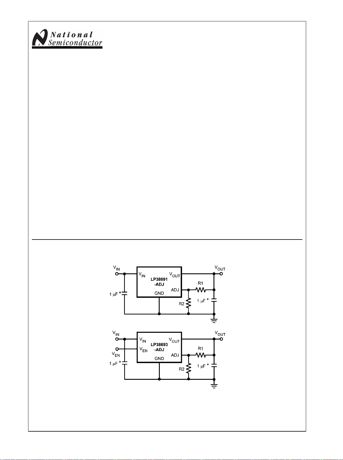
Typical Application Circuits
Features
Output voltage range of 1.25V - 9V
■
2.0% adjust pin voltage accuracy (25°C)
■
Low dropout voltage: 250mV @ 500mA (typ, 5V out)
■
Wide input voltage range (2.7V to 10V)
■
Precision (trimmed) bandgap reference
■
Guaranteed specs for -40°C to +125°C
■
1µA off-state quiescent current
■
Thermal overload protection
■
Foldback current limiting
■
SOT-223 and 6-Lead LLP packages
■
Enable pin (LP38693-ADJ)
■
Applications
Hard Disk Drives
■
Notebook Computers
■
Battery Powered Devices
■
Portable Instrumentation
■
20126801
20126802
V
= V
OUT
Note:
*Minimum value required for stability.
© 2008 National Semiconductor Corporation 201268 www.national.com
x (1 + R1/R2)
ADJ
Page 2
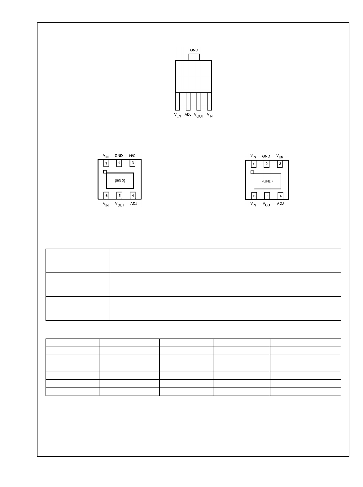
Connection Diagrams
LP38691-ADJ/LP38693-ADJ
6-Lead LLP, Bottom View
LP38691SD-ADJ
Pin Descriptions
Pin Description
V
IN
GND Circuit ground for the regulator. This is connected to the die through the lead frame, and also functions
V
OUT
V
EN
ADJ The adjust pin is used to set the regulated output voltage by connecting it to the external resistors
SOT-223, Top View
20126803
LP38693MP-ADJ
20126804
6-Lead LLP, Bottom View
20126805
LP38693SD-ADJ
This is the input supply voltage to the regulator. For LLP package devices, both VIN pins must be tied
together for full current operation (250mA maximum per pin).
as the heat sink when the large ground pad is soldered down to a copper plane.
Regulated output voltage.
The enable pin allows the part to be turned ON and OFF by pulling this pin high or low.
R1 and R2 (see Typical Application Circuit).
Ordering Information
Order Number Package Marking Package Type Package Drawing Supplied As
LP38691SD-ADJ L117B 6-Lead LLP SDE06A 1000 Units Tape and Reel
LP38693SD-ADJ L127B 6-Lead LLP SDE06A 1000 Units Tape and Reel
LP38693MP-ADJ LJUB SOT-223 MP05A 1000 Units Tape and Reel
LP38691SDX-ADJ L117B 6-Lead LLP SDE06A 4500 Units Tape and Reel
LP38693SDX-ADJ L127B 6-Lead LLP SDE06A 4500 Units Tape and Reel
LP38693MPX-ADJ LJUB SOT-223 MP05A 2000 Units Tape and Reel
www.national.com 2
Page 3
LP38691-ADJ/LP38693-ADJ
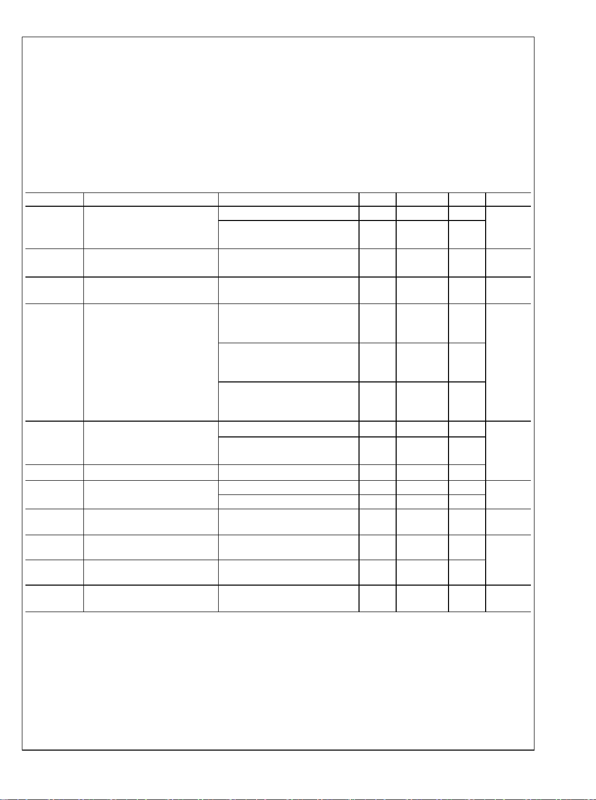
Absolute Maximum Ratings (Note 1)
If Military/Aerospace specified devices are required,
please contact the National Semiconductor Sales Office/
V(max) All pins (with respect to GND) -0.3V to 12V
I
OUT
Junction Temperature −40°C to +150°C
Distributors for availability and specifications.
Storage Temperature Range −65°C to +150°C
Lead Temp. (Soldering, 5 seconds) 260°C
ESD Rating (Note 3) 2 kV
Power Dissipation (Note 2) Internally Limited
Electrical Characteristics Limits in standard typeface are for T
the full operating temperature range. Unless otherwise specified: VIN = V
Operating Ratings
VIN Supply Voltage 2.7V to 10V
Operating Junction
Temperature Range
= 25°C, and limits in boldface type apply over
J
+ 1V, CIN = C
OUT
limits are guaranteed through testing, statistical correlation, or design.
Symbol Parameter Conditions Min
VIN = 2.7V
V
ADJ
ADJ Pin Voltage
3.2V ≤ VIN ≤ 10V
100 µA < IL < 0.5A
ΔVO/ΔV
ΔVO/ΔI
L
Output Voltage Line Regulation
IN
(Note 6)
Output Voltage Load Regulation
(Note 7)
VO + 0.5V ≤ VIN ≤ 10V
IL = 25mA
1 mA < IL < 0.5A
VIN = VO + 1V
(VO = 2.5V)
IL = 0.1A
IL = 0.5A
(VO = 3.3V)
VIN - V
O
Dropout Voltage (Note 8)
IL = 0.1A
IL = 0.5A
(VO = 5V)
IL = 0.1A
IL = 0.5A
I
Q
Quiescent Current
VIN ≤ 10V, IL = 100 µA - 0.5A
VEN ≤ 0.4V,
(LP38693-ADJ Only)
IL(MIN) Minimum Load Current
I
FB
Foldback Current Limit VIN - VO > 5V
VIN - VO ≤ 4V
VIN - VO < 4V 850
PSRR Ripple Rejection VIN = VO + 2V(DC), with 1V(p-p) /
120Hz Ripple
T
SD
Thermal Shutdown Activation
(Junction Temp)
TSD (HYST) Thermal Shutdown Hysteresis
(Junction Temp)
I
ADJ
ADJ Input Leakage Current V
= 0 - 1.5V
ADJ
VIN = 10V
Internally Limited
−40°C to +125°C
= 10 µF, I
OUT
Typ (Note 4)
= 10mA. Min/Max
LOAD
Max Units
1.225 1.25 1.275
1.200 1.25 1.300
0.03 0.1 %/V
1.8 5 %/A
80
430
65
330
45
250
145
725
110
550
100
450
55 100
0.001 1
100
350
55 dB
160
10
-100 0.01 100 nA
V
mV
µA
mA
°C
3 www.national.com
Page 4
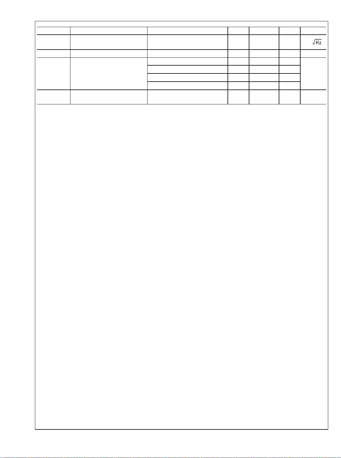
Symbol Parameter Conditions Min
e
n
Output Noise BW = 10Hz to 10kHz
VO = 3.3V
VO (LEAK) Output Leakage Current VO = VO(NOM) + 1V @ VIN = 10V
V
EN
Enable Voltage (LP38693-ADJ
Only)
Output = OFF 0.4
Output = ON, VIN = 4V 1.8
Typ (Note 4)
0.7
0.5 2 µA
Max Units
Output = ON, VIN = 6V 3.0
Output = ON, VIN = 10V 4.0
I
EN
LP38691-ADJ/LP38693-ADJ
Note 1: Absolute maximum ratings indicate limits beyond which damage to the component may occur. Operating ratings indicate conditions for which the device
is intended to be functional, but do not guarantee specific performance limits. For guaranteed specifications, see Electrical Characteristics. Specifications do not
apply when operating the device outside of its rated operating conditions.
Note 2: At elevated temperatures, device power dissipation must be derated based on package thermal resistance and heatsink values (if a heatsink is used).
The junction-to-ambient thermal resistance (θ
copper area (less than 0.1 square inch). If one square inch of copper is used as a heat dissipator for the SOT-223, the θ
θ
values for the LLP package are also dependent on trace area, copper thickness, and the number of thermal vias used (refer to application note AN-1187). If
J-A
power disspation causes the junction temperature to exceed specified limits, the device will go into thermal shutdown.
Note 3: ESD is tested using the human body model which is a 100pF capacitor discharged through a 1.5k resistor into each pin.
Note 4: Typical numbers represent the most likely parametric norm for 25°C operation.
Note 5: If used in a dual-supply system where the regulator load is returned to a negative supply, the output pin must be diode clamped to ground.
Note 6: Output voltage line regulation is defined as the change in output voltage from nominal value resulting from a change in input voltage.
Note 7: Output voltage load regulation is defined as the change in output voltage from nominal value as the load current increases from 1mA to full load.
Note 8: Dropout voltage is defined as the minimum input to output differential required to maintain the output within 100mV of nominal value.
Enable Pin Leakage (LP38693ADJ Only)
) for the SOT-223 is approximately 125 °C/W for a PC board mounting with the device soldered down to minimum
J-A
VEN = 0V or 10V, VIN = 10V -1 0.001 1
drops to approximately 70 °C/W. The
J-A
µV/
V
µA
www.national.com 4
Page 5
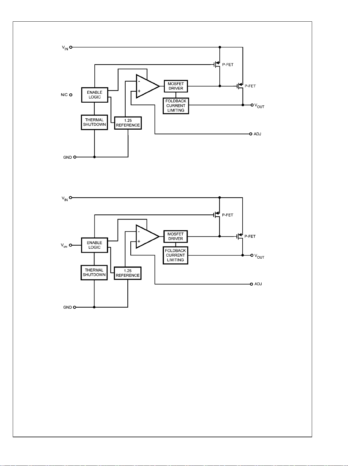
Block Diagrams
LP38691-ADJ/LP38693-ADJ
20126806
FIGURE 1. LP38691-ADJ Functional Diagram (LLP)
FIGURE 2. LP38693-ADJ Functional Diagram (SOT-223, LLP)
5 www.national.com
20126807
Page 6

Typical Performance Characteristics Unless otherwise specified: T
pin is tied to VIN (LP38693-ADJ only), VO = 1.25V, VIN = 2.7V, IL = 10mA.
= 25°C, CIN = C
J
= 10 µF, enable
OUT
Noise vs Frequency
LP38691-ADJ/LP38693-ADJ
Noise vs Frequency
20126835
Noise vs Frequency
20126836
Ripple Rejection
20126837
Ripple Rejection
20126819
www.national.com 6
20126817
Ripple Rejection
20126821
Page 7

V
vs Temperature
REF
LP38691-ADJ/LP38693-ADJ
Line Transient Response
20126823
20126830
Line Transient Response
Line Transient Response
20126824
Line Transient Response
20126825
Line Transient Response
20126826
20126827
7 www.national.com
Page 8

Line Transient Response
LP38691-ADJ/LP38693-ADJ
Load Transient Response
Load Transient Response
Load Regulation vs Temperature
20126828
20126844
20126842
Enable Voltage vs Temperature
20126853
Line Regulation vs Temperature
20126854
www.national.com 8
20126855
Page 9

V
OUT
vs VIN , V
OUT
= 1.25V
V
OUT
vs VIN , V
OUT
LP38691-ADJ/LP38693-ADJ
= 1.80V
MIN VIN vs I
OUT
20126858
20126856
Dropout Voltage vs I
(V
= 1.8V)
OUT
20126859
OUT
20126857
9 www.national.com
Page 10

Application Hints
EXTERNAL CAPACITORS
Like any low-dropout regulator, external capacitors are required to assure stability. These capacitors must be correctly
selected for proper performance.
INPUT CAPACITOR: An input capacitor of at least 1µF is required (ceramic recommended). The capacitor must be located not more than one centimeter from the input pin and
returned to a clean analog ground.
OUTPUT CAPACITOR: An output capacitor is required for
loop stability. It must be located less than 1 centimeter from
LP38691-ADJ/LP38693-ADJ
the device and connected directly to the output and ground
pins using traces which have no other currents flowing
through them.
The minimum amount of output capacitance that can be used
for stable operation is 1µF. Ceramic capacitors are recommended (the LP38691/3-ADJ was designed for use with ultra
low ESR capacitors). The LP38691/3-ADJ is stable with any
output capacitor ESR between zero and 100 Ohms.
SETTING THE OUTPUT VOLTAGE: The output voltage is
set using the external resistors R1 and R2 (see Typical Application Circuit). The output voltage will be given by the
equation:
V
= V
OUT
Because the part has a minimum load current requirement of
100 µA, it is recommended that R2 always be 12k Ohms or
less to provide adequate loading. Even if a minimum load is
always provided by other means, it is not recommended that
very high value resistors be used for R1 and R2 because it
can make the ADJ node susceptible to noise pickup. A maximum Ohmic value of 100k is recommended for R2 to prevent
this from occurring.
ENABLE PIN (LP38693-ADJ only): The LP38693-ADJ has
an enable pin which turns the regulator output on and off.
Pulling the enable pin down to a logic low will turn the part off.
The voltage the pin has to be pulled up to in order to assure
the part is on depends on input voltage (refer to Electrical
Characteristics section). This pin should be tied to VIN if the
enable function is not used.
FOLDBACK CURRENT LIMITING: Foldback current limiting
is built into the LP38691/3-ADJ which reduces the amount of
output current the part can deliver as the output voltage is
reduced. The amount of load current is dependent on the differential voltage between VIN and V
differential voltage exceeds 5V, the load current will limit at
about 350 mA. When the VIN -V
low 4V, load current is limited to about 850 mA.
SELECTING A CAPACITOR
It is important to note that capacitance tolerance and variation
with temperature must be taken into consideration when selecting a capacitor so that the minimum required amount of
capacitance is provided over the full operating temperature
range.
Capacitor Characteristics
CERAMIC: For values of capacitance in the 10 to 100 µF
range, ceramics are usually larger and more costly than tantalums but give superior AC performance for bypassing high
frequency noise because of very low ESR (typically less than
10 mΩ). However, some dielectric types do not have good
capacitance characteristics as a function of voltage and temperature.
X (1 + R1/R2)
ADJ
differential is reduced be-
OUT
. Typically, when this
OUT
Z5U and Y5V dielectric ceramics have capacitance that drops
severely with applied voltage. A typical Z5U or Y5V capacitor
can lose 60% of its rated capacitance with half of the rated
voltage applied to it. The Z5U and Y5V also exhibit a severe
temperature effect, losing more than 50% of nominal capacitance at high and low limits of the temperature range.
X7R and X5R dielectric ceramic capacitors are strongly recommended if ceramics are used, as they typically maintain a
capacitance range within ±20% of nominal over full operating
ratings of temperature and voltage. Of course, they are typically larger and more costly than Z5U/Y5U types for a given
voltage and capacitance.
TANTALUM: Solid Tantalum capacitors have good temperature stability: a high quality Tantalum will typically show a
capacitance value that varies less than 10-15% across the full
temperature range of -40°C to 125°C. ESR will vary only
about 2X going from the high to low temperature limits.
The increasing ESR at lower temperatures can cause oscillations when marginal quality capacitors are used (if the ESR
of the capacitor is near the upper limit of the stability range at
room temperature).
PCB LAYOUT
Good PC layout practices must be used or instability can be
induced because of ground loops and voltage drops. The input and output capacitors must be directly connected to the
input, output, and ground pins of the regulator using traces
which do not have other currents flowing in them (Kelvin connect).
The best way to do this is to lay out CIN and C
device with short traces to the VIN, V
regulator ground pin should be connected to the external cir-
, and ground pins. The
OUT
near the
OUT
cuit ground so that the regulator and its capacitors have a
"single point ground".
It should be noted that stability problems have been seen in
applications where "vias" to an internal ground plane were
used at the ground points of the IC and the input and output
capacitors. This was caused by varying ground potentials at
these nodes resulting from current flowing through the ground
plane. Using a single point ground technique for the regulator
and it’s capacitors fixed the problem. Since high current flows
through the traces going into VIN and coming from V
Kelvin connect the capacitor leads to these pins so there is
OUT
no voltage drop in series with the input and output capacitors.
RFI/EMI SUSCEPTIBILITY
RFI (radio frequency interference) and EMI (electromagnetic
interference) can degrade any integrated circuit’s performance because of the small dimensions of the geometries
inside the device. In applications where circuit sources are
present which generate signals with significant high frequency energy content (> 1 MHz), care must be taken to ensure
that this does not affect the IC regulator.
If RFI/EMI noise is present on the input side of the regulator
(such as applications where the input source comes from the
output of a switching regulator), good ceramic bypass capacitors must be used at the input pin of the IC.
If a load is connected to the IC output which switches at high
speed (such as a clock), the high-frequency current pulses
required by the load must be supplied by the capacitors on
the IC output. Since the bandwidth of the regulator loop is less
than 100 kHz, the control circuitry cannot respond to load
changes above that frequency. This means the effective output impedance of the IC at frequencies above 100 kHz is
determined only by the output capacitor(s).
,
www.national.com 10
Page 11

LP38691-ADJ/LP38693-ADJ
In applications where the load is switching at high speed, the
output of the IC may need RF isolation from the load. It is
recommended that some inductance be placed between the
output capacitor and the load, and good RF bypass capacitors
be placed directly across the load.
PCB layout is also critical in high noise environments, since
RFI/EMI is easily radiated directly into PC traces. Noisy circuitry should be isolated from "clean" circuits where possible,
and grounded through a separate path. At MHz frequencies,
ground planes begin to look inductive and RFI/ EMI can cause
ground bounce across the ground plane. In multi-layer PCB
applications, care should be taken in layout so that noisy
power and ground planes do not radiate directly into adjacent
layers which carry analog power and ground.
OUTPUT NOISE Noise is specified in two ways- Spot Noise or Output
Noise density is the RMS sum of all noise sources, measured
at the regulator output, at a specific frequency (measured with
a 1Hz bandwidth). This type of noise is usually plotted on a
curve as a function of frequency. Total Output Noise or
Broad-Band Noise is the RMS sum of spot noise over a
specified bandwidth, usually several decades of frequencies.
Attention should be paid to the units of measurement. Spot
noise is measured in units µV/root-Hz or nV/root-Hz and total
output noise is measured in µV(rms)
The primary source of noise in low-dropout regulators is the
internal reference. Noise can be reduced in two ways: by increasing the transistor area or by increasing the current drawn
by the internal reference. Increasing the area will decrease
the chance of fitting the die into a smaller package. Increasing
the current drawn by the internal reference increases the total
supply current (ground pin current).
11 www.national.com
Page 12

Physical Dimensions inches (millimeters) unless otherwise noted
LP38691-ADJ/LP38693-ADJ
6-lead, LLP Package
NS Package Number SDE06A
SOT-223 Package
NS Package Number MP05A
www.national.com 12
Page 13

Notes
LP38691-ADJ/LP38693-ADJ
13 www.national.com
Page 14

Notes
For more National Semiconductor product information and proven design tools, visit the following Web sites at:
Products Design Support
Amplifiers www.national.com/amplifiers WEBENCH www.national.com/webench
Audio www.national.com/audio Analog University www.national.com/AU
Clock Conditioners www.national.com/timing App Notes www.national.com/appnotes
Data Converters www.national.com/adc Distributors www.national.com/contacts
Displays www.national.com/displays Green Compliance www.national.com/quality/green
Ethernet www.national.com/ethernet Packaging www.national.com/packaging
Interface www.national.com/interface Quality and Reliability www.national.com/quality
LVDS www.national.com/lvds Reference Designs www.national.com/refdesigns
Power Management www.national.com/power Feedback www.national.com/feedback
Switching Regulators www.national.com/switchers
LDOs www.national.com/ldo
LED Lighting www.national.com/led
PowerWise www.national.com/powerwise
Serial Digital Interface (SDI) www.national.com/sdi
Temperature Sensors www.national.com/tempsensors
Wireless (PLL/VCO) www.national.com/wireless
OutputStable with Ceramic Output Capacitors
THE CONTENTS OF THIS DOCUMENT ARE PROVIDED IN CONNECTION WITH NATIONAL SEMICONDUCTOR CORPORATION
(“NATIONAL”) PRODUCTS. NATIONAL MAKES NO REPRESENTATIONS OR WARRANTIES WITH RESPECT TO THE ACCURACY
OR COMPLETENESS OF THE CONTENTS OF THIS PUBLICATION AND RESERVES THE RIGHT TO MAKE CHANGES TO
SPECIFICATIONS AND PRODUCT DESCRIPTIONS AT ANY TIME WITHOUT NOTICE. NO LICENSE, WHETHER EXPRESS,
IMPLIED, ARISING BY ESTOPPEL OR OTHERWISE, TO ANY INTELLECTUAL PROPERTY RIGHTS IS GRANTED BY THIS
DOCUMENT.
TESTING AND OTHER QUALITY CONTROLS ARE USED TO THE EXTENT NATIONAL DEEMS NECESSARY TO SUPPORT
NATIONAL’S PRODUCT WARRANTY. EXCEPT WHERE MANDATED BY GOVERNMENT REQUIREMENTS, TESTING OF ALL
PARAMETERS OF EACH PRODUCT IS NOT NECESSARILY PERFORMED. NATIONAL ASSUMES NO LIABILITY FOR
APPLICATIONS ASSISTANCE OR BUYER PRODUCT DESIGN. BUYERS ARE RESPONSIBLE FOR THEIR PRODUCTS AND
APPLICATIONS USING NATIONAL COMPONENTS. PRIOR TO USING OR DISTRIBUTING ANY PRODUCTS THAT INCLUDE
NATIONAL COMPONENTS, BUYERS SHOULD PROVIDE ADEQUATE DESIGN, TESTING AND OPERATING SAFEGUARDS.
EXCEPT AS PROVIDED IN NATIONAL’S TERMS AND CONDITIONS OF SALE FOR SUCH PRODUCTS, NATIONAL ASSUMES NO
LIABILITY WHATSOEVER, AND NATIONAL DISCLAIMS ANY EXPRESS OR IMPLIED WARRANTY RELATING TO THE SALE
AND/OR USE OF NATIONAL PRODUCTS INCLUDING LIABILITY OR WARRANTIES RELATING TO FITNESS FOR A PARTICULAR
PURPOSE, MERCHANTABILITY, OR INFRINGEMENT OF ANY PATENT, COPYRIGHT OR OTHER INTELLECTUAL PROPERTY
RIGHT.
LIFE SUPPORT POLICY
NATIONAL’S PRODUCTS ARE NOT AUTHORIZED FOR USE AS CRITICAL COMPONENTS IN LIFE SUPPORT DEVICES OR
SYSTEMS WITHOUT THE EXPRESS PRIOR WRITTEN APPROVAL OF THE CHIEF EXECUTIVE OFFICER AND GENERAL
COUNSEL OF NATIONAL SEMICONDUCTOR CORPORATION. As used herein:
Life support devices or systems are devices which (a) are intended for surgical implant into the body, or (b) support or sustain life and
whose failure to perform when properly used in accordance with instructions for use provided in the labeling can be reasonably expected
to result in a significant injury to the user. A critical component is any component in a life support device or system whose failure to perform
can be reasonably expected to cause the failure of the life support device or system or to affect its safety or effectiveness.
National Semiconductor and the National Semiconductor logo are registered trademarks of National Semiconductor Corporation. All other
brand or product names may be trademarks or registered trademarks of their respective holders.
Copyright© 2008 National Semiconductor Corporation
For the most current product information visit us at www.national.com
LP38691-ADJ/LP38693-ADJ 500mA Low Dropout CMOS Linear Regulators with Adjustable
www.national.com
National Semiconductor
Americas Technical
Support Center
Email: support@nsc.com
Tel: 1-800-272-9959
National Semiconductor Europe
Technical Support Center
Email: europe.support@nsc.com
German Tel: +49 (0) 180 5010 771
English Tel: +44 (0) 870 850 4288
National Semiconductor Asia
Pacific Technical Support Center
Email: ap.support@nsc.com
National Semiconductor Japan
Technical Support Center
Email: jpn.feedback@nsc.com
 Loading...