

Page 1
TL/H/5023
LP265/LP365 Micropower Programmable Quad Comparator
December 1994
LP265/LP365 Micropower Programmable
Quad Comparator
General Description
The LP365 consists of four independent voltage comparators. The comparators can be programmed, four at the
same time, for various supply currents, input currents, response times and output current drives. This is accomplished by connecting a single resistor between the V
CC
and I
SET
pins.
These comparators can be operated from split power supplies or from a single power supply over a wide range of
voltages. The input can sense signals at ground level even
with single supply operation. The unique output NPN transistor stages are uncommitted to either power supply. They
can be connected directly to various logic system supplies
so that they are highly flexible to interface with various logic
families.
Application areas include battery power circuits, threshold
detectors, zero crossing detectors, simple serial A/D converters, VCO, multivibrators, voltage converters, power sequencers, and high performance V/F converters, and RTD
linearization.
Features
Y
Single programming resistor to tailor power consumption, input current, speed and output current drive
capability
Y
Wide single supply voltage range or dual supplies (4
V
DC
to 36 VDCorg2.0 VDCtog18 VDC)
Y
Low supply current drain (10 mA) and low power
consumption (10 mW/comparator)
@
I
SET
e
0.5 mA
V
CC
e
5
VDC
Y
Uncommitted output stageÐselectable output levels
Y
Output directly compatible with DTL, TTL, CMOS, MOS
or other special logic families
Y
Input common-mode range includes ground
Y
Differential input voltage equal to the power supply
voltage
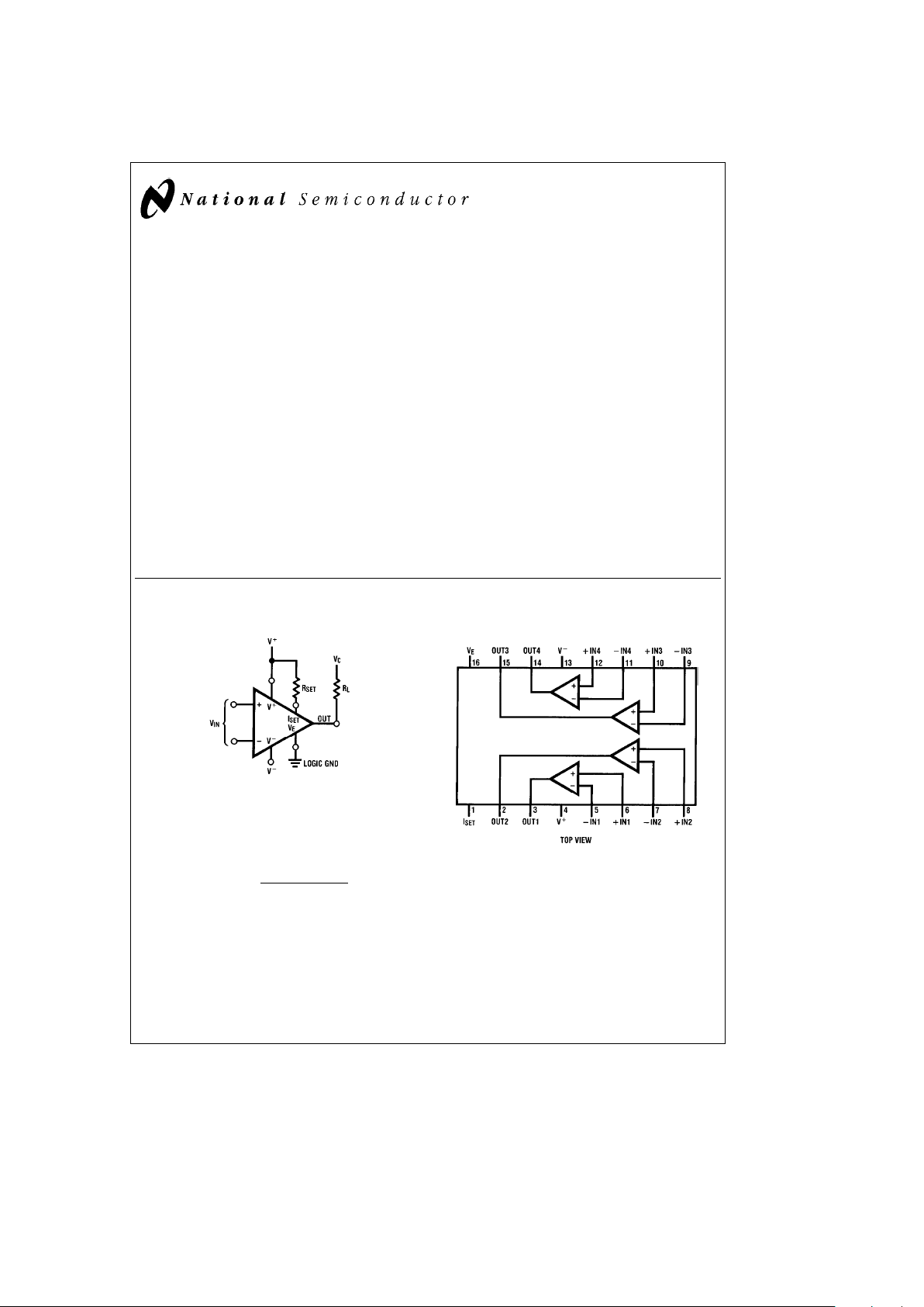
Typical Connection
TL/H/5023– 1
Programming Equation
I
SET
e
(Va)b(Vb)b1.3V
R
SET
I
SUPPLY
&
22
c
I
SET
Connection Diagram
Dual-In-Line Package
TL/H/5023– 2
Order Number LP365M, LP365AN or LP365N
See NS Package Numbers M16A or N16A
C
1995 National Semiconductor Corporation RRD-B30M115/Printed in U. S. A.
Page 2

Absolute Maximum Ratings
If Military/Aerospace specified devices are required,
please contact the National Semiconductor Sales
Office/Distributors for availability and specifications.
Supply Voltage 36 V
DC
org18 V
DC
Differential Input Voltage
g
36 V
DC
Input Voltage (Note 1)
b
0.3V toa36 V
DC
Output Short Circuit to VE(Note 2) Continuous
V
OUT
with Respect to V
E
V
E
b
7VsV
OUT
s
V
E
a
36V
ESD Tolerance (Note 10) 2000V
M Package N Package
Power Dissipation (Note 3) 500 mW 500 mW
T
j
Max 115§C 115§C
i
jA
115§C/W 90§C/W
Lead Temp.
(SolderingÐ10 sec.) 260
§
C
(Vapor PhaseÐ60 sec.) 215
§
C
(InfraredÐ15 sec.) 220
§
C
Operating Temp. Range LP365: 0
§
CsT
A
s
a
70§C
Storage Temp. Range
b
40§CsT
A
s
a
150§C
Electrical Characteristics (Note 4) Low power V
S
e
5V, I
SET
e
10 mA
LP365A LP365
Symbol Parameter Conditions
Tested Design Tested Design Units
Typ Limit Limit Typ Limit Limit (Limit)
(Note 5) (Note 6) (Note 5) (Note 6)
V
OS
Input Offset V
CM
e
OV,
13 636 9
mV
Voltage R
S
e
100 (Max)
I
OS
Input Offset V
CM
e
0V 2 20 50 425 75
nA
Current LP265
425 150
(Max)
I
B
Input Bias V
CM
e
0V 10 50 125 15 75 200
nA
Current LP265
15 75 300
(Max)
A
VOL
Large Signal R
L
e
100k
500 50 50 300 25 25
V/mV
Voltage Gain (Min)
V
CM
Input Common-
0 0 0 0
V
Mode Voltage (Max)
Range
3 3 3 3
V
(Min)
CMRR Common-Mode 0sV
CM
s
3V
85 75 70 80 75 70
dB
Rejection Ratio (Min)
PSRR Supply Voltage
g
2.5VsV
S
75 65 65 70 65
65 dB
Rejection Ratio
s
g
3.5V (Min)
I
S
Supply Current All Inputse0V,
215 250 300 225 275 300
mA
R
L
e %
(Max)
V
OH
Output Voltage V
C
e
5V,
V
High V
E
e
0V, 4.9 4.5 4.9 4.5
(Min)
R
L
e
100k
V
OL
Output Voltage V
E
e
0V
0.4
0.4
0.4 0.4
V
Low (Max)
I
SINK
Output Sink V
E
e
0V,
2.4 1.2 0.6 2.0 0.8 0.4
mA
Current V
O
e
0.4V (Min)
I
LEAK
Output Leakage V
C
e
5V,
2505000 2 100 5000
nA
Current V
E
e
0V (Max)
t
R
Response Time V
CC
e
5V,
V
E
e
0V,
R
L
e
5k, 4 4 ms
C
L
e
10 pF
(Note 7)
2
Page 3

Electrical Characteristics (Continued) (Note 8) High power V
S
e
g
15V, I
SET
e
100 mA
LP365A LP365
Symbol Parameter Conditions
Tested Design Tested Design
Units
Typ Limit Limit Typ Limit Limit
(Limit)
(Note 5) (Note 6) (Note 5) (Note 6)
V
OS
Input Offset V
CM
e
0V,
13 636 9
mV
Voltage R
S
e
100 (Max)
I
OS
Input Offset V
CM
e
0V 5 50 100 10 90 200
nA
Current LP265
10 90 500
(Max)
I
B
Input Bias V
CM
e
0V 60 200 500 80 300 500
nA
Current LP265
80 300 800
(Max)
A
VOL
Large Signal R
L
e
15k
500 100 100 500 100 100
V/mV
Voltage Gain (Min)
V
CM
Input Common-
b
15
b
15
b
15
b
15
V
Mode Voltage (Max)
Range
13 13 13 13
V
(Min)
CMRR Common-Mode
b
15VsV
CM
85 75 70 80 75 70
dB
Rejection Ratio
s
13V (Min)
PSRR Supply Voltage
g
10VsV
S
80 70 70 75 70 70
dB
Rejection Ratio
s
g
15V (Min)
I
S
Supply Current All Inputse0V, 2.6 3 3.3 2.8 3.5 3.7
mA
R
L
e %
, LP265
2.8 3.5 4.3
(Max)
V
OH
Output Voltage V
C
e
5V,
V
High V
E
e
0V, 4.9 4.5 4.9 4.5
(Min)
R
L
e
100k
V
OL
Output Voltage V
E
e
0V
0.4 0.4 0.4 0.4
V
Low (Max)
I
SINK
Output Sink V
E
e
0V,
10 8 5.5 7.5 6 4
mA
Current V
O
e
0.4V (Min)
I
LEAK
Output Leakage V
C
e
15V,
5505000 5505000
nA
Current V
E
eb
15V (Max)
t
R
Response Time V
CC
e
5V,
V
E
e
0V,
R
L
e
5k, 1.0 1.0 ms
C
L
e
10 pF
(Note 7)
Note 1: The input voltage is not allowed to go 0.3V above Vaorb0.3V below Vbas this will turn on a parasitic transistor causing large currents to flow through
the device.
Note 2: Short circuits from the output to V
a
may cause excessive heating and eventual destruction. The current in the output leads and the VElead should not be
allowed to exceed 30 mA. The output should not be shorted to V
b
if V
E
s
(Vb)a7V.
Note 3: For operating at elevated temperatures, these devices must be derated based on a thermal resistance of i
jA
and Tjmax. T
j
e
T
A
a
ijAPD.
Note 4: Boldface numbers apply at temperature extremes. All other numbers apply at T
A
e
T
j
e
25§C. V
a
e
5V, V
b
e
0V, I
SET
e
10 mA, R
L
e
100k, and
V
C
e
5V as shown in the Typical Connection diagram.
Note 5: Guaranteed and 100% production tested.
Note 6: Guaranteed (but not 100% production tested) over the operating temperature and supply voltage ranges. These limits are not used to calculate out-going
quality levels.
Note 7: The response time specified is for a 100 mV input step with 5 mV overdrive.
Note 8: Boldface numbers apply at temperature extremes. All other numbers apply at T
A
e
T
j
e
25§C. V
a
ea
15V, V
b
eb
15V, I
SET
e
100 mA, R
L
e
100k, and
V
C
e
5V as shown in the Typical Connection diagram.
Note 9: See AN-450 ‘‘Surface Mounting Methods and Their Effect on Product Reliability’’ for other methods of soldering surface mount devices.
Note 10: Human body model, 1.5 kX in series with 100 pF.
3
Page 4

Typical Performance Characteristics
Supply Current vs I
SET
Supply Current vs Supply
Voltage
Supply Current vs
Temperature
Input Bias Current vs I
SET
Output Saturation Voltage Voltage Gain vs I
SET
Response Time
Negative Transition
Response Time
Positive Transition
Response Time
Negative Transition
Response Time
Positive Transition
TL/H/5023– 3
4
Page 5

Typical Applications
Gated 4-Phase Oscillator
TL/H/5023– 4
fe20 kHz
f
e
1
1.6#R
t
#
C
t
All four phases run when X is low. When X is high, oscillation stops and
power drain is zero.
‘‘Voting’’ Comparator
TL/H/5023– 5
If V
E
e
0.25V, then V
OUT
will be low if 1 of the 3 other outputs are low.
Choice of V
E
e
0.50V causes V
OUT
to be low if 2 of the 3 other outputs are
low; V
E
e
0.75V will cause V
OUT
to be low if all 3 other outputs are low.
5
Page 6

Typical Applications (Continued)
Ordinary Hysteresis
TL/H/5023– 6
It is a good practice to add a few millivolts of positive feedback to prevent
oscillation when the input voltage is near the threshold.
Hysteresis from Emitter
TL/H/5023– 7
Positive feedback from the emitter can also prevent oscillations when VINis
near the threshold.
Bar-Graph Display
TL/H/5023– 8
The positive feedback from pin 16 provides hysteresis.
Level-Sensitive Strobe
TL/H/5023– 9
Comparators B, C, and D do not respond until activated by the signal applied
to comparator A.
6
Page 7

Typical Applications (Continued)
Slow Op Amp (Inverter)
TL/H/5023– 10
R
B
e
Va/20 mA
Unlike most comparators, the LP365 can be used as an op amp, if suitable
R-C damping networks are used.
Slow Op Amp (Unity-Gain Follower)
TL/H/5023– 11
R
B
e
Va/20 mA
The LP365 can also be used as a high-input-impedance follower-amplifier
with the damping components shown.
Chopping Outputs
TL/H/5023– 12
Chopping the outputs by modulating the I
SET
current allows data to be trans-
mitted via opto-couplers, transformers, etc.
Low Battery Detector
TL/H/5023– 13
I
S
@
6Ve45 mA
I
S
@
3.8Ve1 mA
f
e
3 kHz
Comparator A detects when the supply voltage drops to 4V and enables
comparator B to drive a piezoelectric alarm.
7
Page 8

Simplified Schematic
TL/H/5023– 14
Current sources are programmed by I
SET
VEis common to all 4 comparators
8
Page 9

Physical Dimensions inches (millimeters)
Plastic Surface-Mount Package (M)
Order Number LP365M
NS Package Number M16A
9
Page 10

LP265/LP365 Micropower Programmable Quad Comparator
Physical Dimensions inches (millimeters) (Continued)
Molded Dual-In-Line Package (N)
Order Number LP365AN or LP365N
NS Package Number N16A
LIFE SUPPORT POLICY
NATIONAL’S PRODUCTS ARE NOT AUTHORIZED FOR USE AS CRITICAL COMPONENTS IN LIFE SUPPORT
DEVICES OR SYSTEMS WITHOUT THE EXPRESS WRITTEN APPROVAL OF THE PRESIDENT OF NATIONAL
SEMICONDUCTOR CORPORATION. As used herein:
1. Life support devices or systems are devices or 2. A critical component is any component of a life
systems which, (a) are intended for surgical implant support device or system whose failure to perform can
into the body, or (b) support or sustain life, and whose be reasonably expected to cause the failure of the life
failure to perform, when properly used in accordance support device or system, or to affect its safety or
with instructions for use provided in the labeling, can effectiveness.
be reasonably expected to result in a significant injury
to the user.
National Semiconductor National Semiconductor National Semiconductor National Semiconductor
Corporation Europe Hong Kong Ltd. Japan Ltd.
1111 West Bardin Road Fax: (
a
49) 0-180-530 85 86 13th Floor, Straight Block, Tel: 81-043-299-2309
Arlington, TX 76017 Email: cnjwge@tevm2.nsc.com Ocean Centre, 5 Canton Rd. Fax: 81-043-299-2408
Tel: 1(800) 272-9959 Deutsch Tel: (
a
49) 0-180-530 85 85 Tsimshatsui, Kowloon
Fax: 1(800) 737-7018 English Tel: (
a
49) 0-180-532 78 32 Hong Kong
Fran3ais Tel: (
a
49) 0-180-532 93 58 Tel: (852) 2737-1600
Italiano Tel: (
a
49) 0-180-534 16 80 Fax: (852) 2736-9960
National does not assume any responsibility for use of any circuitry described, no circuit patent licenses are implied and National reserves the right at any time without notice to change said circuitry and specifications.
 Loading...