

Page 1
查询LP3470供应商
LP3470
Tiny Power On Reset Circuit
General Description
The LP3470 is a micropower CMOS voltage supervisory circuit designed to monitor power supplies in microprocessor
(µP) and other digital systems. It provides maximum adjustability forpower-on-reset(POR) and supervisory functions. It
is available in the following six standard reset threshold voltage (V
RTH
4.63V. If other voltage options between 2.4V and 5.0V are
desired please contact your National Semiconductor representative.
The LP3470 asserts a reset signal whenever the V
voltage falls below a reset threshold. The reset time-out period is adjustable using an external capacitor. Reset remains
asserted for an interval (programmed by an external capacitor) after V
The device is available in the tiny SOT23-5 package.
Key Specifications
±
n
1%Reset Threshold Accuracy Over Temperature
n Standard Reset Threshold Voltages: 2.63V, 2.93V,
3.08V, 4.00V, 4.38V, and 4.63V
) options: 2.63V, 2.93V, 3.08V, 4.00V, 4.38V, and
supply
CC
has risen above the threshold voltage.
CC
June 1999
n Custom Reset Threshold Voltages: For other voltages
between 2.4V and 5.0V contact your National
Semiconductor representative
n Very Low Quiescent Current (16 µA typical)
n Guaranteed Reset valid down to V
CC
=0.5V
Features
n Tiny SOT23-5 Package
n Open Drain Reset Output
n Programmable Reset Timeout Period Using an External
Capacitor
n Immune to Short V
Transients
CC
Applications
n Critical µP and µC Power Monitoring
n Intelligent Instruments
n Computers
n Portable/Battery-Powered Equipments
LP3470 Tiny Power On Reset Circuit
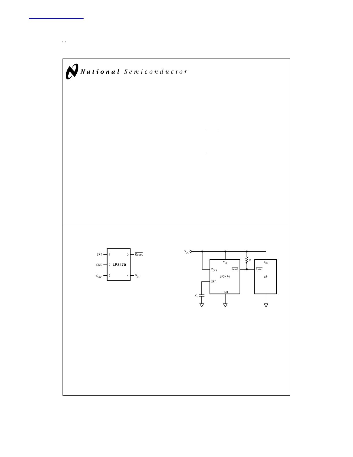
Pin Configuration and Basic Operating Circuit
Pin Configuration
DS100016-2
Top View
See NS Package Number
MA05B
Basic Operating Circuit
DS100016-1
© 1999 National Semiconductor Corporation DS100016 www.national.com
Page 2
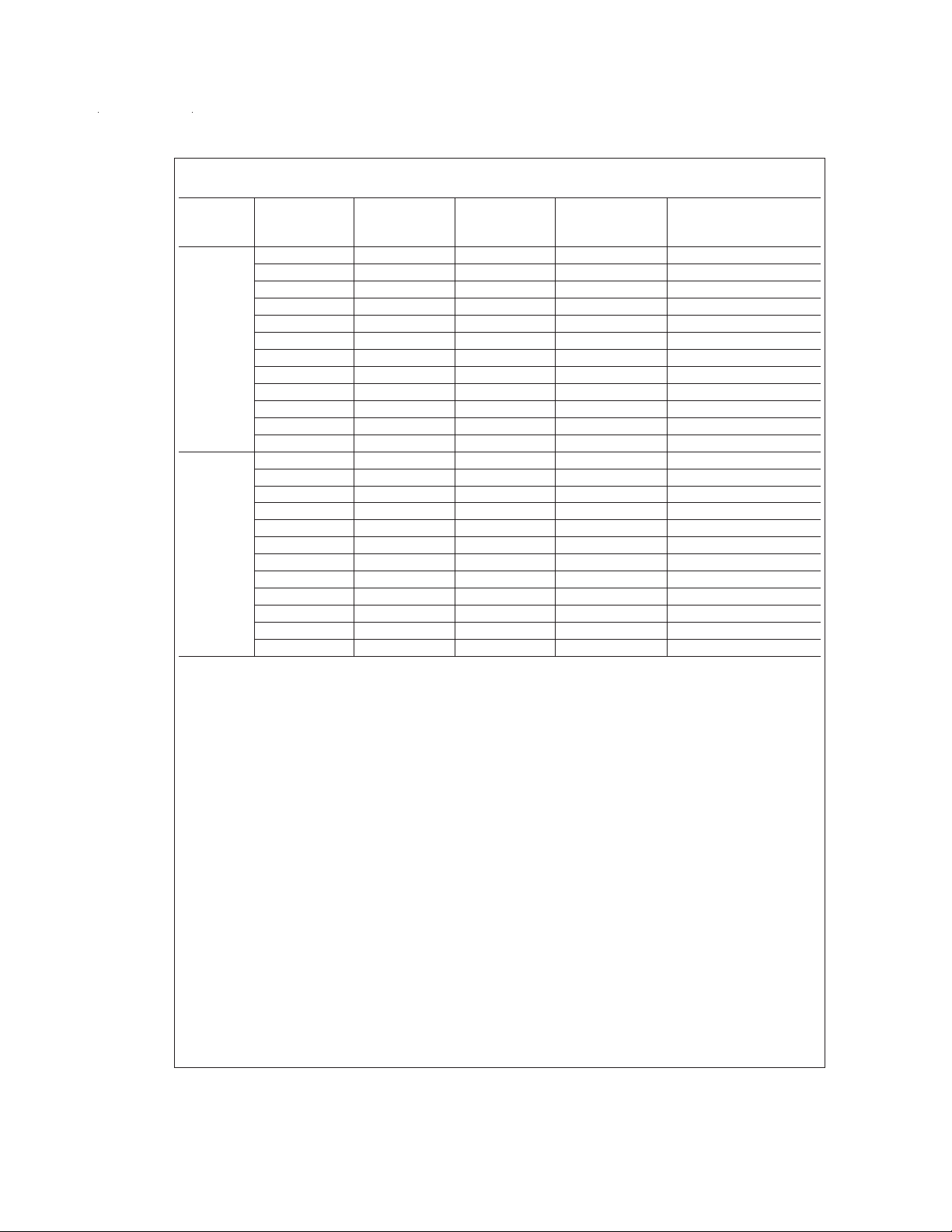
Ordering Information
Operating
Temperature
Range
−20˚C to
+85˚C
−40˚C to
+85˚C
Order
Number
LP3470M5-2.63 2.63 D25B SOT23-5 250 Units on Tape and Reel
LP3470M5X-2.63 2.63 D25B SOT23-5 3k Units on Tape and Reel
LP3470M5-2.93 2.93 D26B SOT23-5 250 Units on Tape and Reel
LP3470M5X-2.93 2.93 D26B SOT23-5 3k Units on Tape and Reel
LP3470M5-3.08 3.08 D28B SOT23-5 250 Units on Tape and Reel
LP3470M5X-3.08 3.08 D28B SOT23-5 3k Units on Tape and Reel
LP3470M5-4.00 4.00 D29B SOT23-5 250 Units on Tape and Reel
LP3470M5X-4.00 4.00 D29B SOT23-5 3k Units on Tape and Reel
LP3470M5-4.38 4.38 D30B SOT23-5 250 Units on Tape and Reel
LP3470M5X-4.38 4.38 D30B SOT23-5 3k Units on Tape and Reel
LP3470M5-4.63 4.63 D31B SOT23-5 250 Units on Tape and Reel
LP3470M5X-4.63 4.63 D31B SOT23-5 3k Units on Tape and Reel
LP3470IM5-2.63 2.63 D25C SOT23-5 250 Units on Tape and Reel
LP3470IM5X-2.63 2.63 D25C SOT23-5 3k Units on Tape and Reel
LP3470IM5-2.93 2.93 D26C SOT23-5 250 Units on Tape and Reel
LP3470IM5X-2.93 2.93 D26C SOT23-5 3k Units on Tape and Reel
LP3470IM5-3.08 3.08 D28C SOT23-5 250 Units on Tape and Reel
LP3470IM5X-3.08 3.08 D28C SOT23-5 3k Units on Tape and Reel
LP3470IM5-4.00 4.00 D29C SOT23-5 250 Units on Tape and Reel
LP3470IM5X-4.00 4.00 D29C SOT23-5 3k Units on Tape and Reel
LP3470IM5-4.38 4.38 D30C SOT23-5 250 Units on Tape and Reel
LP3470IM5X-4.38 4.38 D30C SOT23-5 3k Units on Tape and Reel
LP3470IM5-4.63 4.63 D31C SOT23-5 250 Units on Tape and Reel
LP3470IM5X-4.63 4.63 D31C SOT23-5 3k Units on Tape and Reel
Nominal
(V)
V
RTH
Package
Marking
Package
Type
Supplied As
www.national.com 2
Page 3
Absolute Maximum Ratings (Note 1)
If Military/Aerospace specified devices are required,
please contact the National Semiconductor Sales Office/
Distributors for availability and specifications.
V
Voltage −0.3V to +6V
CC
Reset Voltage
Output Current (Reset)
−0.3V to +6V
10 mA
Operating Temperature Range
LP3470 −20˚C to +85˚C
LP3470I −40˚C to +85˚C
Junction Temperature (T
Power Dissipation (T
2)
(Note 2) 280˚C/W
θ
JA
) 125˚C
Jmax
= 25˚C) (Note
A
300 mW
Storage Temp. Range −65˚C to +150˚C
Lead Temp. (Soldering, 5 sec) 260˚C
ESD Rating (Note 3) 2 kV
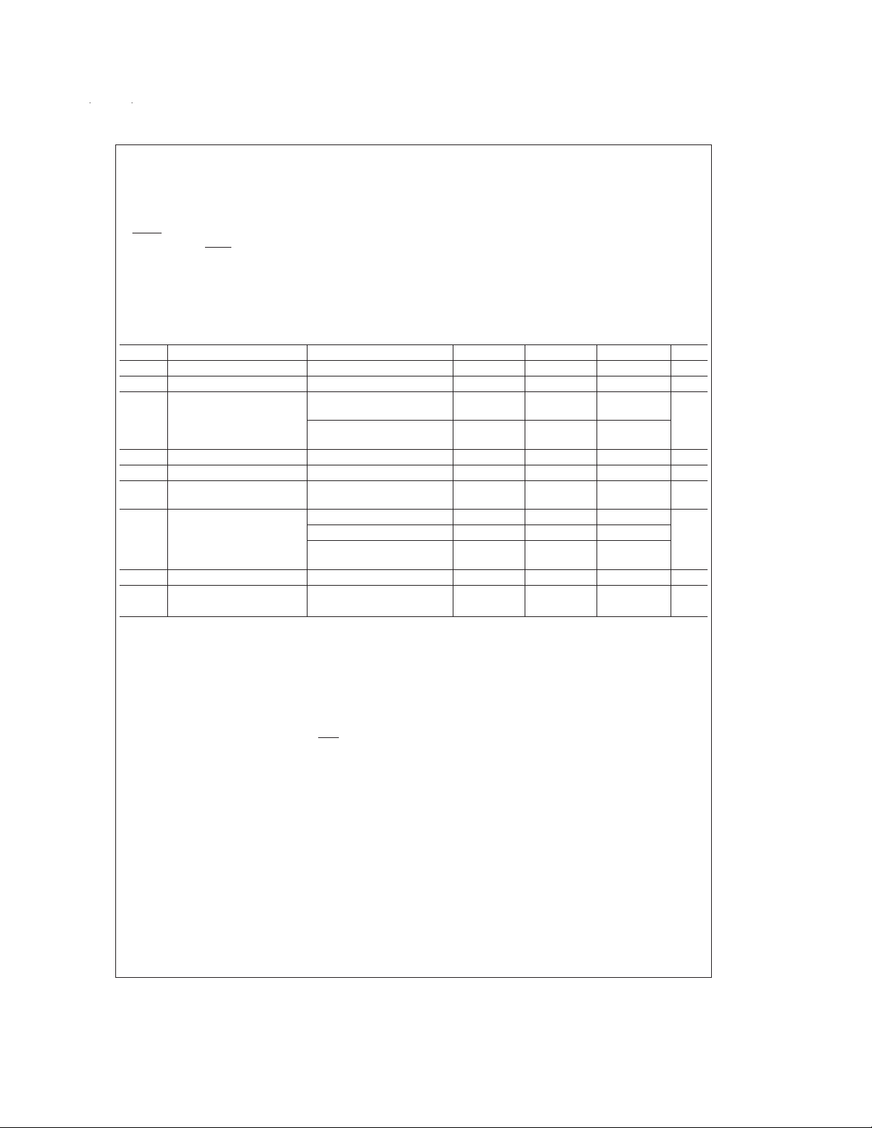
Electrical Characteristics
Limits in standard typeface are for TJ= 25˚C, and limits in boldface type apply over the full operating temperature range, unless
otherwise specified. VCC= +2.4V to +5.0V unless otherwise noted.
Symbol Parameter Conditions Typ (Note 4) Min (Note 5) Max (Note 5) Units
V
I
V
V
t
t
V
R
I
CC
CC
RTH
HYST
PD
RP
OL
1
LEAK
Operating Voltage Range 0.5 5.5 V
VCCSupply Current VCC= 4.5V 16 30 µA
Reset Threshold Voltage
(Note 6)
LP3470 V
LP3470I V
RTH
RTH
0.99 V
0.99 V
0.99 V
0.985 V
RTH
RTH
RTH
RTH
1.01 V
1.01 V
1.01 V
1.015 V
RTH
RTH
RTH
RTH
Hysteresis Voltage (Note 7) 35 15 65 mV
VCCto Reset Delay VCCfalling at 1 mV/µs 100 300 µs
Reset Timeout Period (Note8)C1=1nF 2 1.0 3.5
Reset Output Voltage Low VCC= 0.5V; IOL=30µA 0.1
= 1.0V; IOL= 100 µA 0.1
V
CC
V
CC=VRTH
mA
−100 mV; IOL=4
0.4
External Pull-up Resistor 20 0.68 68 kΩ
Reset Output Leakage
Current
Note 1: Absolute Maximum Ratings indicate limits beyond which damage to the device may occur. Electrical specifications do not apply when operating the device
beyond its operating conditions.
Note 2: The maximum power dissipation must be derated at elevated temperatures and is dictated by T
bient Thermal Resistance), and T
given in the Absolute Maximum Ratings, whichever is lower.
Note 3: The Human Body Model is a 100 pF capacitor discharged through a 1.5 kΩ resistor into each pin.
Note 4: Typical numbers are at 25˚C and represent the most likely parametric norm.
Note 5: Min. and Max. limits in standard typeface are 100%production tested at 25˚C. Min. and Max. limits in boldface are guaranteed through correlation using Sta-
tistical Quality Control (SQC) methods. The limits are used to calculate National’s Average Outgoing Quality Level (AOQL).
Note 6: Factory-trimmed reset thresholds are available in 50 mV increments from 2.4V to 5.0V. Contact your National Semiconductor representative.
Note 7: V
Note 8: tRPis programmable by varying the value of the external capacitor (C1) connected to pin SRT. The equation is: tRP=2000xC1(C1in µF and tRPin ms).
affects the relation between VCCand Reset as shown in the timing diagram.
HYST
(Ambient Temperature).Themaximum allowable power dissipation at any temperature is P
A
0.15 1
(Maximum Junction Temperature),θJA(Junction to Am-
Jmax
Dmax
=(T
Jmax−TA
)/ θJAor the number
6
V
ms
V
µA
www.national.com3
Page 4
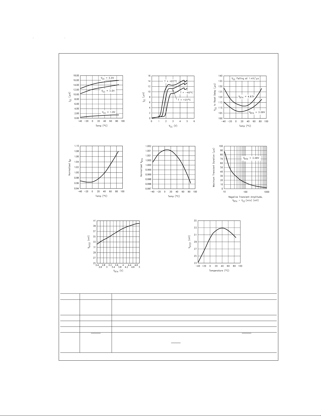
Typical Operating Characteristics T
I
vs Temperture
CC
ICCvs V
CC
= +25˚C, unless otherwise specified.
A
VCCto Reset Delay vs Temp
Normalized tRPvs Temp.
V
vs V
HYST
RTH
DS100016-10
DS100016-12
DS100016-14
Normalized V
RTH
vs Temp.
V
vs Temperature
HYST
DS100016-11
DS100016-8
DS100016-13
Transient Rejection
DS100016-6
DS100016-9
Pin Description
Pin Name Function
1 SRT Set Reset Time-out Input. Connect a capacitor between this input and ground to select the Reset
Time-out period (t
leave this pin floating.
2 GND Ground pin.
3V
4V
CC1
CC
5 Reset
Always connect to pin VCC(Pin 4).
Supply voltage, and reset threshold monitor input.
Open-Drain, Active-Low reset output. Connect to an external pull-up resistor. Reset changes
from high to low whenever the monitored voltage (VCC) drops below the reset threshold voltage
). Once VCCexceeds V
(V
RTH
goes high.
www.national.com 4
). tRP=2000xC1(C1in µF and tRPin ms). If no capacitor is connected,
RP
, Reset remains low for the reset timeout period (tRP) and then
RTH
Page 5
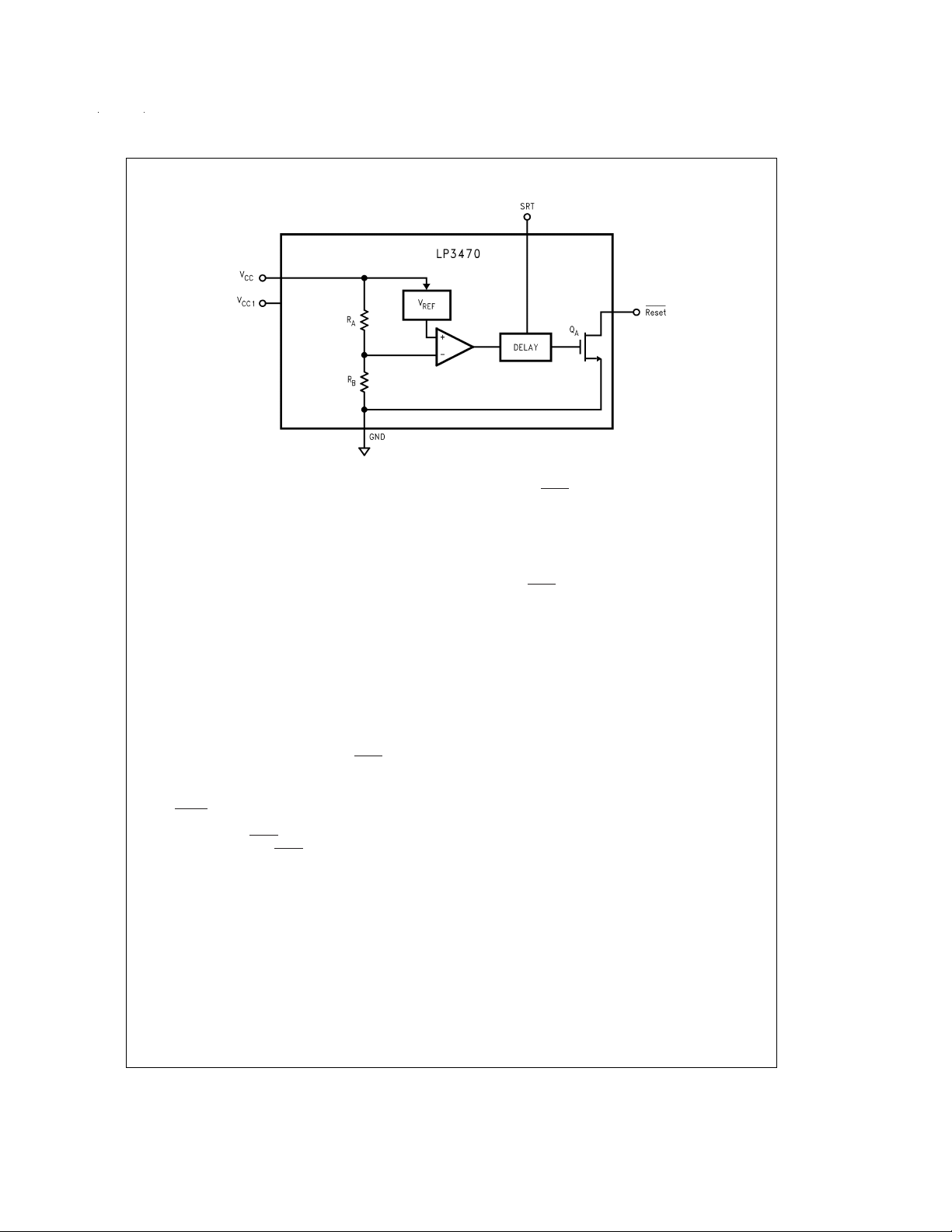
Functional Block Diagram
Application Information
Reset Timeout Period
The Reset Timeout Period (t
external capacitor (C
Ceramic chip capacitor rated at or above 10V is sufficient.
1
The Reset Timeout Period (t
following formula:
t
(ms) = 2000 x C1(µF).
RP
For example a C
no delay due to t
SRT should be left floating.
of 100 nF will achieve a tRPof 200 ms. If
1
is needed in a certain application, the pin
RP
Reset Output
In applications like microprocessor (µP) systems, errors
might occur in system operation during power-up,
power-down, or brownout conditions. It is imperative to
monitor the power supply voltage in order to prevent these
errors from occurring.
The LP3470 asserts a reset signal whenever the V
voltage is below a threshold (V
teed to be a logic low for V
reset threshold, the reset is kept asserted for a time period
(t
) programmed by an external capacitor (C1); after this in-
RP
terval Reset goes to logic high. If a brownout condition occurs (monitored voltage falls below the reset threshold minus
a small hysteresis), Reset goes low. When V
above the reset threshold, Reset remains low for a time period tRPbefore going to logic high.
) is programmable using an
RP
) connected to pin SRT of LP3470. A
) can be calculated using the
RP
supply
CC
CC
returns
) voltage. Reset is guaran-
RTH
>
0.5V.Once VCCexceeds the
CC
DS100016-3
Pull-up Resistor Selection
The LP3470’s Reset output structure is a simple open-drain
N-channel MOSFET switch. Apull-up resistor (R1) should be
connected to V
should be large enough to limit the current through the
R
1
output MOSFET (Q
than 680Ω guarantees this. R
to ensure a logic high while supplying all the leakage current
.
CC
) below 10 mA. A resistor value of more
1
should also be small enough
1
through the Reset pin. A resistor value of less than 68kΩ satisfies this condition. A typical pull-up resistor value of 20 kΩ
is sufficient in most applications.
Negative-Going V
Transients
CC
The LP3470 is relatively immune to short duration
negative-going V
ating Characteristics show the Maximum Transient Duration
transients (glitches). The Typical Oper-
CC
vs. Negative Transient Amplitude (graph titled Transient Rejection), for which reset pulses are not generated. This graph
shows the maximum pulse width a negative-going V
sient may typically have without causing a reset pulse to be
tran-
CC
issued. As the transient amplitude increases (i.e. goes farther below the reset threshold), the maximum allowable
pulse width decreases. A 0.1 µF bypass capacitor mounted
close to V
provides additional transient immunity.
CC
www.national.com5
Page 6
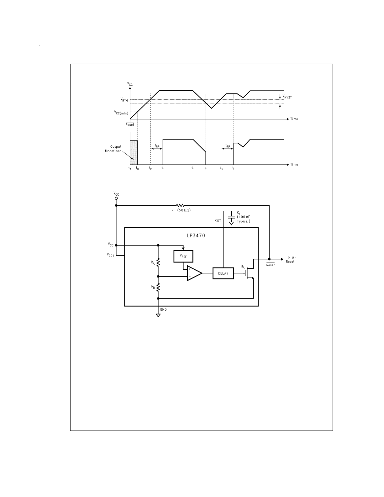
Timing Diagram
Typical Application Circuit
DS100016-4
www.national.com 6
DS100016-5
Page 7
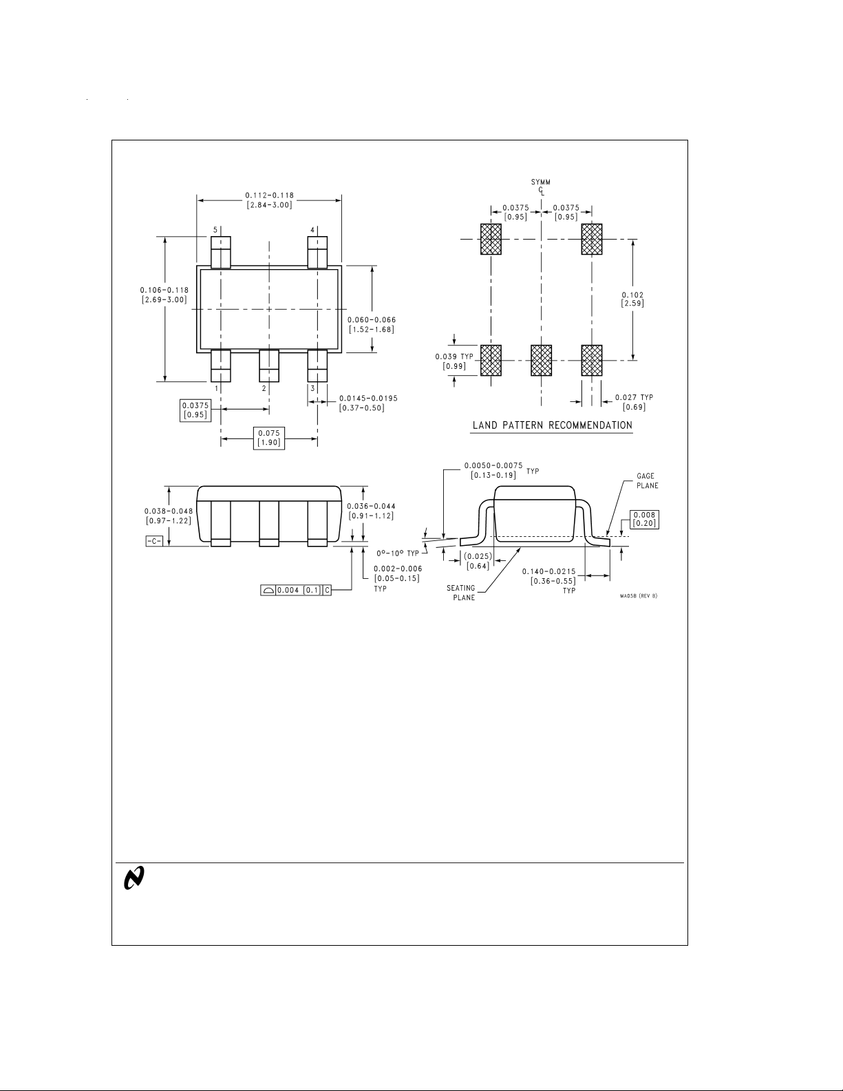
Physical Dimensions inches (millimeters) unless otherwise noted
LP3470 Tiny Power On Reset Circuit
For Ordering Information See
Ordering Information
Table In This Data Sheet
NSPackage Number MA05B
LIFE SUPPORT POLICY
NATIONAL’S PRODUCTS ARE NOT AUTHORIZED FOR USE AS CRITICAL COMPONENTS IN LIFE SUPPORT
DEVICES OR SYSTEMS WITHOUT THE EXPRESS WRITTEN APPROVAL OF THE PRESIDENT AND GENERAL
COUNSEL OF NATIONAL SEMICONDUCTOR CORPORATION. As used herein:
5-Lead Small Outline Package (M5)
1. Life support devices or systems are devices or
systems which, (a) are intended for surgical implant
into the body, or (b) support or sustain life, and
whose failure to perform when properly used in
accordance with instructions for use provided in the
2. A critical component is any component of a life
support device or system whose failure to perform
can be reasonably expected to cause the failure of
the life support device or system, or to affect its
safety or effectiveness.
labeling, can be reasonably expected to result in a
significant injury to the user.
National Semiconductor
Corporation
Americas
Tel: 1-800-272-9959
Fax: 1-800-737-7018
Email: [email protected]
www.national.com
National does not assume any responsibility for use of any circuitry described, no circuit patent licenses are implied and National reserves the right at any time without notice to change said circuitry and specifications.
National Semiconductor
Europe
Fax: +49 (0) 1 80-530 85 86
Email: [email protected]
Deutsch Tel: +49 (0) 1 80-530 85 85
English Tel: +49 (0) 1 80-532 78 32
Français Tel: +49 (0) 1 80-532 93 58
Italiano Tel: +49 (0) 1 80-534 16 80
National Semiconductor
Asia Pacific Customer
Response Group
Tel: 65-2544466
Fax: 65-2504466
Email: [email protected]
National Semiconductor
Japan Ltd.
Tel: 81-3-5639-7560
Fax: 81-3-5639-7507
 Loading...