

Page 1
TL/H/5711
LP311 Voltage Comparator
February 1995
LP311 Voltage Comparator
General Description
The LP311 is a low power version of the industry-standard
LM311. It takes advantage of stable high-value ion-implanted resistors to perform the same function as an LM311, with
a 30:1 reduction in power drain, but only a 6:1 slowdown of
response time. Thus the LP311 is well suited for batterypowered applications, and all other applications where fast
response is not needed. It operates over a wide range of
supply voltages from 36V down to a single 3V supply, with
less than 200 mA drain, but it is still capable of driving a 25
mA load. The LP311 is quite easy to apply without any oscillation, if ordinary precautions are taken to minimize stray
coupling from the output to either input or to the balance
pins (as described in the LM311 datasheet Application
Hints).
Features
Y
Low power drain, 900 mW on 5V supply
Y
Operates fromg15V or a single supply as low as 3V
Y
Output can drive 25 mA
Y
Emitter output can swing below negative supply
Y
Response time: 1.2 ms
Y
Same pin-out as LM311
Y
Low input currents: 2 nA of offset, 15 nA of bias
Y
Large common-mode input range:b14.6V to 13.6V
with
g
15V supply
Applications
Y
Level-detector for battery-powered instruments
Y
Low-power lamp or relay driver
Y
Low-power zero-crossing detector
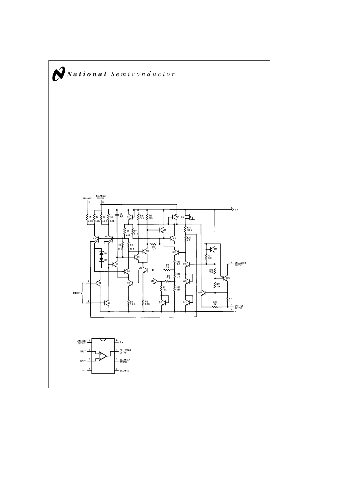
Schematic Diagram
TL/H/5711– 7
Connection Diagram
Dual-In-Line Package
TL/H/5711– 4
Top View
Order Number LP311M or LP311N
See NS Package Numbers M08A or N08E
C
1995 National Semiconductor Corporation RRD-B30M115/Printed in U. S. A.
Page 2
Absolute Maximum Ratings
If Military/Aerospace specified devices are required,
please contact the National Semiconductor Sales
Office/Distributors for availability and specifications.
Total Supply Voltage (V
8–4
) 36V
Collector Output to Negative Supply Voltage (V
7–4
) 40V
Collector Output to Emitter Output 40V
Emitter Output to Negative Supply Voltage (V
1–4
)g30V
Differential Input Voltage
g
30V
Input Voltage (Note 1)
g
15V
Power Dissipation (Note 2) 500 mW
Output Short Circuit Duration 10 sec
Operating Temperature Range 0
§
Cto70§C
Storage Temperature Range
b
65§Cto150§C
Lead Temperature (Soldering, 10 seconds) 260§C
Electrical Characteristics
These specifications apply for V
S
e
g
15V and 0§CsT
A
s
70§C, unless otherwise specified.
Parameter Conditions Min Typ Max Units
Input Offset Voltage (Notes 3, 4) T
A
e
25§C, R
S
s
100k 2.0 7.5 mV
Input Offset Current (Notes 3, 4) T
A
e
25§C 2.0 25 nA
Input Bias Current (Note 3) T
A
e
25§C 15 100 nA
Voltage Gain T
A
e
25§C, R
L
e
5k 40 200 V/mV
Response Time (Note 5) T
A
e
25§C 1.2 ms
Saturation Voltage (Note 6) V
IN
s
b
10 mV, I
OUT
e
25 mA 0.4 1.5 V
T
Ae25§C
Strobe Current (Note 7) T
A
e
25§C 100 200 300 mA
Output Leakage Current V
IN
t
10 mV, V
OUT
e
35V 0.2 100 nA
T
A
e
25§C
Input Offset Voltage (Notes 3, 4) R
S
s
100k 10 mV
Input Offset Current (Notes 3, 4) 35 nA
Input Bias Current (Note 3) 150 nA
Input Voltage Range V
b
a
0.5
a
13.7,b14.7 V
a
b
1.5 V
Saturation Voltage (Note 6) V
a
t
4.5V, V
b
e
0V 0.1 0.4 V
V
IN
s
b
10 mV, I
SINK
s
1.6 mA
Positive Supply Current T
A
e
25§C, Output on 150 300 mA
Negative Supply Current T
A
e
25§C 80 180 mA
Minimum Operating Voltage T
A
e
25§C 3.0 3.5 V
Note 1: This rating applies forg15V supplies. The positive input voltage limit is 30V above the negative supply. The negative input voltage limit is equal to the
negative supply voltage or 30V below the positive supply, whichever is less.
Note 2: The maximum junction temperature of the LP311 is 85
§
C. For operating at elevated temperatures, devices in the dual-in-line package must be derated
based on a thermal resistance of 160
§
C/W, junction to ambient.
Note 3: The offset voltage, offset current and bias current specifications apply for any supply voltage from a single 4V supply up to
g
15V supplies.
Note 4: The offset voltages and offset currents given are the maximum values required to drive the output within a volt of either supply with 1 mA load. Thus, these
parameters define an error band and take into account the worst-case effects of voltage gain and input impedance.
Note 5: The response time specified is for a 100 mV input step with 5 mV overdrive.
Note 6: Saturation voltage specification applies to collector-emitter voltage (V7-1) for V
COLLECTOR
s
(V
a
b
3V).
Note 7: This specification gives the range of current which must be drawn from the strobe pin to ensure the output is properly disabled. Do not short the strobe pin
to ground. It should be current driven, 100 mAto300mA.
2
Page 3

Typical Performance Characteristics
Input Characteristics Input Bias Current Input Offset Current
Common Mode Limits Transfer Function
Output Saturation Voltage
(Collector Output)
Response Time for Various
Input Overdrives
Response Time for Various
Input Overdrives
Output Saturation Voltage
(Emitter Output)
Response Time for Various
Input Overdrives
Response Time for Various
Input Overdrives
Output Limiting
Characteristics
TL/H/5711– 5
3
Page 4

Typical Performance Characteristics (Continued)
Supply Current Supply Current Leakage Currents
TL/H/5711– 6
Applications Information
For applications information and typical applications, refer to the LM311 datasheet.
Auxiliary Circuits
Strobing
TL/H/5711– 1
Note: Do not ground strobe pin.
Offset Balancing
TL/H/5711– 2
Test Circuits
Test Circuit 1 (Collector Output)
TL/H/5711– 8
Test Circuit 2 (Emitter Output)
TL/H/5711– 9
Test Circuit 3 (Collector Output)
TL/H/5711– 10
Test Circuit 4 (Emitter Output)
TL/H/5711– 11
4
Page 5

Physical Dimensions inches (millimeters)
Order Number LP311M
NS Package Number M08A
5
Page 6

LP311 Voltage Comparator
Physical Dimensions inches (millimeters) (Continued)
Molded Dual-In-Line Package (N)
Order Number LP311N
NS Package Number N08E
LIFE SUPPORT POLICY
NATIONAL’S PRODUCTS ARE NOT AUTHORIZED FOR USE AS CRITICAL COMPONENTS IN LIFE SUPPORT
DEVICES OR SYSTEMS WITHOUT THE EXPRESS WRITTEN APPROVAL OF THE PRESIDENT OF NATIONAL
SEMICONDUCTOR CORPORATION. As used herein:
1. Life support devices or systems are devices or 2. A critical component is any component of a life
systems which, (a) are intended for surgical implant support device or system whose failure to perform can
into the body, or (b) support or sustain life, and whose be reasonably expected to cause the failure of the life
failure to perform, when properly used in accordance support device or system, or to affect its safety or
with instructions for use provided in the labeling, can effectiveness.
be reasonably expected to result in a significant injury
to the user.
National Semiconductor National Semiconductor National Semiconductor National Semiconductor
Corporation Europe Hong Kong Ltd. Japan Ltd.
1111 West Bardin Road Fax: (
a
49) 0-180-530 85 86 13th Floor, Straight Block, Tel: 81-043-299-2309
Arlington, TX 76017 Email: cnjwge@tevm2.nsc.com Ocean Centre, 5 Canton Rd. Fax: 81-043-299-2408
Tel: 1(800) 272-9959 Deutsch Tel: (
a
49) 0-180-530 85 85 Tsimshatsui, Kowloon
Fax: 1(800) 737-7018 English Tel: (
a
49) 0-180-532 78 32 Hong Kong
Fran3ais Tel: (
a
49) 0-180-532 93 58 Tel: (852) 2737-1600
Italiano Tel: (
a
49) 0-180-534 16 80 Fax: (852) 2736-9960
National does not assume any responsibility for use of any circuitry described, no circuit patent licenses are implied and National reserves the right at any time without notice to change said circuitry and specifications.
 Loading...