

Page 1
LP2995
DDR Termination Regulator
LP2995 DDR Termination Regulator
July 2003
General Description
The LP2995 linear regulator is designed to meet the JEDEC
SSTL-2 and SSTL-3 specifications for termination of DDRSDRAM. The device contains a high-speed operational amplifier to provide excellent response to load transients. The
output stage prevents shoot through while delivering 1.5A
continuous current and transient peaks up to 3A in the
application as required for DDR-SDRAM termination. The
LP2995 also incorporates a V
load regulation and a V
chipset and DDR DIMMS.
Patents Pending
REF
pin to provide superior
SENSE
output as a reference for the
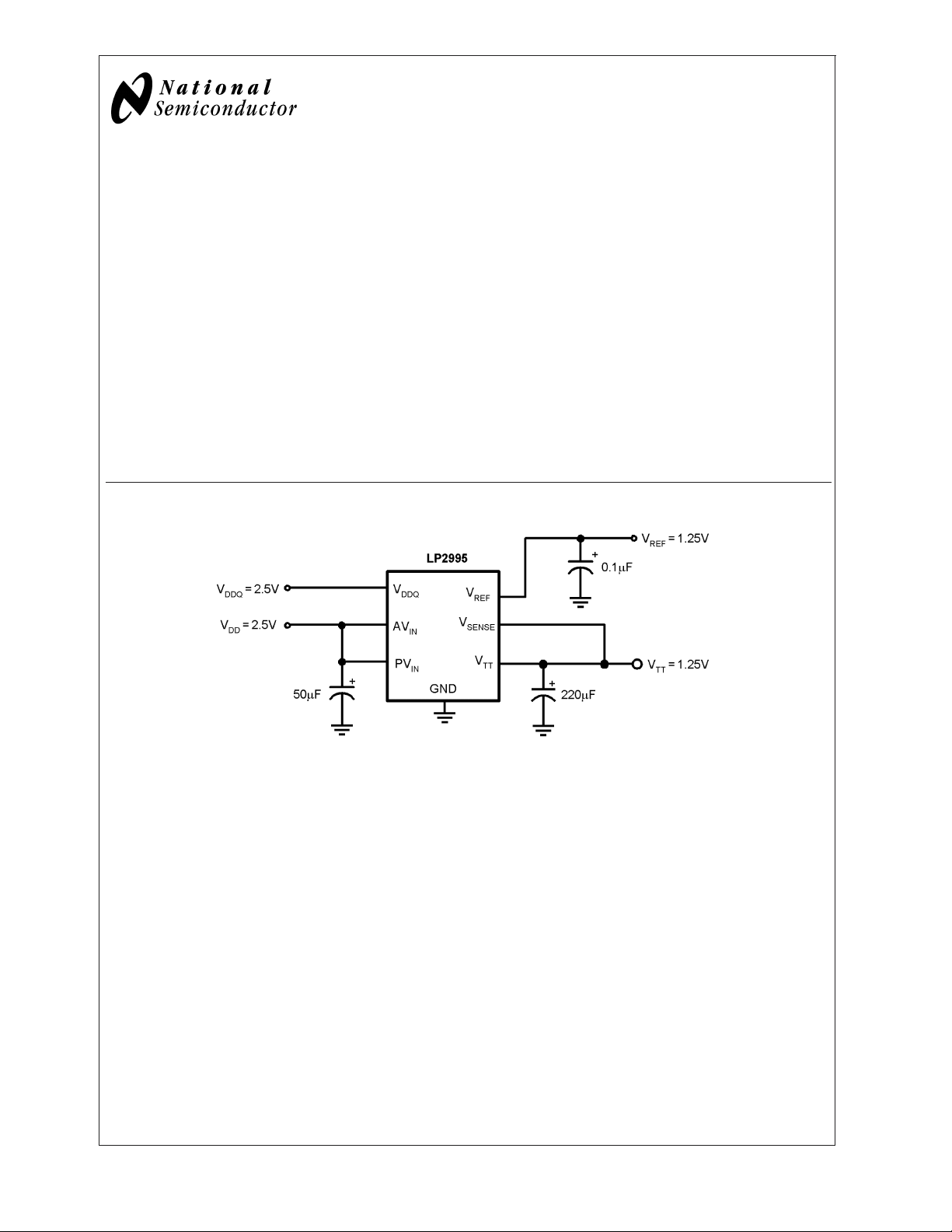
Typical Application Circuit
Features
n Low output voltage offset
n Works with +5v, +3.3v and 2.5v rails
n Source and sink current
n Low external component count
n No external resistors required
n Linear topology
n Available in SO-8, PSOP-8 or LLP-16 packages
n Low cost and easy to use
Applications
n DDR Termination Voltage
n SSTL-2
n SSTL-3
20039302
© 2003 National Semiconductor Corporation DS200393 www.national.com
Page 2
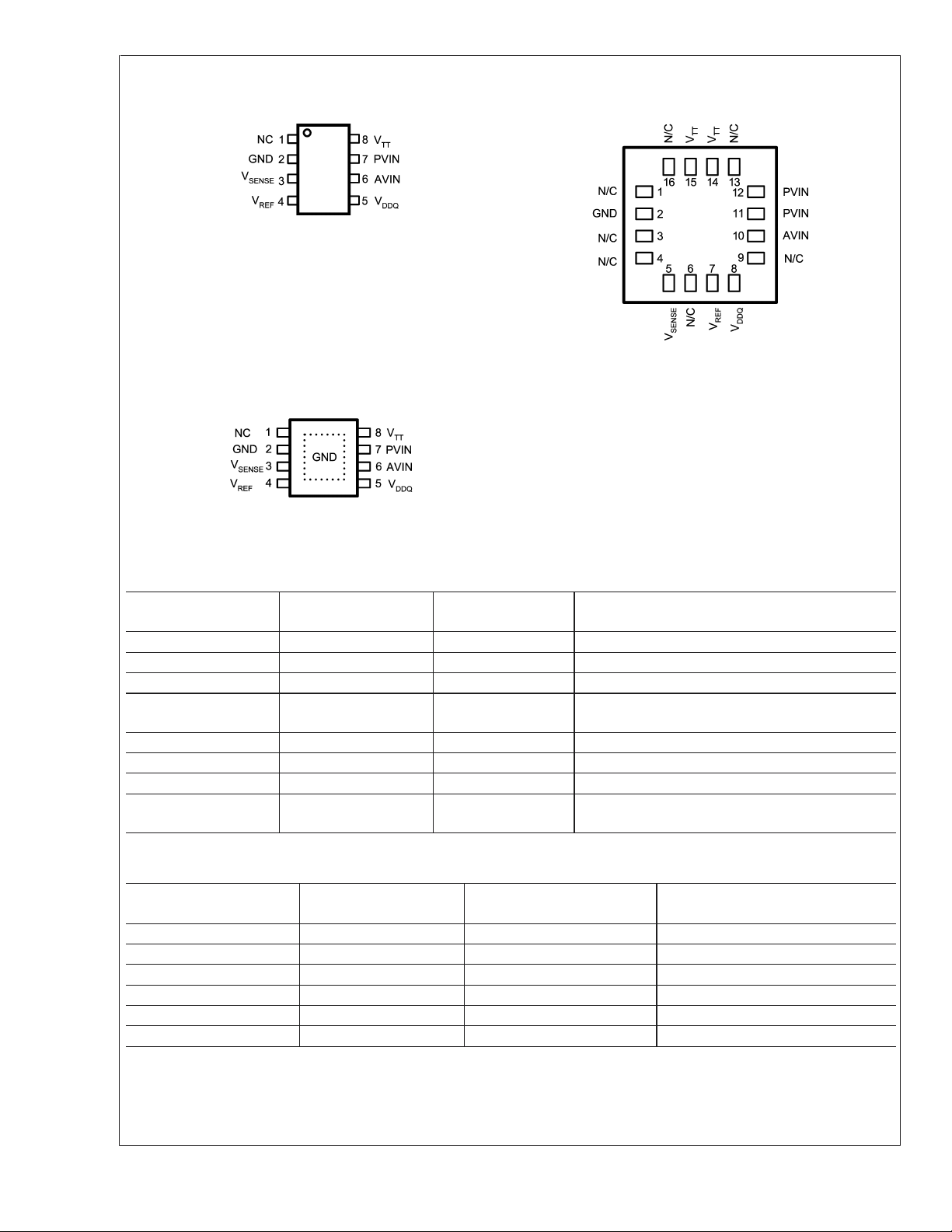
Connection Diagrams
LP2995
SO-8 (M08A) Package LQA- 16 Package
PSOP-8 (MRA08A) Package
Pin Description
SO-8 Pin or
PSOP-8 Pin
1 1,3,4,6,9, 13,16 NC No internal connection. Can be used for vias.
2 2 GND Ground.
3 5 VSENSE Feedback pin for regulating VTT.
4 7 VREF Buffered internal reference voltage of
5 8 VDDQ Input for internal reference equal to VDDQ/2.
6 10 AVIN Analog input pin.
7 11, 12 PVIN Power input pin.
8 14, 15 VTT Output voltage for connection to termination
Top View
20039320
20039304
Top View
20039350
Top View
LLP Pin Name Function
VDDQ/2.
resistors.
Ordering Information
Order Number Package Type
LP2995M SO-8 M08A 95 Units per Rail
LP2995MX SO-8 M08A 2500 Units Tape and Reel
LP2995MR PSOP-8 MRA08A 95 Units per Rail
LP2995MRX PSOP-8 MRA08A 2500 Units Tape and Reel
LP2995LQ LLP-16 LQA16A 1000 Units Tape and Reel
LP2995LQX LLP-16 LQA16A 4500 Units Tape and Reel
www.national.com 2
NSC Package
Drawing
Supplied As
Page 3
LP2995
Absolute Maximum Ratings (Note 1)
If Military/Aerospace specified devices are required,
Lead Temperature (Soldering, 10 sec) 260˚C
ESD Rating (Note 7) 1kV
please contact the National Semiconductor Sales Office/
Distributors for availability and specifications.
Operating Range
PVIN, AVIN, VDDQ to GND −0.3V to +6V
Storage Temp. Range −65˚C to +150˚C
Junction Temperature 150˚C
SO-8 Thermal Resistance (θ
LLP-16 Thermal Resistance (θ
) 151˚C/W
JA
) 51˚C/W
JA
Electrical Characteristics Specifications with standard typeface are for T
type apply over the full Operating Temperature Range (T
AVIN = PVIN = 2.5V, VDDQ = 2.5V (Note 6).
Symbol Parameter Conditions Min Typ Max Units
V
REF
VOS
VTT
V
Voltage I
REF
VTTOutput Voltage Offset I
REF_OUT
OUT
(Note 2)
∆V
Z
Z
I
q
TT/VTT
VREF
VDDQ
Load Regulation
(Note 3)
V
Output Impedance I
REF
VDDQ Input Impedance 100 kΩ
Quiescent Current I
I
I
OUT
OUT
REF
OUT
(Note 4)
Note 1: Absolute maximum ratings indicate limits beyond which damage to the device may occur. Operating range indicates conditions for which the device is
intended to be functional, but does not guarantee specific performance limits. For guaranteed specifications and test conditions see Electrical Characteristics. The
guaranteed specifications apply only for the test conditions listed. Some performance characteristics may degrade when the device is not operated under the listed
test conditions.
Note 2: V
Note 3: Load regulation is tested by using a 10ms current pulse and measuring V
Note 4: Quiescent current defined as the current flow into AVIN.
Note 5: At elevated temperatures, devices must be derated based on thermal resistance. The device in the SO-8 package must be derated at θ
junction to ambient with no heat sink. The device in the LLP-16 must be derated at θ
Note 6: Limits are 100% production tested at 25˚C. Limits over the operating temperature range are guaranteed through correlation using Statistical Quality Control
(SQC) methods. The limits are used to calculate National’s Average Outgoing Quality Level (AOQL).
Note 7: The human body model is a 100pF capacitor discharged through a 1.5kΩ resistor into each pin.
offset is the voltage measurement defined as V
TT
subtracted from V
TT
J
= 0mA 1.21 1.235 1.26 V
=0A
= 0 to 1.5A 0.5 %
= 0 to −1.5A −0.5
= −5µA to +5µA 5 kΩ
=0A
Junction Temp. Range (Note 5) 0˚C to +125˚C
AVIN to GND 2.2V to 5.5V
PVIN to GND 2.2V to AVIN
= 25˚C and limits in boldface
J
= 0˚C to +125˚C). Unless otherwise specified,
−15
01520mV
−20
250 400 µA
.
REF
.
TT
= 51˚ C/W junction to ambient.
JA
= 151˚ C/W
JA
www.national.com3
Page 4
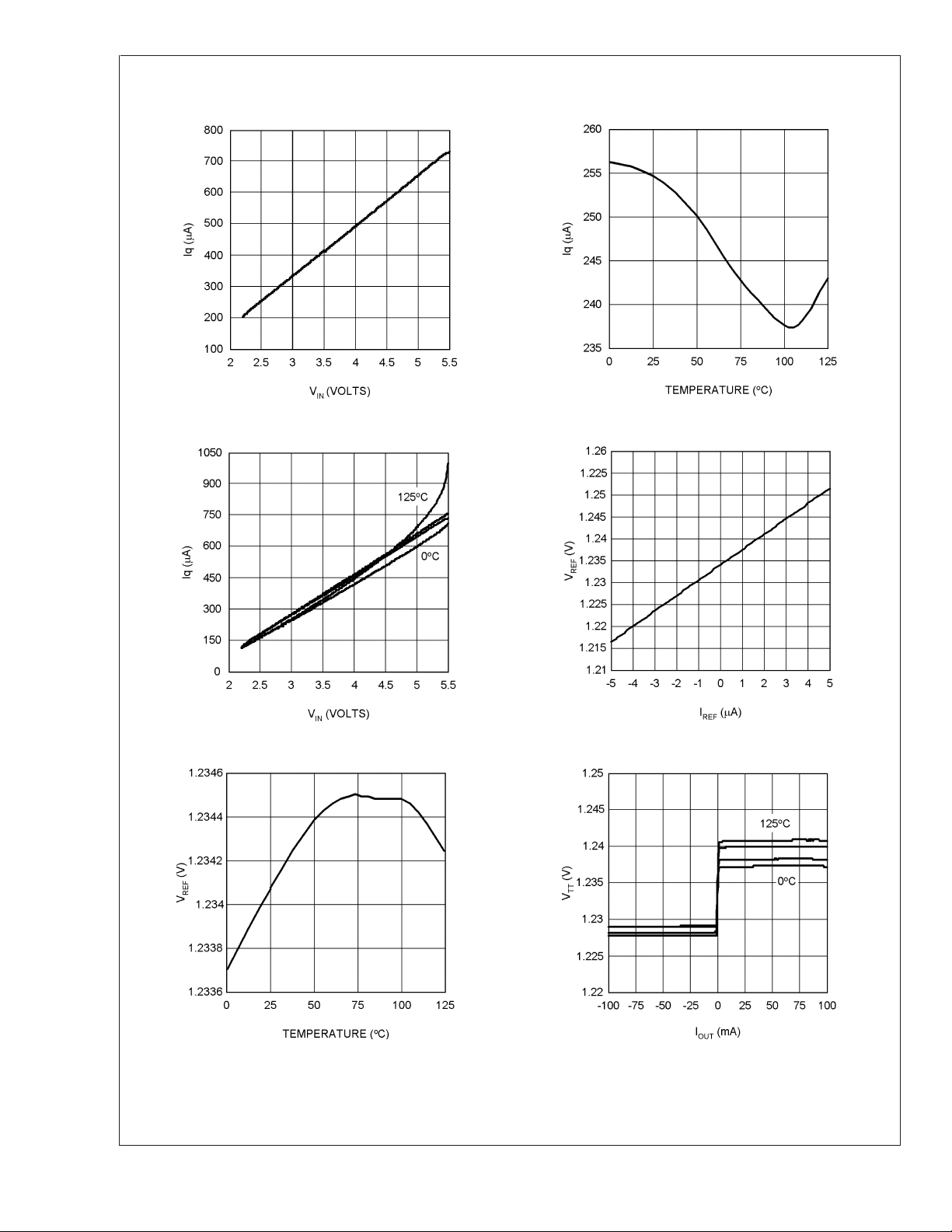
Typical Performance Characteristics
LP2995
Iq vs VIN(0, 25, 85, and 125˚C) V
Iq vs VIN(25˚C) Iq vs Temperature ( VIN= 2.5V)
20039309 20039310
vs I
REF
REF
20039311 20039312
V
vs Temperature (No Load) VTTvs I
REF
20039313 20039314
www.national.com 4
(0, 25, 85, and 125˚C)
OUT
Page 5

Typical Performance Characteristics (Continued)
LP2995
V
vs I
TT
OUT
20039315
Maximum Output Current (Sinking) vs V
(VDDQ = 2.5)
Maximum Output Current (Sourcing) vs V
IN
(VDDQ = 2.5)
20039316
IN
20039317
www.national.com5
Page 6

Block Diagram
LP2995
20039301
Description
The LP2995 is a linear bus termination regulator designed to
meet the JEDEC requirements of SSTL-2 and SSTL-3. The
LP2995 is capable of sinking and sourcing current at the
output V
buffered reference voltage that also tracks VDDQ/2is
generated on the V
the DDR-SDRAM and Northbridge Chipset. V
to track the V
entire current range while preventing shoot through on the
output stage.
Series Stub Termination Logic (SSTL) was created to improve signal integrity of the data transmission across the
memory bus. This termination scheme is essential to prevent
data error from signal reflections while transmitting at high
frequencies encountered with DDR RAM. The most common
form of termination is Class II single parallel termination. This
involves using one Rs series resistor from the chipset to the
memory and one Rt termination resistor. This implementation can be seen below in Figure 1.
, regulating the voltage to equal VDDQ / 2. A
TT
pin for providing a global reference to
REF
voltage with a tight tolerance over the
REF
is designed
TT
Typical values for R
and RTare 25 Ohms although these
S
can be changed to scale the current requirements from the
LP2995. For determination of the current requirements of
DDR-SDRAM termination please refer to the accompanying
application notes.
20039308
FIGURE 1.
www.national.com 6
Page 7

Pin Descriptions
AVIN AND PVIN
AVIN and PVIN are the input supply pins for the LP2995.
AVIN is used to supply all the internal control circuitry for the
two op-amps and the output stage of V
exclusively to provide the rail voltage for the output stage on
the power operational amplifier used to create V
SSTL-2 applications AVIN and PVIN pins should be connected directly and tied to the 2.5V rail for optimal performance. This eliminates the need for bypassing the two supply pins separately.
VDDQ
VDDQ is the input that is used to create the internal reference voltage for regulating V
TT
and V
generated by two internal 50kΩ resistors. This guarantees
that V
TT
and V
will track VDDQ / 2 precisely. The optimal
REF
implementation of VDDQ is as a remote sense for the reference input. This can be achieved by connecting VDDQ
directly to the 2.5V rail at the DIMM. This ensures that the
reference voltage tracks the DDR memory rails precisely
without a large voltage drop from the power lines. For
SSTL-2 applications VDDQ will be a 2.5V signal, which will
create a 1.25V reference voltage on V
termination voltage at V
. For SSTL-3 applications it may
TT
be desirable to have a different scaling factor for creating the
internal reference voltage besides 0.5. For instance a typical
value that is commonly used is to have the reference voltage
*
equal VDDQ
0.45. This can be achieved by placing a resistor in series with the VDDQ pin to effectively change the
resistor divider.
V
SENSE
The purpose of the sense pin is to provide improved remote
load regulation. In most motherboard applications the termination resistors will connect to V
TT
output voltage was regulated only at the output of the
LP2995, then the long trace will cause a significant IR drop,
resulting in a termination voltage lower at one end of the bus
than the other. The V
pin can be used to improve this
SENSE
performance, by connecting it to the middle of the bus. This
will provide a better distribution across the entire termination
bus.
Note: If remote load regulation is not used, then the V
connected to V
V
REF
V
provides the buffered output of the internal reference
REF
.
TT
voltage VDDQ / 2. This output should be used to provide the
reference voltage for the Northbridge chipset and memory.
Since these inputs are typically an extremely high impedance, there should be little current drawn from V
improved performance, an output bypass capacitor can be
used, located close to the pin, to help with noise. A ceramic
capacitor in the range of 0.1 µF to 0.01 µF is recommended.
V
TT
VTTis the regulated output that is used to terminate the bus
resistors. It is capable of sinking and sourcing current while
regulating the output precisely to VDDQ / 2. The LP2995 is
designed to handle peak transient currents of up to
a fast transient response. The maximum continuous current
is a function of V
and can be viewed in the TYPICAL
IN
PERFORMANCE CHARACTERISTICS section. If a transient is expected to last above the maximum continuous
. PVIN is used
REF
. For
TT
. This voltage is
REF
and a 1.25V
REF
in a long plane. If the
pin must still be
SENSE
. For
REF
±
3A with
current rating for a significant amount of time then the output
capacitor should be sized large enough to prevent an excessive voltage drop. Despite the fact that the LP2995 is designed to handle large transient output currents it is not
capable of handling these for long durations, under all conditions. The reason for this is the standard packages are not
able to thermally dissipate the heat as a result of the internal
power loss. If large currents are required for longer durations, then care should be taken to ensure that the maximum
junction temperature is not exceeded. Proper thermal derating should always be used (please refer to the Thermal
Dissipation section).
Component Selection
INPUT CAPACITOR
The LP2995 does not require a capacitor for input stability,
but it is recommended for improved performance during
large load transients to prevent the input rail from dropping.
The input capacitor should be located as close as possible to
the PVIN pin. Several recommendations exist dependent on
the application required. A typical value recommended for AL
electrolytic capacitors is 50 µF. Ceramic capacitors can also
be used, a value in the range of 10 µF with X5R or better
would be an ideal choice. The input capacitance can be
reduced if the LP2995 is placed close to the bulk capacitance from the output of the 2.5V DC-DC converter.
OUTPUT CAPACITOr
The LP2995 has been designed to be insensitive of output
capacitor size or ESR (Equivalent Series Resistance). This
allows the flexibility to use any capacitor desired. The choice
for output capacitor will be determined solely on the application and the requirements for load transient response of V
As a general recommendation the output capacitor should
be sized above 100 µF with a low ESR for SSTL applications
with DDR-SDRAM. The value of ESR should be determined
by the maximum current spikes expected and the extent at
which the output voltage is allowed to droop. Several capacitor options are available on the market and a few of these
are highlighted below:
AL - It should be noted that many aluminum electrolytics only
specify impedance at a frequency of 120 Hz, which indicates
they have poor high frequency performance. Only aluminum
electrolytics that have an impedance specified at a higher
frequency (between 20 kHz and 100 kHz) should be used for
the LP2995. To improve the ESR several AL electrolytics can
be combined in parallel for an overall reduction. An important
note to be aware of is the extent at which the ESR will
change over temperature. Aluminum electrolytic capacitors
can have their ESR rapidly increase at cold temperatures.
Ceramic - Ceramic capacitors typically have a low capacitance, in the range of 10 to 100 µF range, but they have
excellent AC performance for bypassing noise because of
very low ESR (typically less than 10 mΩ). However, some
dielectric types do not have good capacitance characteristics as a function of voltage and temperature. Because of the
typically low value of capacitance it is recommended to use
ceramic capacitors in parallel with another capacitor such as
an aluminum electrolytic. A dielectric of X5R or better is
recommended for all ceramic capacitors.
Hybrid - Several hybrid capacitors such as OS-CON and SP
are available from several manufacturers. These offer a
large capacitance while maintaining a low ESR. These are
TT
LP2995
.
www.national.com7
Page 8

Component Selection (Continued)
LP2995
the best solution when size and performance are critical,
although their cost is typically higher than any other capacitor.
Capacitor recommendations for different application circuits
can be seen in the accompanying application notes with
supporting evaluation boards.
Thermal Dissipation
Since the LP2995 is a linear regulator any current flow from
will result in internal power dissipation generating heat.
V
TT
To prevent damaging the part from exceeding the maximum
allowable junction temperature, care should be taken to
derate the part dependent on the maximum expected ambient temperature and power dissipation. The maximum allowable internal temperature rise (T
given the maximum ambient temperature (T
application and the maximum allowable junction temperature
).
(T
Jmax
T
Rmax=TJmax−TAmax
From this equation, the maximum power dissipation (P
of the part can be calculated:
P
Dmax=TRmax
The θJAof the LP2995 will be dependent on several variables: the package used; the thickness of copper; the number of vias and the airflow. For instance, the θ
is 163˚C/W with the package mounted to a standard 8x4
2-layer board with 1oz. copper, no airflow, and 0.5W dissipation at room temperature. This value can be reduced to
151.2˚C/W by changing to a 3x4 board with 2 oz. copper that
is the JEDEC standard. Figure 2 shows how the θ
with airflow for the two boards mentioned.
) can be calculated
Rmax
/ θ
JA
)ofthe
Amax
of the SO-8
JA
JA
Dmax
varies
the DAP the θ
can be lowered significantly. Figure 3 shows
JA
the LLP thermal data when placed on a 4-layer JEDEC
board with copper thickness of 0.5/1/1/0.5 oz. The number of
vias, with a pitch of 1.27 mm, has been increased to the
maximum of 4 where a θ
of 50.41˚C/W can be obtained.
JA
Via wall thickness for this calculation is 0.036 mm for 1oz.
Copper.
)
LLP-16 θJAvs#of Vias (4 Layer JEDEC Board))
20039322
FIGURE 3.
Additional improvements in lowering the θ
can also be
JA
achieved with a constant airflow across the package. Maintaining the same conditions as above and utilizing the 2x2
via array, Figure 4 shows how the θ
varies with airflow.
JA
θJAvs Airflow (SO-8)
20039321
FIGURE 2.
Layout is also extremely critical to maximize the output
current with the LLP package. By simply placing vias under
www.national.com 8
θJAvs Airflow Speed (JEDEC Board with 4 Vias)
20039323
FIGURE 4.
Page 9

Typical Application Circuits
The typical application circuit used for SSTL-2 termination
schemes with DDR-SDRAM can be seen in Figure 5.
LP2995
SSTL-2 Implementation
For SSTL-3 and other applications it may be desirable to
*
change internal reference voltage scaling from VDDQ
0.5.
An external resistor in series with the VDDQ pin can be used
to lower the reference voltage. Internally two 50 kΩ resistors
SSTL-3 Implementation
FIGURE 5.
FIGURE 6.
20039306
set the output V
to be equal to VDDQ*0.5. The addition
TT
of a 11.1 kΩ external resistor will change the internal refer-
*
ence voltage causing the two outputs to track VDDQ
0.45.
An implementation of this circuit can be seen in Figure 6.
20039307
Another application that is sometimes required is to increase
output voltage from the scaling factor of VDDQ*0.5.
the V
TT
This can be accomplished independently of V
REF
by using a
FIGURE 7.
resistor divider network between V
TT,VSENSE
and Ground.
An example of this circuit can be seen in Figure 7.
20039303
www.national.com9
Page 10

PCB Layout Considerations
1. AVIN and PVIN should be tied together for optimal per-
LP2995
formance. A local bypass capacitor should be placed as
close as possible to the PVIN pin.
2. GND should be connected to a ground plane with multiple vias for improved thermal performance.
3. V
should be connected to the VTTtermination bus
SENSE
at the point where regulation is required. For motherboard applications an ideal location would be at the
center of the termination bus.
4. VDDQ can be connected remotely to the VDDQ rail
input at either the DIMM or the Chipset. This provides
the most accurate point for creating the reference voltage.
5. V
should be bypassed with a 0.01 µF or 0.1 µF
REF
ceramic capacitor for improved performance. This capacitor should be located as close as possible to the
pin.
V
REF
www.national.com 10
Page 11

Physical Dimensions inches (millimeters)
unless otherwise noted
LP2995
8-Lead Small Outline Package (M8)
NS Package Number M08A
www.national.com11
Page 12

Physical Dimensions inches (millimeters) unless otherwise noted (Continued)
LP2995
16-Lead LLP Package (LD)
NS Package Number LQA16A
8-Lead PSOP Package (PSOP-8)
NS Package Number MRA08A
www.national.com 12
Page 13

Notes
LP2995 DDR Termination Regulator
LIFE SUPPORT POLICY
NATIONAL’S PRODUCTS ARE NOT AUTHORIZED FOR USE AS CRITICAL COMPONENTS IN LIFE SUPPORT
DEVICES OR SYSTEMS WITHOUT THE EXPRESS WRITTEN APPROVAL OF THE PRESIDENT AND GENERAL
COUNSEL OF NATIONAL SEMICONDUCTOR CORPORATION. As used herein:
1. Life support devices or systems are devices or
systems which, (a) are intended for surgical implant
into the body, or (b) support or sustain life, and
whose failure to perform when properly used in
accordance with instructions for use provided in the
2. A critical component is any component of a life
support device or system whose failure to perform
can be reasonably expected to cause the failure of
the life support device or system, or to affect its
safety or effectiveness.
labeling, can be reasonably expected to result in a
significant injury to the user.
National Semiconductor
Americas Customer
Support Center
Email: new.feedback@nsc.com
Tel: 1-800-272-9959
www.national.com
National does not assume any responsibility for use of any circuitry described, no circuit patent licenses are implied and National reserves the right at any time without notice to change said circuitry and specifications.
National Semiconductor
Europe Customer Support Center
Fax: +49 (0) 180-530 85 86
Email: europe.support@nsc.com
Deutsch Tel: +49 (0) 69 9508 6208
English Tel: +44 (0) 870 24 0 2171
Français Tel: +33 (0) 1 41 91 8790
National Semiconductor
Asia Pacific Customer
Support Center
Email: ap.support@nsc.com
National Semiconductor
Japan Customer Support Center
Fax: 81-3-5639-7507
Email: jpn.feedback@nsc.com
Tel: 81-3-5639-7560
 Loading...