

Page 1
LP2994
DDR Termination Regulator
LP2994 DDR Termination Regulator
June 2005
General Description
The LP2994 regulator is designed to provide a linear solution
to meet the JEDEC SSTL-2 and SSTL-3 specifications (Series Stub Termination Logic) for active termination of DDRSDRAM. The device utilizes an internal operational amplifier
to provide linear regulation of V
expensive external components. The output stage prevents
shoot through while delivering 1.5A continuous current and
maintaining excellent load regulation. The LP2994 also incorporates an active low shutdown pin to tri-state the output
during Suspend To Ram (STR) states.
Patents Pending
without the need for
TT
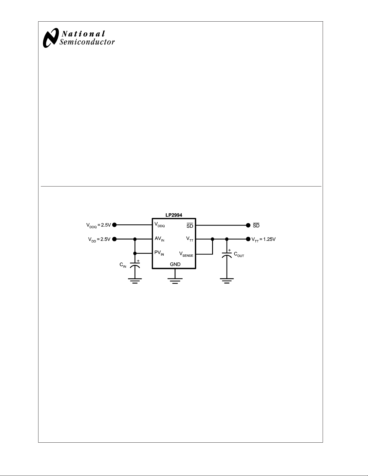
Typical Application Circuit
Features
n Source and sink current
n Low external component count
n Independent analog and power rails
n Linear topology
n Small package SO-8
n Low cost and easy to use
n Shutdown pin
Applications
n SSTL-2
n SSTL-3
n DDR-SDRAM Termination
n DDR-II Termination
20045904
FIGURE 1. SSTL-2 VTTTermination
© 2005 National Semiconductor Corporation DS200459 www.national.com
Page 2
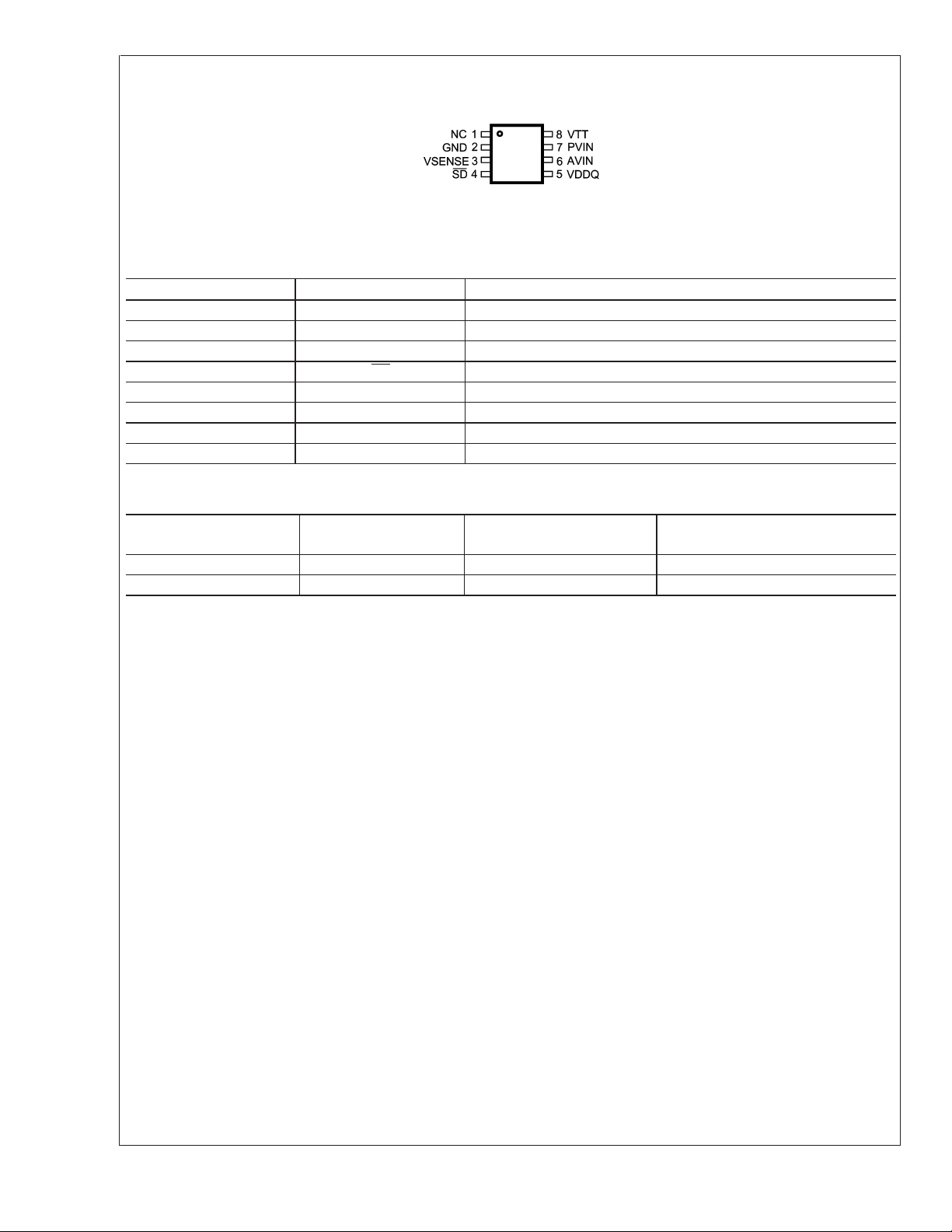
Connection Diagram
LP2994
SO-8 (M08A) Package
Top View
20045902
Pin Descriptions
SO-8 Pin Name Function
1 NC No internal connection
2 GND Ground
3 VSENSE Feedback pin for regulating VTT
4SD
5 VDDQ Input for internal reference equal to VDDQ/2
6 AVIN Analog input pin
7 PVIN Power input pin
8 VTT Output voltage for connection to termination resistors
Active low shutdown pin
Ordering Information
Order Number Package Type
LP2994M SO-8 M08A 95 Units per Rail
LP2994MX SO-8 M08A 2500 Units Tape and Reel
NSC Package
Drawing
Supplied As
www.national.com 2
Page 3
LP2994
Absolute Maximum Ratings (Note 1)
If Military/Aerospace specified devices are required,
please contact the National Semiconductor Sales Office/
Distributors for availability and specifications.
PVIN, AVIN, VTT, VDDQ, SD to GND −0.3V to +6V
Storage Temp. Range −65˚C to +150˚C
Junction Temperature 150˚C
PVIN Supply Voltage -0.3V to (AVIN +
0.3V)
SD Input Voltage -0.3V to (AVIN +
0.3V)
VTT Output Voltage -0.3V to (PVIN +
0.3V)
SO-8 Thermal Resistance (θ
) 151˚C/W
JA
Lead Temperature (Soldering, 10 sec) 260˚C
ESD Rating (Note 2) 2kV
Operating Range
Junction Temp. Range (Note 3) 0˚C to +125˚C
AVIN Supply Voltage 2.2V to 5.5V
Electrical Characteristics Specifications with standard typeface are for T
type apply over the full Operating Temperature Range (T
AVIN = PVIN = 2.5V, VDDQ = 2.5V (Note 4).
Symbol Parameter Conditions Min Typ Max Units
V
TT
VTTOutput Voltage
= 0A (Note 5)
I
OUT
VIN=VDDQ = 2.3V 1.108 1.138 1.168
VIN=VDDQ = 2.7V 1.305 1.334 1.360
I
q
Quiescent Current I
OUT
(Note 6)
Z
I
QSD
VDDQ
VDDQ Input Impedance 86 100 kΩ
Quiescent current in
shutdown
I
SD
V
IH
Shutdown Leakage
Current
Minimum Shutdown High
SD=0V
SD = 2.5V
Level
V
IL
Maximum Shutdown Low
Level
∆V
TT/VTT
Load Regulation
(Note 7)
I
SENSE
Note 1: Absolute maximum ratings indicate limits beyond which damage to the device may occur. Operating range indicates conditions for which the device is
intended to be functional, but does not guarantee specific performance limits. For guaranteed specifications and test conditions see Electrical Characteristics. The
guaranteed specifications apply only for the test conditions listed. Some performance characteristics may degrade when the device is not operated under the listed
test conditions.
Note 2: The human body model is a 100pF capacitor discharged through a 1.5kΩ resistor into each pin.
Note 3: At elevated temperatures, devices must be derated based on thermal resistance. The device in the SO-8 package must be derated at θ
junction to ambient with no heat sink.
Note 4: Limits are 100% production tested at 25˚C. Limits over the operating temperature range are guaranteed through correlation using Statistical Quality Control
(SQC) methods. The limits are used to calculate National’s Average Outgoing Quality Level (AOQL).
Note 5: VIN is defined as the VIN = AVIN = PVIN
Note 6: Quiescent current defined as the current flow into AVIN.
Note 7: Load regulation is tested by using a 10ms current pulse and measuring V
SENSE Input Current 100 pA
I
I
OUT
OUT
= 0˚C to +125˚C). Unless otherwise specified,
J
=0A
1.9 V
= 0 to 1.5A -0.4 %
= 0 to −1.5A +0.4
.
TT
= 25˚C and limits in boldface
J
272 400 µA
21 45 µA
2
5 µA
2
0.8 V
= 151.2˚ C/W
JA
nA
VVIN=VDDQ = 2.5V 1.210 1.236 1.260
www.national.com3
Page 4
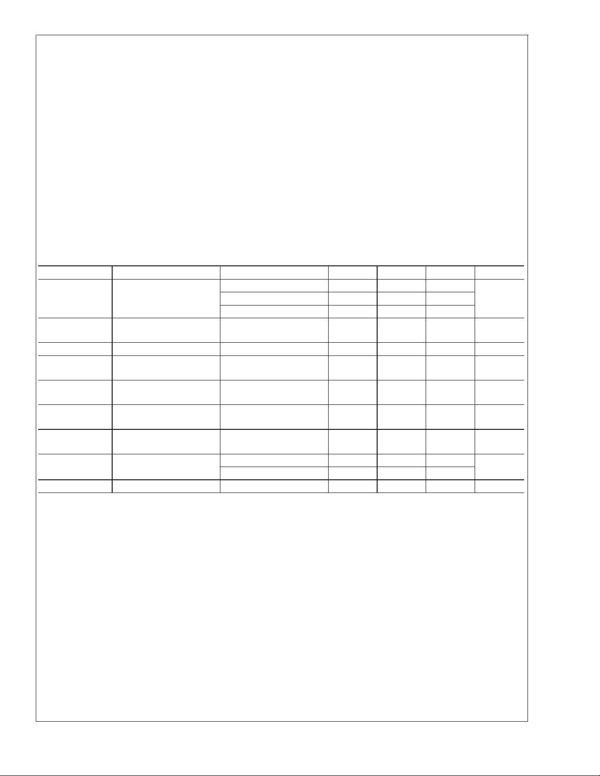
Typical Performance Characteristics
LP2994
Iq vs Temperature ( VIN= 2.5V) ISDvs VIN(25˚C)
Iq vs VIN(25˚C) Iq vs VIN(0, 25, and 125˚C)
20045914 20045915
20045916
ISDvs VIN(0, 25, and 125˚C) ISDvs Temperature ( VIN= 2.5V)
20045918
www.national.com 4
20045917
20045919
Page 5
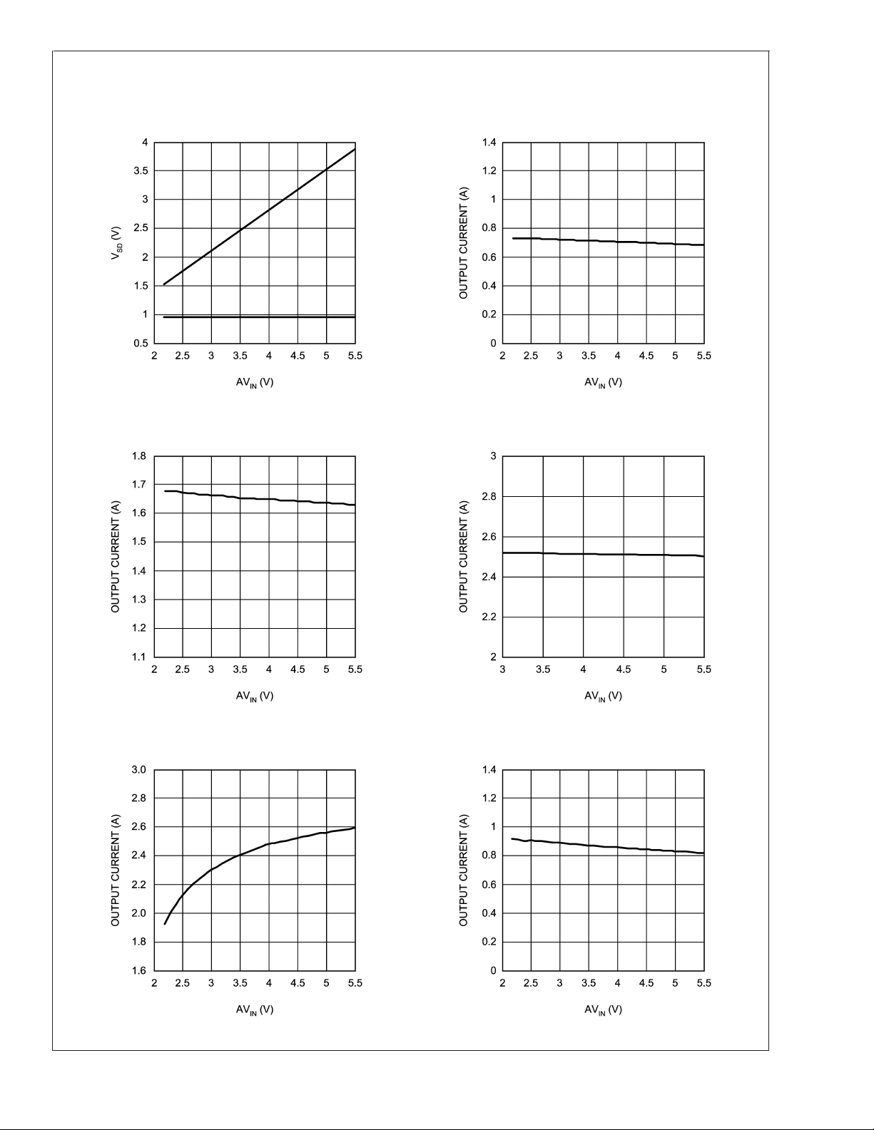
Typical Performance Characteristics (Continued)
LP2994
V
and VIHvs AVIN(25˚C)
IL
Maximum Sourcing Current vs AV
(V
= 2.5V, PVIN= 2.5V)
DDQ
Maximum Sourcing Current vs AV
(V
= 2.5V, PVIN= 1.8V)
DDQ
20045920 20045921
IN
Maximum Sourcing Current vs AV
(V
= 2.5V, PVIN= 3.3V)
DDQ
IN
IN
Maximum Sinking Current vs AV
(V
= 2.5V)
DDQ
20045922 20045923
IN
20045924 20045925
Maximum Sourcing Current vs AV
(V
= 1.8V, PVIN= 1.8V)
DDQ
IN
www.national.com5
Page 6

Typical Performance Characteristics (Continued)
LP2994
Maximum Sinking Current vs AV
(V
= 1.8V)
DDQ
VTTvs I
(0, 25, 85, and 125˚C) VTTvs I
OUT
IN
20045926 20045927
Maximum Sourcing Current vs AV
(V
= 1.8V, PVIN= 3.3V)
DDQ
OUT
IN
20045929 20045930
www.national.com 6
Page 7

Block Diagram
LP2994
20045903
Description
The LP2994 is a linear bus termination regulator designed to
meet the JEDEC requirements of SSTL-2 and SSTL-3. The
output, V
regulating the output voltage equal to V
stage has been designed to maintain excellent load regulation while preventing shoot through. The LP2994 also incorporates two distinct power rails which separates the analog
circuitry from the power output stage. This allows a split rail
approach to be utilized to decrease internal power dissipation. It also permits the LP2994 to provide a termination
solution for the next generation of DDR-SDRAM memory
(DDRII).
Series Stub Termination Logic (SSTL) was created to improve signal integrity of the data transmission across the
memory bus. This termination scheme is essential to prevent
data error from signal reflections while transmitting at high
frequencies encountered with DDR-SDRAM. The most common form of termination is Class II single parallel termination. This involves one R
is capable of sinking and sourcing current while
TT
series resistor from the chipset to
S
/ 2. The output
DDQ
the memory and one R
and RTare 25 Ohms, although these can be changed
for R
S
termination resistor. Typical values
T
to scale the current requirements from the LP2994. This
implementation can be seen below in Figure 2.
20045931
FIGURE 2. SSTL Termination Scheme
www.national.com7
Page 8

Pin Descriptions
LP2994
AVIN and PVIN
AVIN and PVIN are the input supply pins for the LP2994.
AVIN is used to supply all the internal control circuitry. PVIN,
however, is used exclusively to provide the rail voltage for
the output stage used to create V
capability to work off separate supplies depending on the
application. Higher voltages on PVIN will increase the maximum continuous output current because of output RDSON
limitations at voltages close to V
values of PVIN is that the internal power loss will also
increase, thermally limiting the design. For SSTL-2 applications, a good compromise would be to connect the AVIN and
PVIN directly together at 2.5V. This eliminates the need for
bypassing the two supply pins separately. The only limitation
on input voltage selection is that PVIN must be equal to or
lower than AVIN.
V
DDQ
V
is the input used to create the internal reference
DDQ
voltage for regulating V
. The reference voltage is gener-
TT
ated from a resistor divider of two internal 50kΩ resistors.
This guarantees that V
optimal implementation of V
will track V
TT
DDQ
can be achieved by connecting V
at the DIMM instead of AVIN and PVIN. This ensures that the
reference voltage tracks the DDR memory rails precisely
without a large voltage drop from the power lines. For
SSTL-2 applications V
will be a 2.5V signal, which will
DDQ
create a 1.25V termination voltage at V
Characteristics Table for exact values of V
ture).
V
SENSE
The purpose of the sense pin is to provide improved remote
load regulation. In most motherboard applications the termination resistors will connect to V
output voltage was regulated only at the output of the
LP2994 then the long trace will cause a significant IR drop
resulting in a termination voltage lower at one end of the bus
than the other. The V
pin can be used to improve this
SENSE
performance, by connecting it to the middle of the bus. This
will provide a better distribution across the entire termination
bus. If remote load regulation is not used then the V
pin must still be connected to VTT. Care should be taken
when a long V
trace is implemented in close proximity
SENSE
to the memory. Noise pickup in the V
problems with precise regulation of V
ramic capacitor placed next to the V
any high frequency signals and preventing errors.
Shutdown
The LP2994 contains an active low shutdown pin that can be
used to tri-state VTT. During shutdown V
exposed to voltages that exceed PVIN. With the shutdown
pin asserted low the quiescent current of the LP2994 will
drop, however, V
will always maintain its constant im-
DDQ
pedance of 100kΩ for generating the internal reference.
Therefore to calculate the total power loss in shutdown both
currents need to be considered. For more information refer
to the Thermal Dissipation section. The shutdown pin also
has an internal pull-up current, therefore to turn the part on
the shutdown pin can either be connected to AVIN or left
open.
. These pins have the
TT
. The disadvantage of high
TT
/ 2 precisely. The
DDQ
is as a remote sense. This
directly to the 2.5V rail
DDQ
(See Electrical
TT
TT
in a long plane. If the
TT
trace can cause
SENSE
. A small 0.1uF ce-
TT
pin can help filter
SENSE
TT
over tempera-
SENSE
should not be
V
TT
VTTis the regulated output that is used to terminate the bus
resistors. It is capable of sinking and sourcing current while
regulating the output precisely to V
/ 2. The LP2994 is
DDQ
designed to handle peak transient currents of up to +/- 3A
with excellent load regulation. The maximum continuous
current is a function of AVIN and PVIN and several curves
can be seen in the Typical Performance Characteristics section. If a transient is expected to last above the maximum
continuous current rating for a significant amount of time,
then the bulk output capacitor should be sized large enough
to prevent an excessive voltage drop. Despite the fact that
the LP2994 is designed to handle large transient output
currents it is not capable of handling these for long durations
under all conditions. The reason for this is that the SO-8
package is not able to thermally dissipate an infinite amount
of heat as a result of internal power loss. If large currents are
required for longer durations, then care should be taken to
ensure that the maximum junction temperature is not exceeded. Proper thermal de-rating should always be used
(Please refer to the Thermal Dissipation section).
Component Selections
INPUT CAPACITOR
The LP2994 does not require a capacitor for input stability,
but it is recommended for improved performance during
large load transients to prevent the input rail from dropping.
The input capacitor should be located as close as possible to
the PVIN pin. Several recommendations exist dependent on
the application required. Atypical value recommended for AL
electrolytic capacitors is 47uF. Ceramic capacitors can also
be used, a value in the range of 10uF with X5R dielectric or
better would be an ideal choice. The input capacitance can
be reduced if the LP2994 is placed close to the bulk capacitance from the output of the 2.5V DC-DC converter. If the two
supply rails (AVIN and PVIN) are separated then the 47uF
capacitor should be placed as close to possible to the PVIN
rail. An additional 0.1uF ceramic capacitor can be placed on
the AVIN rail to prevent excessive noise from coupling into
the device.
OUTPUT CAPACITOR
The LP2994 has been designed to be insensitive of output
capacitor size or ESR (Equivalent Series Resistance). This
allows the flexibility to use any capacitor desired. The choice
for output capacitor will be determined solely on the application and the requirements for load transient response of VTT.
As a general recommendation, the output capacitor should
be sized above 100uF with a low ESR for SSTL applications
with DDR-SDRAM. The value of ESR should be determined
by the maximum current spikes expected and the extent at
which the output voltage is allowed to droop. Several capacitor options are available on the market and a few of these
are highlighted below:
AL - It should be noted that many aluminum electrolytics only
specify impedance at a frequency of 120Hz, which indicates
they have poor high frequency performance. Only aluminum
electrolytics that have an impedance specified at a higher
frequency (approximately 100kHz) should be used for the
LP2994. To improve the ESR several AL electrolytics can be
combined in parallel for an overall reduction. An important
note to be aware of is the extent at which the ESR will
change over temperature. Aluminum electrolytic capacitors
can have their ESR rapidly increase at cold temperatures.
www.national.com 8
Page 9

LP2994
Component Selections (Continued)
Ceramic - Ceramic capacitors typically have a low capacitance, in the range of 10 to 100uF range, but they have
excellent AC performance for bypassing noise because of
very low ESR (typically less than 10mOhm). However, some
dielectric types have poor capacitance characteristics as a
function of voltage and temperature. Because of the typically
low value of capacitance it is recommended to use ceramic
capacitors in parallel with another capacitor such as an
aluminum electrolytic. A dielectric of X5R or better is recommended for all ceramic capacitors.
Hybrid - Several hybrid capacitors such as OS-CON and SP
are available from several manufacturers. These offer a
large capacitance while maintaining a low ESR. These are
the best solution when size and performance are critical,
although their cost is typically higher than other capacitors.
Thermal Dissipation
Since the LP2994 is a linear regulator any current flow from
will result in internal power dissipation generating heat.
V
TT
To prevent damaging the part from exceeding the maximum
allowable junction temperature, care should be taken to
derate the part dependent on the maximum expected ambient temperature and power dissipation. The maximum allowable internal temperature rise (T
given the maximum ambient temperature (T
application and the maximum allowable junction temperature
).
(T
Jmax
T
Rmax=TJmax−TAmax
From this equation, the maximum power dissipation (PD)of
the part can be calculated:
P
Dmax=TRmax
The θJAof the LP2994 will be dependent on several variables: the package used; the thickness of copper; the number of vias and the airflow. For instance, the θ
is 163˚C/W with the package mounted to a standard 8x4
2-layer board with 1oz. copper, no airflow, and 0.5W dissipation at room temperature. This value can be reduced to
151.2˚C/W by changing to a 3x4 board with 2 oz. copper that
is the JEDEC standard. Figure 3 shows how the θ
with airflow for the two boards mentioned.
) can be calculated
Rmax
Amax
/ θ
JA
of the SO-8
JA
)ofthe
varies
JA
Additional improvements can be made by the judicious use
of vias to connect the part and dissipate heat to an internal
ground plane. Using larger traces and more copper on the
top side of the board can also help. With careful layout, it is
possible to reduce the θ
further than the nominal values
JA
shown in Figure 3.
Optimizing the θ
and placing the LP2994 in a section of a
JA
board exposed to lower ambient temperature allows the part
to operate with higher power dissipation. The internal power
dissipation can be calculated by summing the three main
sources of loss: output current at V
sourcing, and quiescent current at AVIN and V
, either sinking or
TT
DDQ
. During
the active state (when Shutdown is not held low) the total
internal power dissipation can be calculated from the following equations:
P
D=PAVIN+PVDDQ+PVTT
where,
P
AVIN=IAVINxVAVIN
P
VDDQ=VVDDQxIVDDQ=VVDDQ
2
xR
VDDQ
To calculate the maximum power dissipation at VTT, both
sinking and sourcing current conditions at V
need to be
TT
examined. Although only one equation will add into the total,
cannot source and sink current simultaneously.
V
TT
P
VTT=VVTTxILOAD
(Sinking)
or
P
VTT
=(V
PVIN-VVTT
)xI
LOAD
(Sourcing)
The power dissipation of the LP2994 can also be calculated
during the shutdown state. During this condition the output
will tri-state, therefore that term in the power equation
V
TT
will disappear as it cannot sink or source any current (leakage is negligible). The only losses during shutdown will be
the reduced quiescent current at AVIN and the constant
impedance that is seen at the V
P
D=PAVIN+PVDDQ
DDQ
pin.
Where,
P
AVIN=IAVINxVAVIN
P
VDDQ=VVDDQxIVDDQ=VVDDQ
2
xR
VDDQ
FIGURE 3. θJAvs Airflow
20045928
www.national.com9
Page 10

Typical Application Circuits
Several different application circuits have been shown in Figure 4 through Figure 13 to illustrate some of the options that are
LP2994
possible in configuring the LP2994. Graphs of the individual circuit performance can be found in the Typical Performance
Characteristics section in the beginning of the datasheet. These curves illustrate how the maximum output current is affected by
changes in AVIN and PVIN.
SSTL-2 APPLICATIONS
For the majority of applications that implement the SSTL-2 termination scheme, it is recommended to connect all the input rails
to the 2.5V rail. This provides an optimal trade-off between power dissipation and component count and selection. An example
of this circuit can be seen in Figure 4.
20045904
FIGURE 4. Recommended SSTL-2 Implementation
If power dissipation or efficiency is a major concern then the LP2994 has the ability to operate on split power rails. The output
stage (PVIN) can be operated on a lower rail such as 1.8V and the analog circuitry (AVIN) can be connected to a higher rail such
as 2.5V, 3.3V or 5V. This allows the internal power dissipation to be lowered when sourcing current from VTT. The disadvantage
of this circuit is that the maximum continuous current is reduced because of the lower rail voltage, although it is adequate for all
motherboard SSTL-2 applications. Increasing the output capacitance can also help if periods of large load transients will be
encountered.
20045905
FIGURE 5. Lower Power Dissipation SSTL-2 Implementation
The third option for SSTL-2 applications in the situation that a 1.8V rail is not available and it is not desirable to use 2.5V, is to
connect the LP2994 power rail to 3.3V. In this situation AVIN will be limited to operation on the 3.3V or 5V rail as PVIN can never
exceed AVIN. This configuration has the ability to provide the maximum continuous output current at the downside of higher
thermal dissipation. Care should be taken to prevent the LP2994 from experiencing large current levels which cause the junction
temperature to exceed the maximum. Because of this risk it is not recommended to supply the output stage with a voltage higher
than a nominal 3.3V rail.
www.national.com 10
Page 11

Typical Application Circuits (Continued)
20045906
FIGURE 6. SSTL-2 Implementation with higher voltage rails
DDR-II APPLICATIONS
With the separate V
memory. Figure 7 and Figure 8 show several implementations of recommended circuits with output curves displayed in the
Typical Performance Characteristics. Figure 7 shows the recommended circuit configuration for DDR-II applications. The output
stage is connected to the 1.8V rail and the AVIN pin can be connected to either a 3.3V or 5V rail.
pin and an internal resistor divider it is possible to use the LP2994 in applications utilizing DDR-II
DDQ
LP2994
20045907
FIGURE 7. Recommended DDR-II Termination
If it is not desirable to use the 1.8V rail it is possible to connect the output stage to a 3.3V rail. Care should be taken to not exceed
the maximum junction temperature as the thermal dissipation increases with lower V
output voltages. For this reason, it is not
TT
recommended to power PVIN off a rail higher than the nominal 3.3V. The advantage of this configuration is that it has the ability
to source and sink a higher maximum continuous current.
20045908
FIGURE 8. DDR-II Termination with higher voltage rails
If standards other than SSTL-2 are required, such as SSTL-3, it may be necessary to use a different scaling factor than 0.5 times
for regulating the output voltage. Several options are available to scale the output to any voltage required. One method is
V
DDQ
to level shift the output by using feedback resistors from V
10. Figure 9 shows how to use two resistors to level shift V
exact voltage at V
the following equation can be used.
TT
V
=(V
TT
to the V
TT
above the internal reference voltage of V
TT
/2)x(1+R1/R2)
DDQ
pin. This has been illustrated in Figure 9 and Figure
SENSE
/2. To calculate the
DDQ
www.national.com11
Page 12

Typical Application Circuits (Continued)
LP2994
FIGURE 9. Increasing VTTby Level Shifting
20045909
Conversely, the R2 resistor can be placed between V
voltage of V
=(V
V
TT
/2. The equations relating VTTand the resistors can be seen below:
DDQ
/2)x(1-R1/R2)
DDQ
SENSE
and V
to shift the VTToutput lower than the internal reference
DDQ
20045910
FIGURE 10. Decreasing VTTby Level Shifting
REFERENCE VOLTAGE
DDR-SDRAM and the motherboard chipsets usually require a reference voltage which tracks V
most applications it is advisable to use two equal resistors as a resistor divider. This prevents long V
. To implement this feature in
TT
traces from running
REF
across the motherboard picking up noise which can interfere with performance. However, in a few applications it may be desirable
to use the V
to create a V
of V
TT
output on the LP2994 to generate the V
TT
signal. Typically, the reference voltage required by chipsets and memory is well under 1µA combined,
REF
signal. The can be accomplished by using an RC filter on the output
REF
therefore, a fairly large resistor such as 1kΩ or larger can be used. A recommended capacitor would be a 1uF X7R ceramic
capacitor.
FIGURE 11. Creating a Reference Voltage for Memory and Chipsets
www.national.com 12
20045911
Page 13

Typical Application Circuits (Continued)
OUTPUT CAPACITOR SELECTION
For applications utilizing the LP2994 to terminate SSTL-2 I/O signals the typical application circuit shown in Figure 12 can be
implemented.
20045912
FIGURE 12. Typical SSTL-2 Application Circuit
This circuit permits termination in a minimum amount of board space and component count. Capacitor selection can be varied
depending on the number of lines terminated and the maximum load transient. However, with motherboards and other
applications where V
frequency decoupling. Figure 13 shown below depicts an example circuit where 2 bulk output capacitors could be situated at both
ends of the V
TT
is distributed across a long plane it is advisable to use multiple bulk capacitors and addition to high
TT
plane for optimal placement. Large aluminum electrolytic capacitors are used for their low ESR and low cost.
LP2994
20045913
FIGURE 13. Typical SSTL-2 Application Circuit for Motherboards
In most PC applications an extensive amount of decoupling is required because of the long interconnects encountered with the
DDR-SDRAM DIMMs mounted on modules. As a result bulk aluminum electrolytic capacitors in the range of 1000uF are typically
used.
PCB Layout Considerations
1. The input capacitor for the power rail should be placed
as close as possible to the PVIN pin.
2. V
at the point where regulation is required. For motherboard applications an ideal location would be at the
center of the termination bus.
3. V
at either the DIMM or the Chipset. This provides the
should be connected to the VTTtermination bus
SENSE
can be connected remotely to the V
DDQ
DDQ
rail input
age. Numerous vias from the ground connection to the
internal ground plane will help. Additionally these can be
located underneath the package if manufacturing standards permit.
5. Care should be taken when routing the V
SENSE
avoid noise pickup from switching I/O signals. A 0.1uF
ceramic capacitor located close to the V
SENSE
be used to filter any unwanted high frequency signal.
This can be an issue especially if long V
SENSE
used.
trace to
can also
traces are
most accurate point for creating the reference voltage.
4. For improved thermal performance excessive top side
copper should be used to dissipate heat from the pack-
www.national.com13
Page 14

Physical Dimensions inches (millimeters)
unless otherwise noted
LP2994 DDR Termination Regulator
8-Lead Small Outline Package (M8)
NS Package Number M08
National does not assume any responsibility for use of any circuitry described, no circuit patent licenses are implied and National reserves
the right at any time without notice to change said circuitry and specifications.
For the most current product information visit us at www.national.com.
LIFE SUPPORT POLICY
NATIONAL’S PRODUCTS ARE NOT AUTHORIZED FOR USE AS CRITICAL COMPONENTS IN LIFE SUPPORT DEVICES OR SYSTEMS
WITHOUT THE EXPRESS WRITTEN APPROVAL OF THE PRESIDENT AND GENERAL COUNSEL OF NATIONAL SEMICONDUCTOR
CORPORATION. As used herein:
1. Life support devices or systems are devices or systems
which, (a) are intended for surgical implant into the body, or
(b) support or sustain life, and whose failure to perform when
properly used in accordance with instructions for use
2. A critical component is any component of a life support
device or system whose failure to perform can be reasonably
expected to cause the failure of the life support device or
system, or to affect its safety or effectiveness.
provided in the labeling, can be reasonably expected to result
in a significant injury to the user.
BANNED SUBSTANCE COMPLIANCE
National Semiconductor manufactures products and uses packing materials that meet the provisions of the Customer Products
Stewardship Specification (CSP-9-111C2) and the Banned Substances and Materials of Interest Specification (CSP-9-111S2) and contain
no ‘‘Banned Substances’’ as defined in CSP-9-111S2.
Leadfree products are RoHS compliant.
National Semiconductor
Americas Customer
Support Center
Email: new.feedback@nsc.com
Tel: 1-800-272-9959
www.national.com
National Semiconductor
Europe Customer Support Center
Fax: +49 (0) 180-530 85 86
Email: europe.support@nsc.com
Deutsch Tel: +49 (0) 69 9508 6208
English Tel: +44 (0) 870 24 0 2171
Français Tel: +33 (0) 1 41 91 8790
National Semiconductor
Asia Pacific Customer
Support Center
Email: ap.support@nsc.com
National Semiconductor
Japan Customer Support Center
Fax: 81-3-5639-7507
Email: jpn.feedback@nsc.com
Tel: 81-3-5639-7560
 Loading...