

Datasheet LP2986AIM-3.3, LP2986AIM-3.0, LP2986IMM-3.0, LP2986IM-5.0, LP2986IM-3.0 Datasheet (NSC)
...Page 1
LP2986
Micropower, 200 mA Ultra Low-Dropout Fixed or
Adjustable Voltage Regulator
LP2986 Micropower, 200 mA Ultra Low-Dropout Fixed or Adjustable Voltage Regulator
March 1999
General Description
The LP2986 is a 200 mA precision LDO voltage regulator
which offers the designer a higher performance version of
the industry standard LP2951.
Using an optimized VIP
cess, the LP2986 delivers superior performance:
Dropout Voltage: Typically 180 mV
@
mV
1 mA load.
Ground Pin Current: Typically 1 mA
@
200 µA
Sleep Mode: The LP2986 draws less than 1 µA quiescent
current when shutdown pin is pulled low.
Error Flag: The built-in error flag goes low when the output
drops approximately 5%below nominal.
Precision Output: The standard product versions available
can be pin-strapped (using the internal resistive divider) to
provide output voltages of 5.0V, 3.3V, or 3.0V with guaranteed accuracy of 0.5%(“A” grade) and 1%(standard grade)
at room temperature.
10 mA load.
™
(Vertically Integrated PNP) pro-
@
200 mA load, and 1
@
200 mA load, and
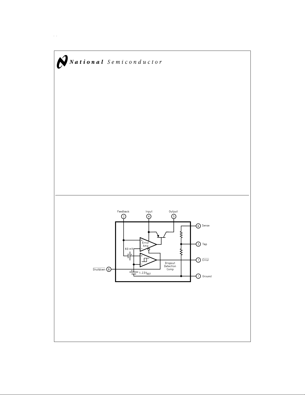
Block Diagram
Features
n Ultra low dropout voltage
n Guaranteed 200 mA output current
n SO-8 and mini-SO8 surface mount packages
<
n
1 µA quiescent current when shutdown
n Low ground pin current at all loads
n 0.5%output voltage accuracy (“A” grade)
n High peak current capability (400 mA typical)
n Wide supply voltage range (16V max)
n Overtemperature/overcurrent protection
n −40˚C to +125˚C junction temperature range
Applications
n Cellular Phone
n Palmtop/Laptop Computer
n Camcorder, Personal Stereo, Camera
DS012935-1
VIP™is a trademark ofNational Semiconductor Corporation.
© 1999 National Semiconductor Corporation DS012935 www.national.com
Page 2
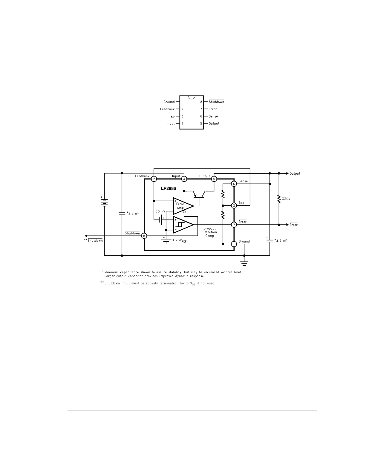
Connection Diagram and Ordering Information
Mini SO-8 Package Type MM: See NS Package Drawing Number MUA08A
SO-8 Package Type M: See NS Package Drawing Number M08A
For ordering information, refer to Table 1 of this document.
Basic Application Circuits
Application Using Internal Resistive Divider
Surface Mount Packages:
DS012935-2
Top View
www.national.com 2
DS012935-3
Page 3
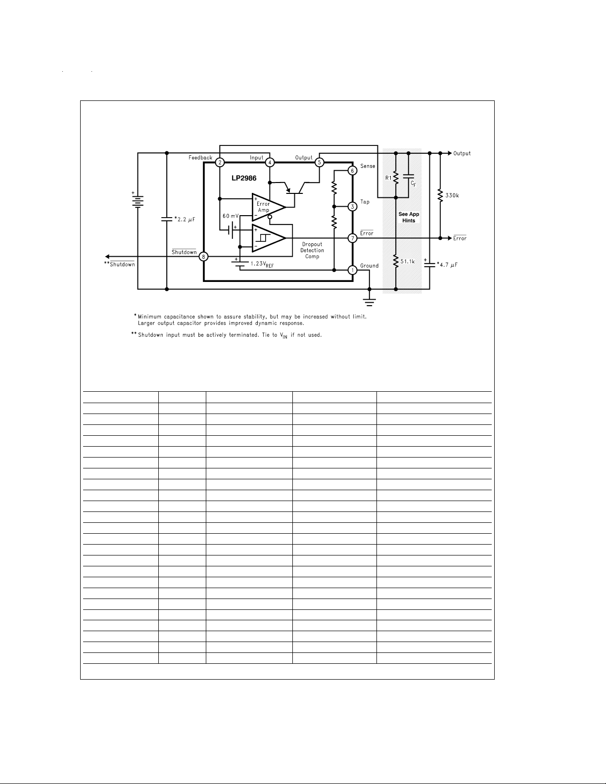
Basic Application Circuits (Continued)
Application Using External Divider
Ordering Information
TABLE 1. Package Marking and Ordering Information
Output Voltage Grade Order Information Package Marking Supplied as:
5 A LP2986AIMMX-5.0 L41A 3.5k Units on Tape and Reel
5 A LP2986AIMM-5.0 L41A 250 Units on Tape and Reel
5 STD LP2986IMMX-5.0 L41B 3.5k Units on Tape and Reel
5 STD LP2986IMM-5.0 L41B 250 Units on Tape and Reel
3.3 A LP2986AIMMX-3.3 L40A 3.5k Units on Tape and Reel
3.3 A LP2986AIMM-3.3 L40A 250 Units on Tape and Reel
3.3 STD LP2986IMMX-3.3 L40B 3.5k Units on Tape and Reel
3.3 STD LP2986IMM-3.3 L40B 250 Units on Tape and Reel
3.0 A LP2986AIMMX-3.0 L39A 3.5k Units on Tape and Reel
3.0 A LP2986AIMM-3.0 L39A 250 Units on Tape and Reel
3.0 STD LP2986IMMX-3.0 L39B 3.5k Units on Tape and Reel
3.0 STD LP2986IMM-3.0 L39B 250 Units on Tape and Reel
5 A LP2986AIMX-5.0 2986AIM5.0 2.5k Units on Tape and Reel
5 A LP2986AIM-5.0 2986AIM5.0 Shipped in Anti-Static Rails
5 STD LP2986IMX-5.0 2986IM5.0 2.5k Units on Tape and Reel
5 STD LP2986IM-5.0 2986IM5.0 Shipped in Anti-Static Rails
3.3 A LP2986AIMX-3.3 2986AIM3.3 2.5k Units on Tape and Reel
3.3 A LP2986AIM-3.3 2986AIM3.3 Shipped in Anti-Static Rails
3.3 STD LP2986IMX-3.3 2986IM3.3 2.5k Units on Tape and Reel
3.3 STD LP2986IM-3.3 2986IM3.3 Shipped in Anti-Static Rails
3.0 A LP2986AIMX-3.0 2986AIM3.0 2.5k Units on Tape and Reel
3.0 A LP2986AIM-3.0 2986AIM3.0 Shipped in Anti-Static Rails
3.0 STD LP2986IMX-3.0 2986IM3.0 2.5k Units on Tape and Reel
3.0 STD LP2986IM-3.0 2986IM3.0 Shipped in Anti-Static Rails
DS012935-4
www.national.com3
Page 4
Absolute Maximum Ratings (Note 1)
If Military/Aerospace specified devices are required,
please contact the National Semiconductor Sales Office/
Distributors for availability and specifications.
Storage Temperature Range −65˚C to +150˚C
Operating Junction
Temperature Range −40˚C to +125˚C
Lead Temperature
(Soldering, 5 seconds) 260˚C
Input Supply Voltage
(Operating) 2.1V to +16V
Shutdown Pin −0.3V to +16V
Feedback Pin −0.3V to +5V
Output Voltage
(Survival) (Note 4) −0.3V to +16V
I
(Survival) Short Circuit Protected
OUT
Input-Output Voltage
(Survival) (Note 5) −0.3V to +16V
ESD Rating (Note 2) 2 kV
Power Dissipation (Note 3) Internally Limited
Input Supply Voltage
(Survival) −0.3V to +16V
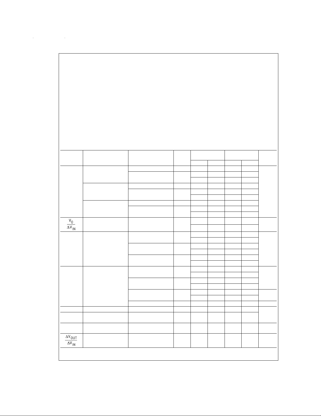
Electrical Characteristics
Limits in standard typeface are for TJ= 25˚C, and limits in boldface type apply over the full operating temperature range. Unless otherwise specified: VIN=VO(NOM) + 1V, IL= 1 mA, C
Symbol Parameter Conditions Typical
V
O
Output Voltage
(5.0V Versions)
0.1 mA
<
<
I
L
Output Voltage
(3.3V Versions)
0.1 mA
<
<
I
L
Output Voltage
(3.0V Versions)
Output Voltage Line
Regulation
V
IN–VO
I
GND
I
(PK) Peak Output Current V
O
(MAX) Short Circuit Current RL= 0 (Steady State)
I
O
e
n
Dropout Voltage
(Note 7)
Ground Pin Current IL= 100 µA
Output Noise Voltage
(RMS)
Ripple Rejection f = 1 kHz, C
<
0.1 mA
<
I
L
VO(NOM) + 1V ≤ VIN≤
16V
IL= 100 µA
=75mA
I
L
I
= 200 mA
L
I
=75mA
L
I
= 200 mA
L
<
0.3V 0.05 1.5 1.5 µA
V
S/D
≥ VO(NOM) − 5
OUT
(Note 11)
BW = 300 Hz to 50
OUT
=10µF
OUT
kHz, C
= 4.7 µF, CIN= 2.2 µF, V
OUT
200 mA
200 mA
200 mA
0.007
%
=10µF
= 2V.
S/D
LM2986AI-X.X
(Note 6)
LM2986I-X.X
(Note 6)
Min Max Min Max
5.0 4.975 5.025 4.950 5.050
4.960 5.040 4.920 5.080
5.0
4.910 5.090 4.860 5.140
3.3 3.283 3.317 3.267 3.333
3.274 3.326 3.247 3.353
3.3
3.241 3.359 3.208 3.392
3.0 2.985 3.015 2.970 3.030
2.976 3.024 2.952 3.048
3.0
2.946 3.054 2.916 3.084
0.014 0.014
0.032 0.032
1
90
180
100
500
1
2.0 2.0
3.5 3.5
120 120
170 170
230 230
350 350
120 120
150 150
800 800
1400 1400
2.1 2.1
3.7 3.7
400 250 250
400
160 µV(RMS)
65 dB
Units
V
%
/V
mV
µA
mA
mA
www.national.com 4
Page 5
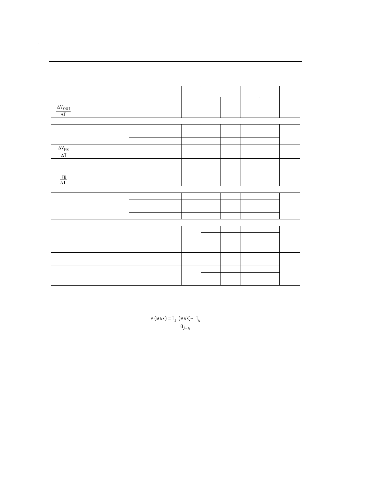
Electrical Characteristics (Continued)
Limits in standard typeface are for TJ= 25˚C, and limits in boldface type apply over the full operating temperature range. Unless otherwise specified: VIN=VO(NOM) + 1V, IL= 1 mA, C
Symbol Parameter Conditions Typical
Output Voltage
(Note 9)
Temperature Coefficient
FEEDBACK PIN
V
FB
Feedback Pin Voltage
(Note 10) 1.23 1.19 1.28 1.18 1.29
FB Pin Voltage
(Note 9)
Temperature Coefficient
I
FB
Feedback Pin Bias
Current
FB Pin Bias Current
IL= 200 mA
(Note 9)
Temperature Coefficient
SHUTDOWN INPUT
V
S/D
I
S/D
S/D Input Voltage
(Note 8)
S/D Input Current V
VH= O/P ON 1.4 1.6 1.6
= O/P OFF 0.55 0.18 0.18
V
L
=0 0 −1 −1
S/D
=5V 5 15 15
V
S/D
ERROR COMPARATOR
I
OH
V
OL
V
THR
(MAX)
V
THR
(MIN)
Output “HIGH” Leakage VOH= 16V
Output “LOW” Voltage VIN=VO(NOM) − 0.5V,
(COMP) = 300 µA
I
O
Upper Threshold
Voltage
Lower Threshold
Voltage
HYST Hysteresis 2.0
Note 1: Absolute Maximum Ratings indicate limits beyond which damage to the component may occur. Electrical specifications do not apply when operating the device outside of its rated operating conditions.
Note 2: The ESD rating of the Feedback pin is 500V and the Tap pin is 1.5 kV.
Note 3: The maximum allowable power dissipation is a function of the maximum junction temperature, T
and the ambient temperature, T
. The maximum allowable power dissipation at any ambient temperature is calculated using:
A
= 4.7 µF, CIN= 2.2 µF, V
OUT
20 ppm/˚C
1.23
20 ppm/˚C
150
0.1 nA/˚C
0.01
150
−4.6
−6.6
= 2V.
S/D
LM2986AI-X.X
(Note 6)
LM2986I-X.X
(Note 6)
Min Max Min Max
1.21 1.25 1.20 1.26
330 330
760 760
11
22
220 220
350 350
−5.5 −3.5 −5.5 −3.5
−7.7 −2.5 −7.7 −2.5
−8.9 −4.9 −8.9 −4.9
−13.0 −3.3 −13.0 −3.3
(MAX), the junction-to-ambient thermal resistance, θ
J
%
Units
V1.20 1.26 1.19 1.27
nA
V
µA
µA
mV
V
OUT
J−A
,
The value of θ
excessive die temperature, and the regulator will go into thermal shutdown.
Note 4: If used in a dual-supply system where the regulator load is returned to a negative supply, the LM2986 output must be diode-clamped to ground.
Note 5: The output PNP structure contains a diode between the V
on this diode and may induce a latch-up mode which can damage the part (see Application Hints).
Note 6: Limits are 100%production tested at 25˚C. Limits over the operating temperature range are guaranteed through correlation using Statistical Quality Control
(SQC) methods. The limits are used to calculate National’s Average Outgoing Quality Level (AOQL).
Note 7: Dropout voltage is defined as the input to output differential at which the output voltage drops 100 mV below the value measured with a 1V differential.
Note 8: Toprevent mis-operation, the Shutdown input must be driven by a signal that swings above V
Application Hints).
Note 9: Temperature coefficient is defined as the maximum (worst-case) change divided by the total temperature range.
Note 10: V
Note 11: See Typical Performance Characteristics curves.
for the SO-8 (M) package is 160˚C/W,and the mini SO-8 (MM) package is 200˚C/W. Exceeding the maximum allowable power dissipation will cause
J−A
and V
terminals that is normally reverse-biased. Forcing the output above the input will turn
OUT
and below VLwith a slew rate not less than 40 mV/µs (see
H
≤ V
≤ (VIN− 1), 2.5V ≤ VIN≤ 16V, 100 µA≤ IL≤ 200 mA, TJ≤ 125˚C.
FB
OUT
IN
www.national.com5
Page 6

Typical PerformanceCharacteristics Unless otherwise specified: T
C
= 2.2 µF, S/D is tied to VIN,VIN=VO(NOM) + 1V, IL= 1 mA.
IN
vs Temperature
V
OUT
Dropout Voltage vs Temperature
= 25˚C, C
A
OUT
= 4.7 µF,
DS012935-8
Dropout Voltage vs Load Current
DS012935-10
Ground Pin Current vs Temperature and Load
DS012935-9
Dropout Characteristics
DS012935-13
Ground Pin Current vs Load Current
DS012935-12
www.national.com 6
DS012935-11
Page 7

Typical Performance Characteristics Unless otherwise specified: T
C
= 2.2 µF, S/D is tied to VIN,VIN=VO(NOM) + 1V, IL= 1 mA. (Continued)
IN
= 25˚C, C
A
OUT
= 4.7 µF,
Input Current vs V
IN
Load Transient Response
Line Transient Response
DS012935-14
DS012935-16
Input Current vs V
IN
Load Transient Response
Line Transient Response
DS012935-15
DS012935-17
DS012935-18
DS012935-20
www.national.com7
Page 8

Typical Performance Characteristics Unless otherwise specified: T
C
= 2.2 µF, S/D is tied to VIN,VIN=VO(NOM) + 1V, IL= 1 mA. (Continued)
IN
= 25˚C, C
A
OUT
= 4.7 µF,
Turn-On Waveform
Short Circuit Current
DS012935-21
DS012935-24
Turn-Off Waveform
DS012935-23
Short Circuit Current
DS012935-25
Short Circuit Current vs Output Voltage
DS012935-26
www.national.com 8
Instantaneous Short Circuit Current vs Temperature
DS012935-27
Page 9

Typical Performance Characteristics Unless otherwise specified: T
C
= 2.2 µF, S/D is tied to VIN,VIN=VO(NOM) + 1V, IL= 1 mA. (Continued)
IN
= 25˚C, C
A
OUT
= 4.7 µF,
DC Load Regulation
Feedback Bias Current vs Temperature
Shutdown Voltage vs Temperature
DS012935-28
DS012935-30
Feedback Bias Current vs Load
DS012935-29
Shutdown Pin Current vs Shutdown Pin Voltage
DS012935-31
Input to Output Leakage vs Temperature
DS012935-32
DS012935-37
www.national.com9
Page 10

Typical Performance Characteristics Unless otherwise specified: T
C
= 2.2 µF, S/D is tied to VIN,VIN=VO(NOM) + 1V, IL= 1 mA. (Continued)
IN
= 25˚C, C
A
OUT
= 4.7 µF,
Output Noise Density
Output Impedance vs Frequency
DS012935-34
DS012935-36
Output Impedance vs Frequency
DS012935-35
Ripple Rejection
DS012935-33
www.national.com 10
Page 11

Application Hints
EXTERNAL CAPACITORS
Like any low-dropout regulator, external capacitors are required to assure stability.These capacitors mustbe correctly
selected for proper performance.
INPUT CAPACITOR: An input capacitor (≥ 2.2 µF) is re-
quired between the LP2986 input and ground(amount of capacitance may be increased without limit).
This capacitor must be located a distance of not more than
0.5” from the input pin and returned to a clean analog
ground. Any good quality ceramic or tantalum may be used
for this capacitor.
OUTPUT CAPACITOR: The output capacitor must meet the
requirement for minimum amount of capacitance and also
have an appropriate E.S.R. (equivalent series resistance)
value.
Curves are provided which show the allowable ESR range
as a function of load current for various output voltages and
capacitor values (see ESR curves below).
ESR Curves For 5V Output
DS012935-6
ESR Curves For 2.5V Output
DS012935-7
IMPORTANT
the stable region
the application
The minimum required amount of output capacitance is
4.7 µF. Output capacitor size can be increased without limit.
It is important to remember that capacitor tolerance and
variation with temperature must be taken into consideration
: The output capacitor must maintain its ESR in
over the full operating temperature range of
to assure stability.
when selecting an output capacitor so that the minimum required amount of output capacitance is providedover the full
operating temperature range. A good Tantalumcapacitor will
show very little variation with temperature, but a ceramic
may not be as good (see next section).
CAPACITOR CHARACTERISTICS
TANTALUM: The best choice for size, cost, and perfor-
mance are solid tantalum capacitors. Available from many
sources, their typical ESRis very close to the ideal value required on the output of many LDO regulators.
Tantalums also have good temperature stability: a 4.7 µF
was tested and showed only a 10%decline in capacitance
as the temperature was decreased from +125˚C to −40˚C.
The ESR increased only about 2:1 over the same range of
temperature.
However,it should be noted that the increasing ESR at lower
temperatures present in all tantalums can cause oscillations
when marginal quality capacitors are used (where the ESR
of the capacitor is near the upper limit of the stability range at
room temperature).
CERAMIC: For a given amount of a capacitance, ceramics
are usually larger and more costly than tantalums.
Be warned that the ESR of a ceramic capacitor can be low
enough to cause instability:a 2.2 µF ceramic was measured
and found to have an ESR of about 15 mΩ.
If a ceramic capacitor is to be used on the LP2986 output, a
1Ω resistor should be placed in series with the capacitor to
provide a minimum ESR for the regulator.
Another disadvantage of ceramic capacitors is that their capacitance varies a lot with temperature:
Large ceramic capacitors are typically manufactured with the
Z5U temperature characteristic, which results in the capacitance dropping by a 50%as the temperature goes from 25˚C
to 80˚C.
This means you have to buy a capacitor with twice the minimum C
to assure stable operation up to 80˚C.
OUT
ALUMINUM: The large physicalsize of aluminum electrolytics makes them unattractive for use with the LP2986. Their
ESR characteristics are also not well suited to the requirements of LDO regulators.
The ESR of an aluminum electrolytic is higher than a tantalum, and it also varies greatly with temperature.
A typical aluminum electrolytic can exhibit an ESR increase
of 50X when going from 20˚C to −40˚C. Also, some aluminum electrolytics can not be used below −25˚C because the
electrolyte will freeze.
USING AN EXTERNAL RESISTIVE DIVIDER
The LP2986 output voltage can be programmed using an external resistive divider (see Basic Application Circuits).
The resistor connected between the Feedback pin and
ground should be 51.1k. The value for the other resistor (R1)
connected between the Feedback pin andthe regulatedoutput is found using the formula:
V
= 1.23 x (1 + R1/51.1k)
OUT
It should be noted that the 25 µAof current flowing through
the external divider is approximately equal to the current
saved by not connecting the internal divider, which means
the quiescent current is not increased by using external resistors.
www.national.com11
Page 12

Application Hints (Continued)
A lead compensation capacitor (C
place a zero in the loop response at about 50 kHz. The value
for C
can be found using:
F
= 1/(2π x R1 x 50k)
C
F
A good quality capacitor must be used for C
the value isaccurate and does not change significantly over
temperature. Mica or ceramic capacitors can be used, assuming a tolerance of
±
20%or better is selected.
If a ceramic is used, select one with a temperature coefficient of NPO, COG, Y5P,or X7R. Capacitor typesZ5U, Y5V,
and Z4V can not be used because their value varies more
that 50%over the −25˚C to +85˚C temperature range.
SHUTDOWN INPUT OPERATION
The LP2986 is shut off by driving the Shutdown input low,
and turned on by pulling it high. If this feature is not to be
used, the Shutdown input should be tied to V
regulator output on at all times.
To assure proper operation, the signal source used to drive
the Shutdown input must be able to swing above and below
the specified turn-on/turn-off voltage thresholds listed as V
and VL, respectively (see Electrical Characteristics).
) must also be used to
F
to ensure that
F
to keep the
IN
It is also importantthat theturn-on (andturn-off) voltage signals applied to the Shutdowninput havea slew ratewhich is
not less than 40 mV/µs.
CAUTION:
the regulator output statecan not be guaranteed
if a slow-moving AC (or DC) signal is applied that is in the
range between V
and VL.
H
REVERSE INPUT-OUTPUT VOLTAGE
The PNP power transistor used as the pass element in the
LP2986 has an inherentdiode connected between the regulator output and input.
During normal operation (where the input voltage is higher
than the output) this diode is reverse-biased.
However, if the output is pulled above the input, this diode
will turn ON and current will flow into the regulator output.
In such cases, a parasitic SCR can latch which will allow a
high current to flow into V
can damage the part.
(and out the ground pin), which
IN
In any application where theoutput may bepulled abovethe
input, an external Schottky diode must be connected from
V
to V
IN
verse voltage across the LP2986 to 0.3V (see Absolute
H
Maximum Ratings).
(cathode on VIN, anode on V
OUT
), to limit the re-
OUT
www.national.com 12
Page 13

Physical Dimensions inches (millimeters) unless otherwise noted
8-Lead Mini-Small Outline Molded Package, JEDEC
NS Package Number MUA08A
www.national.com13
Page 14

Physical Dimensions inches (millimeters) unless otherwise noted (Continued)
8-Lead (0.150” Wide) Molded Small Outline Package, JEDEC
NS Package Number M08A
LIFE SUPPORT POLICY
NATIONAL’S PRODUCTS ARE NOT AUTHORIZED FOR USE AS CRITICAL COMPONENTS IN LIFE SUPPORT
DEVICES OR SYSTEMS WITHOUT THE EXPRESS WRITTEN APPROVAL OF THE PRESIDENT OF NATIONAL
SEMICONDUCTOR CORPORATION. As used herein:
1. Life support devices or systems are devices or
systems which, (a) are intended for surgical implant
into the body, or (b) support or sustain life, and
whose failure to perform when properly used in
accordance with instructions for use provided in the
labeling, can be reasonably expected to result in a
LP2986 Micropower, 200 mA Ultra Low-Dropout Fixed or Adjustable Voltage Regulator
significant injury to the user.
National Semiconductor
Corporation
Americas
Tel: 1-800-272-9959
Fax: 1-800-737-7018
Email: support@nsc.com
www.national.com
National Semiconductor
Europe
Fax: +49 (0) 1 80-530 85 86
Email: europe.support@nsc.com
Deutsch Tel: +49 (0) 1 80-530 85 85
English Tel: +49 (0) 1 80-532 78 32
Français Tel: +49 (0) 1 80-532 93 58
Italiano Tel: +49 (0) 1 80-534 16 80
2. A critical component is any component of a life
support device or system whose failure to perform
can be reasonably expected to cause the failure of
the life support device or system, or to affect its
safety or effectiveness.
National Semiconductor
Asia Pacific Customer
Response Group
Tel: 65-2544466
Fax: 65-2504466
Email: sea.support@nsc.com
National Semiconductor
Japan Ltd.
Tel: 81-3-5639-7560
Fax: 81-3-5639-7507
National does not assume any responsibility for use of any circuitry described, no circuit patent licenses are implied and National reserves the right at any time without notice to change said circuitry and specifications.
 Loading...