

Datasheet LP2981IM5X-3.3, LP2981IM5X-3.0, LP2981IM5X-2.5, LP2981IM5-5.0, LP2981AIM5X-5.0 Datasheet (NSC)
...
LP2981
Micropower 100 mA Ultra Low-Dropout Regulator
General Description
The LP2981 is a 100 mA, fixed-output voltage regulator designed specifically to meet the requirements of
battery-powered applications.
Using an optimized VIP
™
(Vertically Integrated PNP) process, the LP2981 delivers unequaled performance in all
specifications critical to battery-powered designs:
Dropout Voltage. Typically 200 mV
@
100 mA load, and
7mV
@
1 mA load.
Ground Pin Current. Typically 600 µA
@
100 mA load, and
80 µA
@
1 mA load.
Sleep Mode. Less than 1 µA quiescent current when ON/
OFF pin is pulled low.
Smallest Possible Size. SOT-23and micro SMD packages
use an absolute minimum board space.
Precision Output. 0.75% tolerance output voltages available (A grade).
Eleven voltage options, from 2.5V to 5.0V, are available as
standard products.
Features
n Ultra low dropout voltage
n Output voltage accuracy 0.75% (A Grade)
n Guaranteed 100 mA output current
n Smallest possible size (SOT-23, micro SMD package)
n
<
1 µA quiescent current when shutdown
n Low ground pin current at all load currents
n High peak current capability (300 mA typical)
n Wide supply voltage range (16V max)
n Fast dynamic response to line and load
n Low Z
OUT
over wide frequency range
n Overtemperature/overcurrent protection
n −40˚C to +125˚C junction temperature range
Applications
n Cellular Phone
n Palmtop/Laptop Computer
n Personal Digital Assistant (PDA)
n Camcorder, Personal Stereo, Camera
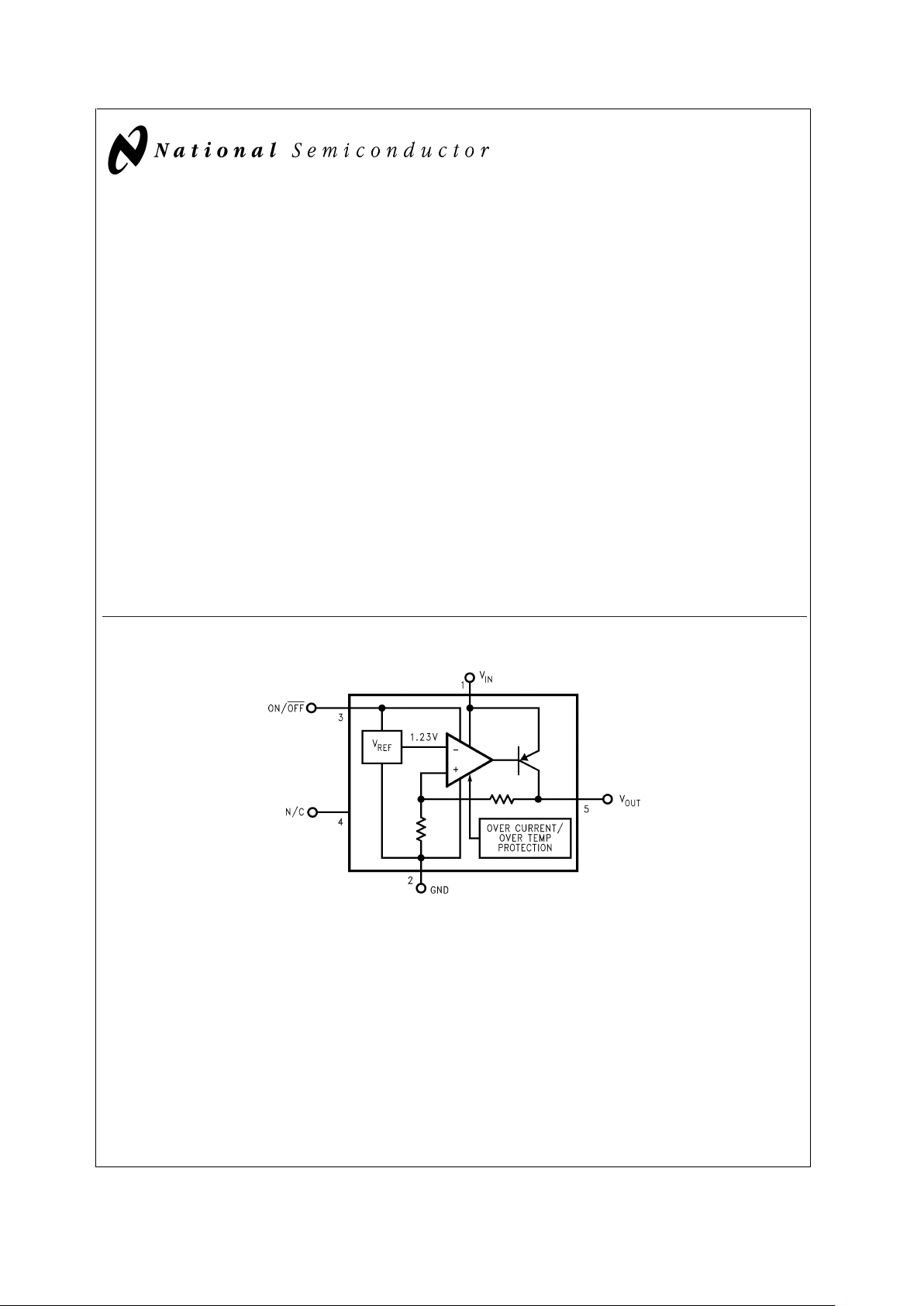
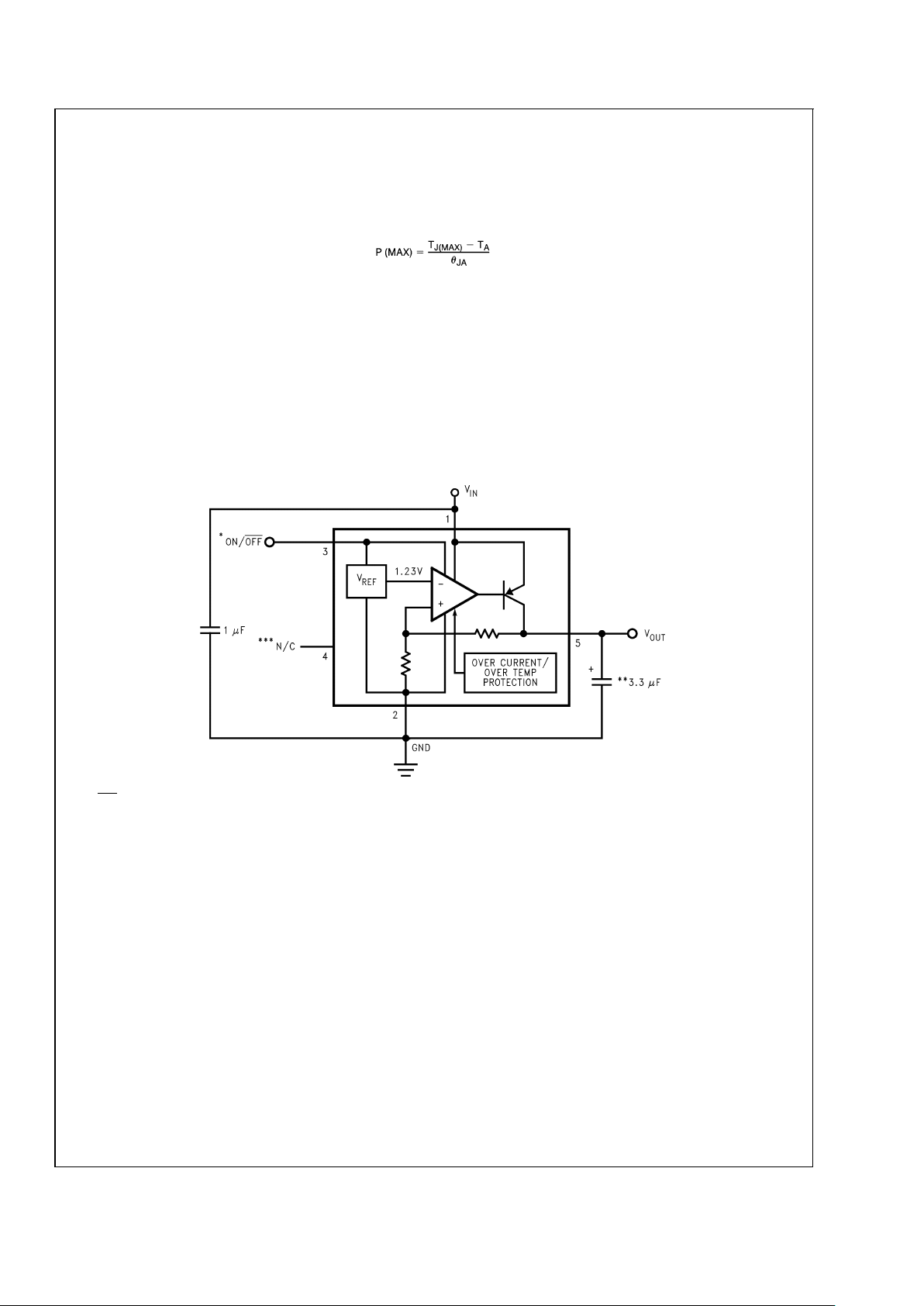
Block Diagram
VIP™is a trademark of National Semiconductor Corporation.
DS012506-1
March 2000
LP2981 Micropower 100 mA Ultra Low-Dropout Regulator
© 2000 National Semiconductor Corporation DS012506 www.national.com
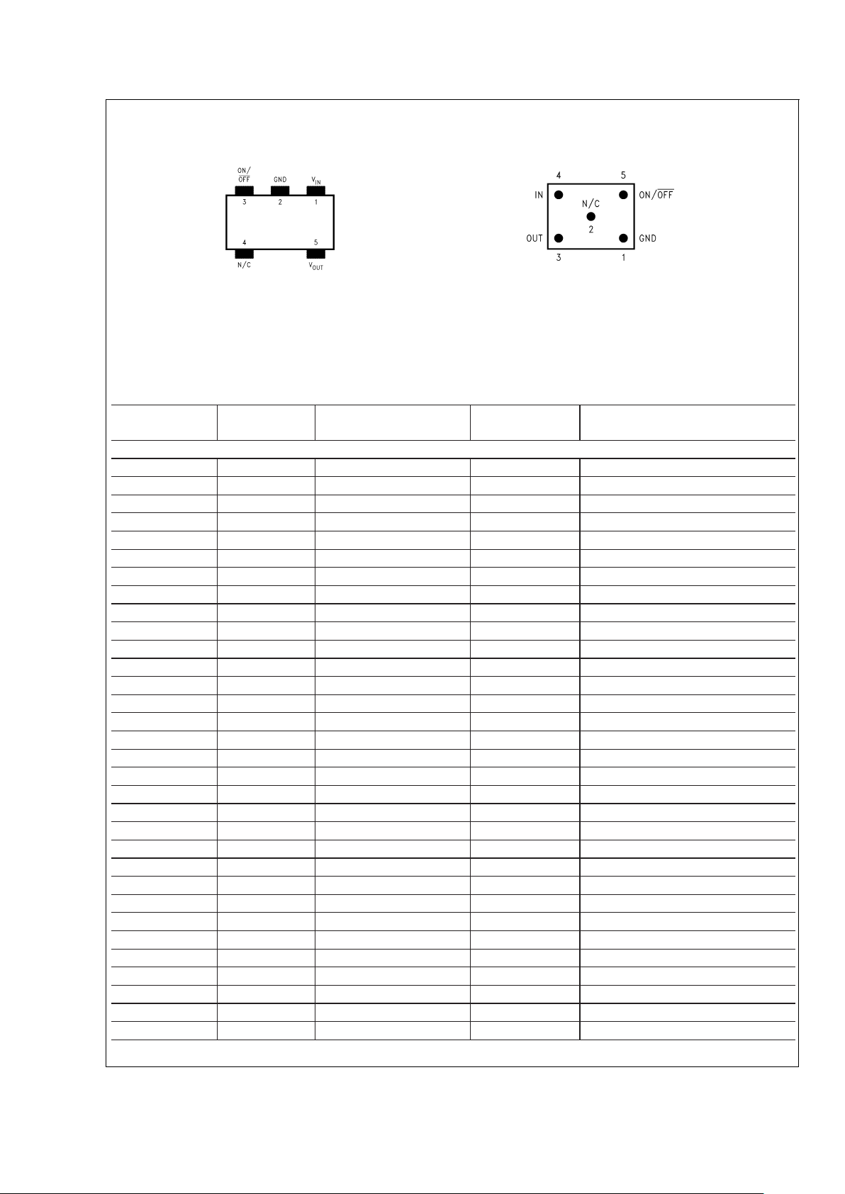
Connection Diagrams
Ordering Information
TABLE 1. Package Marking and Order Information
Output Voltage
(V)
Grade Order Information Package
Marking
Supplied as:
5-Lead Small Outline Package (M5)
2.5 A LP2981AIM5X-2.5 L0CA 3000 Units on Tape and Reel
2.5 A LP2981AIM5-2.5 L0CA 1000 Units on Tape and Reel
2.5 STD LP2981IM5X-2.5 L0CB 3000 Units on Tape and Reel
2.5 STD LP2981IM5-2.5 L0CB 1000 Units on Tape and Reel
2.7 A LP2981AIM5X-2.7 L0DA 3000 Units on Tape and Reel
2.7 A LP2981AIM5-2.7 L0DA 1000 Units on Tape and Reel
2.7 STD LP2981IM5X-2.7 L0DB 3000 Units on Tape and Reel
2.7 STD LP2981IM5-2.7 L0DB 1000 Units on Tape and Reel
2.8 A LP2981AIM5X-2.8 L77A 3000 Units on Tape and Reel
2.8 A LP2981AIM5-2.8 L77A 1000 Units on Tape and Reel
2.8 STD LP2981IM5X-2.8 L77B 3000 Units on Tape and Reel
2.8 STD LP2981IM5-2.8 L77B 1000 Units on Tape and Reel
2.9 A LP2981AIM5X-2.9 L0VA 3000 Units on Tape and Reel
2.9 A LP2981AIM5-2.9 L0VA 1000 Units on Tape and Reel
2.9 STD LP2981IM5X-2.9 L0VB 3000 Units on Tape and Reel
2.9 STD LP2981IM5-2.9 L0VB 1000 Units on Tape and Reel
3.0 A LP2981AIM5X-3.0 L05A 3000 Units on Tape and Reel
3.0 A LP2981AIM5-3.0 L05A 1000 Units on Tape and Reel
3.0 STD LP2981IM5X-3.0 L05B 3000 Units on Tape and Reel
3.0 STD LP2981IM5-3.0 L05B 1000 Units on Tape and Reel
3.1 A LP2981AIM5X-3.1 L38A 3000 Units on Tape and Reel
3.1 A LP2981AIM5-3.1 L38A 1000 Units on Tape and Reel
3.1 STD LP2981IM5X-3.1 L38B 3000 Units on Tape and Reel
3.1 STD LP2981IM5-3.1 L38B 1000 Units on Tape and Reel
3.2 A LP2981AIM5X-3.2 L35A 3000 Units on Tape and Reel
3.2 A LP2981AIM5-3.2 L35A 1000 Units on Tape and Reel
3.2 STD LP2981IM5X-3.2 L35B 3000 Units on Tape and Reel
3.2 STD LP2981IM5-3.2 L35B 1000 Units on Tape and Reel
3.3 A LP2981AIM5X-3.3 L04A 3000 Units on Tape and Reel
3.3 A LP2981AIM5-3.3 L04A 1000 Units on Tape and Reel
3.3 STD LP2981IM5X-3.3 L04B 3000 Units on Tape and Reel
3.3 STD LP2981IM5-3.3 L04B 1000 Units on Tape and Reel
5-Lead Small Outline Package (M5)
DS012506-2
Top View
See NS Package Number MF05A
For ordering information see
Table 1
micro SMD, 5 Bump Package (BPA05)
DS012506-50
Bottom View
See NS Package Number BPA05
LP2981
www.national.com 2
Ordering Information (Continued)
TABLE 1. Package Marking and Order Information (Continued)
Output Voltage
(V)
Grade Order Information Package
Marking
Supplied as:
5-Lead Small Outline Package (M5)
3.6 A LP2981AIM5X-3.6 L0JA 3000 Units on Tape and Reel
3.6 A LP2981AIM5-3.6 L0JA 1000 Units on Tape and Reel
3.6 STD LP2981IM5X-3.6 L0JB 3000 Units on Tape and Reel
3.6 STD LP2981IM5-3.6 L0JB 1000 Units on Tape and Reel
3.8 A LP2981AIM5X-3.8 L36A 3000 Units on Tape and Reel
3.8 A LP2981AIM5-3.8 L36A 1000 Units on Tape and Reel
3.8 STD LP2981IM5X-3.8 L36B 3000 Units on Tape and Reel
3.8 STD LP2981IM5-3.8 L36B 1000 Units on Tape and Reel
4.0 A LP2981AIM5X-4.0 L0ZA 3000 Units on Tape and Reel
4.0 A LP2981AIM5-4.0 L0ZA 1000 Units on Tape and Reel
4.0 STD LP2981IM5X-4.0 L0ZB 3000 Units on Tape and Reel
4.0 STD LP2981IM5-4.0 L0ZB 1000 Units on Tape and Reel
4.7 A LP2981AIM5X-4.7 L0GA 3000 Units on Tape and Reel
4.7 A LP2981AIM5-4.7 L0GA 1000 Units on Tape and Reel
4.7 STD LP2981IM5X-4.7 L0GB 3000 Units on Tape and Reel
4.7 STD LP2981IM5-4.7 L0GB 1000 Units on Tape and Reel
5.0 A LP2981AIM5X-5.0 L03A 3000 Units on Tape and Reel
5.0 A LP2981AIM5-5.0 L03A 1000 Units on Tape and Reel
5.0 STD LP2981IM5X-5.0 L03B 3000 Units on Tape and Reel
5.0 STD LP2981IM5-5.0 L03B 1000 Units on Tape and Reel
micro SMD, 5 Bump Package (BPA05)
2.5 A LP2981AIBP-2.5 250 Units on Tape and Reel
2.5 A LP2981AIBPX-2.5 3000 Units on Tape and Reel
2.5 STD LP2981IBP-2.5 250 Units on Tape and Reel
2.5 STD LP2981IBPX-2.5 3000 Units on Tape and Reel
3.2 A LP2981AIBP-3.2 250 Units on Tape and Reel
3.2 A LP2981AIBPX-3.2 3000 Units on Tape and Reel
3.2 STD LP2981IBP-3.2 250 Units on Tape and Reel
3.2 STD LP2981IBPX-3.2 3000 Units on Tape and Reel
3.3 A LP2981AIBP-3.3 250 Units on Tape and Reel
3.3 A LP2981AIBPX-3.3 3000 Units on Tape and Reel
3.3 STD LP2981IBP-3.3 250 Units on Tape and Reel
3.3 STD LP2981IBPX-3.3 3000 Units on Tape and Reel
LP2981
www.national.com3
Absolute Maximum Ratings (Note 1)
If Military/Aerospace specified devices are required,
please contact the National Semiconductor Sales Office/
Distributors for availability and specifications.
Storage Temperature Range −65˚C to +150˚C
Operating Junction Temperature
Range −40˚C to +125˚C
Lead Temperature
(Soldering, 5 sec.) 260˚C
ESD Rating (Note 2) 2 kV
Power Dissipation (Note 3) Internally Limited
Input Supply Voltage (Survival) −0.3V to +16V
Input Supply Voltage (Operating) 2.1V to +16V
Shutdown Input Voltage (Survival) −0.3V to +16V
Output Voltage (Survival, (Note 4)) −0.3V to +9V
I
OUT
(Survival) Short Circuit Protected
Input-Output Voltage
(Survival, (Note 5)) −0.3V to +16V
Electrical Characteristics
Limits in standard typeface are for TJ= 25˚C, and limits in boldface type applyover the full operating temperature range. Unless otherwise specified: V
IN=VO(NOM)
+ 1V, CIN= 1 µF, IL= 1 mA, C
OUT
= 4.7 µF,V
ON/OFF
= 2V.
Symbol Parameter Conditions Typ LP2981AI-XX LP2981I-XX Units
(Note 6) (Note 6)
Min Max Min Max
∆V
O
Output Voltage
Tolerance
IL= 1mA −0.75 0.75 −1.25 1.25
%V
NOM
1mA<I
L
<
100 mA −1.0 1.0 −2.0 2.0
−2.5 2.5 −3.5 3.5
Output Voltage V
O(NOM)
+ 1V 0.007 0.014 0.014 %/V
Line Regulation ≤ V
IN
≤ 16V 0.032 0.032
V
IN–VO
Dropout Voltage IL=0 133mV
(Note 7) 55
I
L
= 1 mA 7 10 10
15 15
I
L
= 25 mA 70 100 100
150 150
I
L
= 100 mA 200 250 250
375 375
I
GND
Ground Pin Current IL= 0 65 95 95 µA
125 125
I
L
= 1 mA 80 110 110
170 170
I
L
= 25 mA 200 300 300
550 550
I
L
= 100 mA 600 800 800
1500 1500
V
ON/OFF
<
0.3V 0.01 0.8 0.8
V
ON/OFF
<
0.15V 0.05 2 2
V
ON/OFF
ON/OFF Input Voltage High = O/P ON 1.4 1.6 1.6 V
(Note 8) Low = O/P OFF 0.50 0.15 0.15
I
ON/OFF
ON/OFF Input Current V
ON/OFF
= 0 0.01 −1 −1 µA
V
ON/OFF
=5V 5 15 15
I
O(PK)
Peak Output Current V
OUT
≥ V
O(NOM)
− 5% 400 150 150 mA
e
n
Output Noise BW = 300 Hz–50 kHz, 160 µV
Voltage (RMS) C
OUT
=10µF
Ripple Rejection f = 1 kHz 63 dB
C
OUT
=10µF
I
O(MAX)
Short Circuit Current RL= 0 (Steady State) 150 mA
(Note 9)
LP2981
www.national.com 4
Electrical Characteristics (Continued)
Note 1: Absolute maximum ratings indicate limits beyond which damage to the component may occur. Electrical specifications do not apply when operating the de-
vice outside of its rated operating conditions.
Note 2: The ESD rating of pins 3 and 4 is 1 kV.
Note 3: The maximum allowable power dissipation is a function of the maximum junction temperature, T
J(MAX)
, the junction-to-ambient thermal resistance, θJA, and
the ambient temperature, T
A
. The maximum allowable power dissipation at any ambient temperature is calculated using:
The value of θJAfor the SOT-23 package is 220˚C/W and the micro SMD package is 320˚C/W. Exceeding the maximum allowable power dissipation will cause excessive die temperature, and the regulator will go into thermal shutdown.
Note 4: If used in a dual-supply system where the regulator load is returned to a negative supply, the LP2981 output must be diode-clamped to ground.
Note 5: The output PNP structure contains a diode between the V
IN
and V
OUT
terminals that is normally reverse-biased. Reversing the polarity from VINto V
OUT
will turn on this diode (see Application Hints).
Note 6: Limits are 100% production tested at 25˚C. Limits over the operating temperature range are guaranteed through correlation using Statistical Quality Control
(SQC) methods. The limits are used to calculate National’s Average Outgoing Quality Level (AOQL).
Note 7: Dropout voltage is defined as the input to output differential at which the output voltage drops 100 mV below the value measured with a 1V differential.
Note 8: The ON/OFF inputs must be properly driven to prevent misoperation. For details, refer to Application Hints.
Note 9: See Typical Performance Characteristics curves.
Basic Application Circuit
DS012506-4
*
ON/OFF input must be actively terminated. Tie to VINif this function is not to be used.
**
Minimum Output Capacitance is shown to insure stability over full load current range. More capacitance provides superior dynamic performance and
additional stability margin (see Application Hints).
***
Do not make connections to this pin.
LP2981
www.national.com5

Typical Performance Characteristics Unless otherwise specified: T
A
= 25˚C, VIN=V
O(NOM)
+1V,
C
OUT
= 4.7 µF, CIN= 1 µF all voltage options, ON/OFF pin tied to VIN.
Output Voltage vs
Temperature
DS012506-6
Output Voltage vs
Temperature
DS012506-7
Output Voltage vs
Temperature
DS012506-8
Dropout Characteristics
DS012506-9
Dropout Characteristics
DS012506-10
Dropout Characteristics
DS012506-11
LP2981
www.national.com 6

Typical Performance Characteristics Unless otherwise specified: T
A
= 25˚C, VIN=V
O(NOM)
+ 1V,
C
OUT
= 4.7 µF, CIN= 1 µF all voltage options, ON/OFF pin tied to VIN. (Continued)
Dropout Voltage vs
Temperature
DS012506-12
Dropout Voltage vs
Load Current
DS012506-13
Ground Pin Current vs
Temperature
DS012506-14
Ground Pin Current vs
Load Current
DS012506-15
Input Current vs V
IN
DS012506-16
Input Current vs V
IN
DS012506-17
LP2981
www.national.com7
Typical Performance Characteristics Unless otherwise specified: T
A
= 25˚C, VIN=V
O(NOM)
+ 1V,
C
OUT
= 4.7 µF, CIN= 1 µF all voltage options, ON/OFF pin tied to VIN. (Continued)
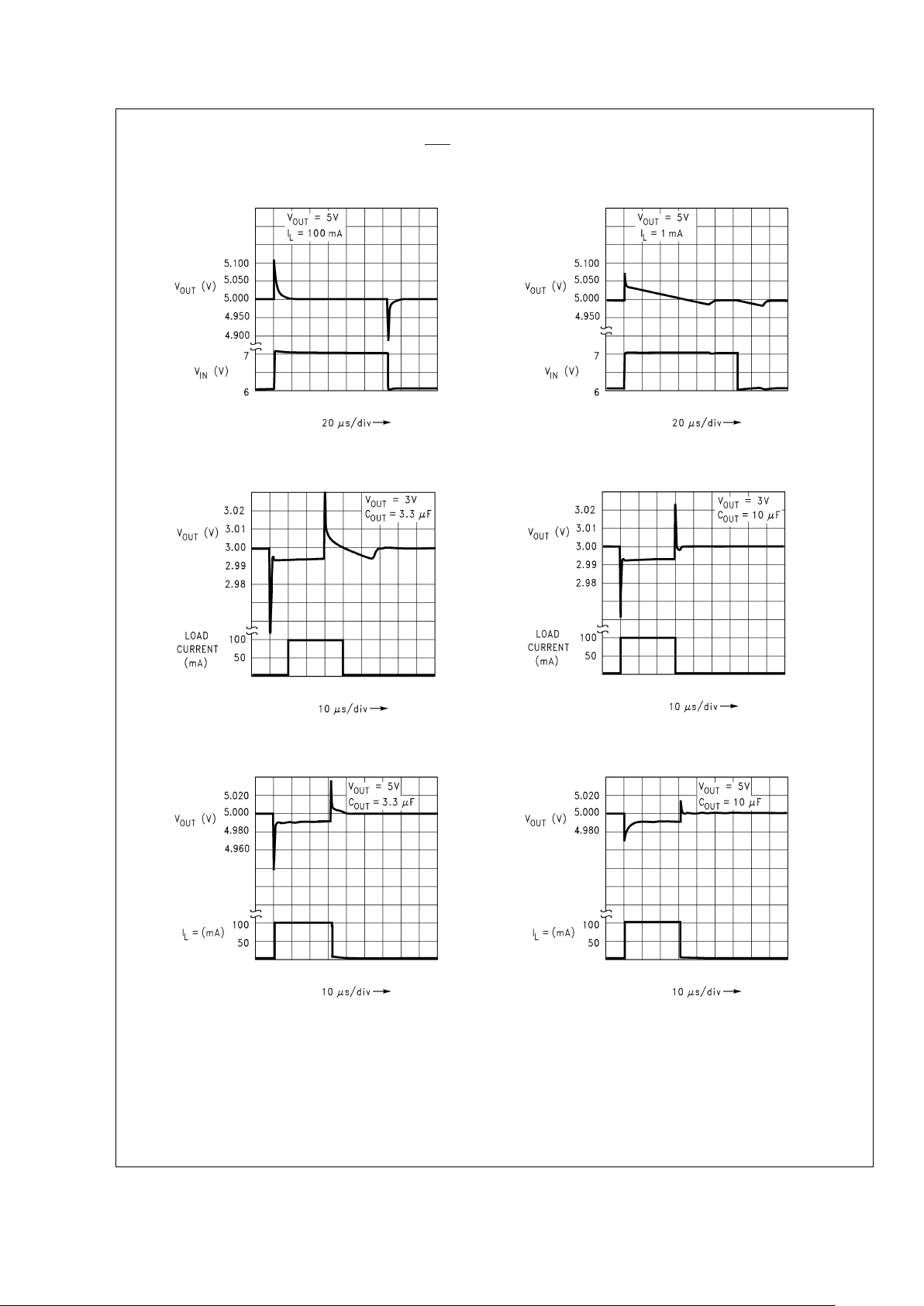
Line Transient Response
DS012506-18
Line Transient Response
DS012506-19
Load Transient Response
DS012506-20
Load Transient Response
DS012506-21
Load Transient Response
DS012506-22
Load Transient Response
DS012506-23
LP2981
www.national.com 8

Typical Performance Characteristics Unless otherwise specified: T
A
= 25˚C, VIN=V
O(NOM)
+ 1V,
C
OUT
= 4.7 µF, CIN= 1 µF all voltage options, ON/OFF pin tied to VIN. (Continued)
Short Circuit Current
DS012506-24
Instantaneous Short Circuit
Current vs Temperature
DS012506-25
Short Circuit Current
DS012506-26
Instantaneous Short Circuit
Current vs Output Voltage
DS012506-27
Output Impedance vs
Frequency
DS012506-28
Ripple Rejection
DS012506-29
LP2981
www.national.com9

Typical Performance Characteristics Unless otherwise specified: T
A
= 25˚C, VIN=V
O(NOM)
+ 1V,
C
OUT
= 4.7 µF, CIN= 1 µF all voltage options, ON/OFF pin tied to VIN. (Continued)
Output Noise Density
DS012506-30
Output Impedance vs
Frequency
DS012506-31
Input to Output Leakage
vs Temperature
DS012506-32
Output Reverse Leakage vs
Temperature
DS012506-33
Turn-On Waveform
DS012506-34
Turn-Off Waveform
DS012506-35
LP2981
www.national.com 10

Typical Performance Characteristics Unless otherwise specified: T
A
= 25˚C, VIN=V
O(NOM)
+ 1V,
C
OUT
= 4.7 µF, CIN= 1 µF all voltage options, ON/OFF pin tied to VIN. (Continued)
Application Hints
EXTERNAL CAPACITORS
Like any low-dropout regulator, the external capacitors used
with the LP2981 must be carefully selected to assure regulator loop stability.
INPUT CAPACITOR: An input capacitor whose value is
≥ 1 µF is required with the LP2981 (amount of capacitance
can be increased without limit).
This capacitor must be located a distance of not more than
0.5" from the input pin of the LP2981 and returned to a clean
analog ground. Any good quality ceramic or tantalum can be
used for this capacitor.
OUTPUT CAPACITOR: The output capacitor must meet
both the requirement for minimum amount of capacitance
and E.S.R. (equivalent series resistance) value. Curves are
provided which show the allowable ESR range as a function
of load current for various output voltages and capacitor values (refer to
Figures 1, 2, 3, 4
).
IMPORTANT: The output capacitor must maintain its ESR in
the stable region over the full operating temperature range to
assure stability. Also, capacitor tolerance and variation with
temperature must be considered to assure the minimum
amount of capacitance is provided at all times.
This capacitor should be located not more than 0.5" from the
output pin of the LP2981 and returned to a clean analog
ground.
CAPACITOR CHARACTERISTICS
TANTALUM: Tantalum capacitors are the best choice for
use with the LP2981. Most good quality tantalums can be
used with the LP2981, but check the manufacturer’s data
sheet to be sure the ESR is in range.
It is important to remember that ESR increases at lower temperatures and a capacitor that is near the upper limit for stability at room temperature can cause instability when it gets
cold.
In applications which must operate at very low temperatures,
it may be necessary to parallel the output tantalum capacitor
with a ceramic capacitor to prevent the ESR from going up
too high (see next section for important information on ceramic capacitors).
CERAMIC: Ceramic capacitors are not recommended for
use at the output of the LP2981. This is because the ESR of
a ceramic can be low enough to go below the minimum
stable value for the LP2981.A 2.2 µF ceramic was measured
and found to have an ESR of about 15 mΩ, which is low
enough to cause oscillations.
If a ceramic capacitor is used on the output, a 1Ω resistor
should be placed in series with the capacitor.
ALUMINUM: Because of large physical size, aluminum electrolytics are not typically used with the LP2981. They must
meet the same ESR requirements over the operating temperature range, more difficult because of their steep increase
at cold temperature.
An aluminum electrolytic can exhibit an ESR increase of as
much as 50X when going from 20˚C to −40˚C. Also, some
aluminum electrolytics are not operational below −25˚C because the electrolyte can freeze.
ON/OFF Pin Current vs
V
ON/OFF
DS012506-36
ON/OFF Threshold
vs Temperature
DS012506-37
DS012506-38
FIGURE 1. 5V/3.3 µF ESR Curves
LP2981
www.national.com11

Application Hints (Continued)
REVERSE CURRENT PATH
The power transistor used in the LP2981 has an inherent diode connected between the regulator input and output (see
below).
If the output is forced above the input by more than a V
BE
,
this diode will become forward biased and current will flow
from the V
OUT
terminal to VIN.
This current must be limited to
<
100 mA to prevent damage
to the part.
The internal diode can also be turned on by abruptly step-
ping the input voltage to a value below the output voltage.
To prevent regulator mis-operation, a Schottky diode should
be used in any application where input/output voltage conditions can cause the internal diode to be turned on (see below).
As shown, the Schottky diode is connected in parallel with
the internal parasitic diode and prevents it from being turned
on by limiting the voltage drop across it to about 0.3V.
ON/OFF INPUT OPERATION
The LP2981 is shut off by pulling the ON/OFF input low,and
turned on by driving the input high. If this feature is not to be
used, the ON/OFF input should be tied to V
IN
to keep the
regulator on at all times (the ON/OFF input must not be left
floating).
To ensure proper operation, the signal source used to drive
the ON/OFF input must be able to swing above and below
the specified turn-on/turn-off voltage thresholds which guarantee an ON or OFF state (see Electrical Characteristics).
The ON/OFF signal may come from either a totem-pole output, or an open-collector output with pull-up resistor to the
LP2981 input voltage or another logic supply. The high-level
voltage may exceed the LP2981 input voltage, but must remain within the Absolute Maximum Ratings for the ON/OFF
pin.
It is also important that the turn-on/turn-off voltage signals
applied to the ON/OFF input have a slew rate which is
greater than 40 mV/µs.
Important: the regulator shutdown function will operate incorrectly if a slow-moving signal is applied to the ON/OFF input.
Micro SMD Mounting
The micro SMD package requires specific mounting techniques which are detailed in National Semiconductor Application Note
#
1112. Referring to the section
Surface Mount
Technology (SMT)Assembly Considerations
, it should be
noted that the pad style which must be used with the 5-pin
package is the NSMD (non-solder mask defined) type.
DS012506-39
FIGURE 2. 5V/10 µF ESR Curves
DS012506-40
FIGURE 3. 3V/3.3 µF ESR Curves
DS012506-42
FIGURE 4. 3V/10 µF ESR Curves
DS012506-41
DS012506-43
LP2981
www.national.com 12

Application Hints (Continued)
For best results during assembly, alignment ordinals on the
PC board may be used to facilitate placement of the micro
SMD device.
Micro SMD Light Sensitivity
Exposing the micro SMD device to direct sunlight will cause
misoperation of the device. Light sources such as Halogen
lamps can also affect electrical performance if brought near
to the device.
The wavelenghts which have the most detrimental effect are
reds and infra-reds, which means that the fluorescent lighting used inside most buildings has very little effect on performance. A micro SMD test board was brought to within 1 cm
of a fluorescent desk lamp and the effect on the regulated
output voltage was negligible, showing a deviation of less
than 0.1% from nominal.
LP2981
www.national.com13

Physical Dimensions inches (millimeters) unless otherwise noted
5-Lead Small Outline Package (M5)
NS Package Number MF05A
For Order Numbers, refer to
Table 1
in the “Ordering Information” section of this document.
LP2981
www.national.com 14

Physical Dimensions inches (millimeters) unless otherwise noted (Continued)
NOTES: UNLESS OTHERWISE SPECIFIED
1. EPOXY COATING
2. 63Sn/37Pb EUTECTIC BUMP
3. RECOMMEND NON-SOLDER MASK DEFINED LANDING PAD.
4. PIN 1 IS ESTABLISHED BY LOWER LEFT CORNER WITH RESPECT TO TEXT ORIENTATION. REMAINING PINS ARE
NUMBERED COUNTER CLOCKWISE.
5. XXX IN DRAWING NUMBER REPRESENTS PACKAGE SIZE VARIATION WHERE X1 IS PACKAGE WIDTH, X2 IS PACKAGE LENGTH AND X3 IS PACKAGE HEIGHT.
6.NO JEDEC REGISTRATION AS OF AUG.1999.
micro SMD, 5 Bump Package (BPA05)
NS Package Number BPA05A
For Order Numbers, refer to
Table 1
in the “Order Information” section of this document.
The dimensions for X1, X2 and X3 are as given:
X1 = 0.930 +/− 0.030mm
X2 = 1.107 +/− 0.030mm
X3 = 0.850 +/− 0.050mm
LP2981
www.national.com15

Notes
LIFE SUPPORT POLICY
NATIONAL’S PRODUCTS ARE NOT AUTHORIZED FOR USE AS CRITICAL COMPONENTS IN LIFE SUPPORT
DEVICES OR SYSTEMS WITHOUT THE EXPRESS WRITTEN APPROVAL OF THE PRESIDENT AND GENERAL
COUNSEL OF NATIONAL SEMICONDUCTOR CORPORATION. As used herein:
1. Life support devices or systems are devices or
systems which, (a) are intended for surgical implant
into the body, or (b) support or sustain life, and
whose failure to perform when properly used in
accordance with instructions for use provided in the
labeling, can be reasonably expected to result in a
significant injury to the user.
2. A critical component is any component of a life
support device or system whose failure to perform
can be reasonably expected to cause the failure of
the life support device or system, or to affect its
safety or effectiveness.
National Semiconductor
Corporation
Americas
Tel: 1-800-272-9959
Fax: 1-800-737-7018
Email: support@nsc.com
National Semiconductor
Europe
Fax: +49 (0) 180-530 85 86
Email: europe.support@nsc.com
Deutsch Tel: +49 (0) 69 9508 6208
English Tel: +44 (0) 870 24 0 2171
Français Tel: +33 (0) 1 41 91 8790
National Semiconductor
Asia Pacific Customer
Response Group
Tel: 65-2544466
Fax: 65-2504466
Email: ap.support@nsc.com
National Semiconductor
Japan Ltd.
Tel: 81-3-5639-7560
Fax: 81-3-5639-7507
www.national.com
LP2981 Micropower 100 mA Ultra Low-Dropout Regulator
National does not assume any responsibility for use of any circuitry described, no circuit patent licenses are implied and National reserves the right at any time without notice to change said circuitry and specifications.
 Loading...