

Datasheet LP2975IMMX-5.0, LP2975IMMX-12, LP2975IMM-5.0, LP2975IMM-12, LP2975AIMMX-3.3 Datasheet (NSC)
...Page 1
LP2975
MOSFET LDO Driver/Controller
LP2975 MOSFET LDO Driver/Controller
September 1997
General Description
A high-current LDO regulator is simple to design with the
LP2975 LDO Controller. Using an external P-FET, the
LP2975 will deliver an ultra low dropout regulator with extremely low quiescent current.
High open loop gain assures excellent regulation and ripple
rejection performance.
The trimmed internal bandgap reference provides precise
output voltage over the entire operating temperature range.
Dropout voltage is “user selectable” by sizing the external
FET: the minimum input-output voltage required for operation is the maximum load current multiplied by the R
of the FET.
Overcurrent protection of the external FET is easily implemented by placing a sense resistor in series with V
57 mV detectionthresholdof the current sense circuitry minimizes dropout voltage and power dissipation in the resistor.
The standard product versions available provide output voltages of 12V, 5V, or 3.3V with guaranteed 25˚C accuracy of
1.5%(“A” grade) and 2.5%(standard grade).
DS
IN
Features
n Simple to use, few external components
n Ultra-small mini SO-8 package
n 1.5%(A grade) precision output voltage
n Low-power shutdown input
<
n
1 µA in shutdown
n Low operating current (180 µA typical
n Wide supply voltage range (1.8V to 24V)
n Built-in current limit amplifier
n Overtemperature protection
n 12V, 5V, and 3.3V standard output voltages
(ON)
n Can be programmed using external divider
n −40˚C to +125˚C junction temperature range
. The
Applications
n High-current 5V to 3.3V regulator
n Post regulator for switching converter
n Current-limited switch
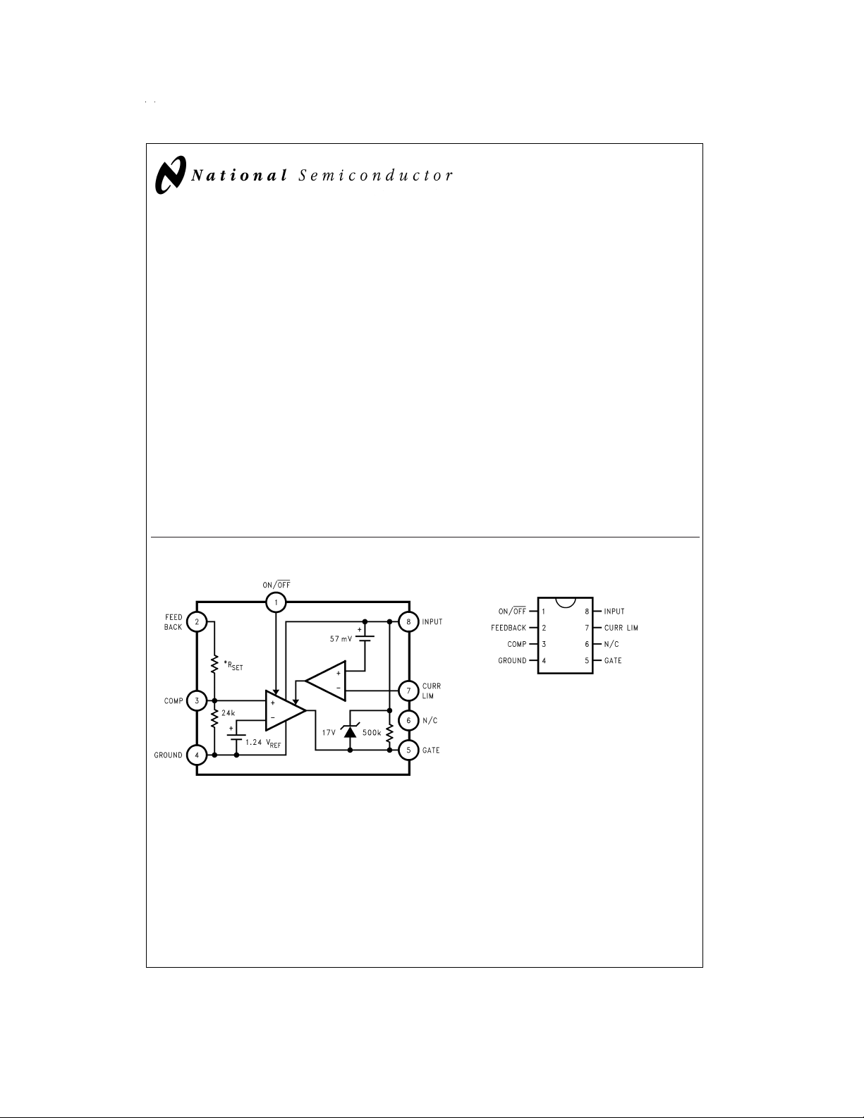
Block Diagram Connection Diagram
Surface Mount Mini SO-8 Package
Top View
For Order Numbers
See
Table 1
See NS Package Number MUA08A
of this Document
@
VIN= 5V)
DS100034-2
*R
values are: 208k for 12V part, 72.8k for 5V part, and 39.9k for 3.3V
SET
part.
© 1999 National Semiconductor Corporation DS100034 www.national.com
DS100034-1
Page 2
Ordering Information
TABLE 1. Package Marking and Ordering Information
Output Voltage Grade Order Information Package Marking Supplied As:
12 A LP2975AIMMX-12 L47A 3.5k Units on Tape and Reel
12 A LP2975AIMM-12 L47A 250 Units on Tape and Reel
12 STD LP2975IMMX-12 L47B 3.5k Units on Tape and Reel
12 STD LP2975IMM-12 L47B 250 Units on Tape and Reel
5.0 A LP2975AIMMX-5.0 L46A 3.5k Units on Tape and Reel
5.0 A LP2975AIMM-5.0 L46A 250 Units on Tape and Reel
5.0 STD LP2975IMMX-5.0 L46B 3.5k Units on Tape and Reel
5.0 STD LP2975IMM-5.0 L46B 250 Units on Tape and Reel
3.3 A LP2975AIMMX-3.3 L45A 3.5k Units on Tape and Reel
3.3 A LP2975AIMM-3.3 L45A 250 Units on Tape and Reel
3.3 STD LP2975IMMX-3.3 L45B 3.5k Units on Tape and Reel
3.3 STD LP2975IMM-3.3 L45B 250 Units on Tape and Reel
www.national.com 2
Page 3
Absolute Maximum Ratings (Note 1)
If Military/Aerospace specified devices are required,
please contact the National Semiconductor Sales Office/
Distributors for availability and specifications.
Storage Temperature Range −65˚C to +150˚C
Operating Junction Temperature
Range −40˚C to +125˚C
Lead Temp. (Soldering, 5 seconds) 260˚C
Input Supply Voltage (Survival) −0.3V to +26V
Input Supply Voltage (Operating) +1.8V to +24V
Current Limit Pins (Survival) −0.3V to +V
Comp Pin (Survival) −0.3V to +2V
Gate Pin (Survival) −0.3V to +V
ON/OFF Pin (Survival) −0.3V to +20V
Feedback Pin (Survival) −0.3V to +24V
ESD Rating 2 kV
Power Dissipation
(Note 2) Internally Limited
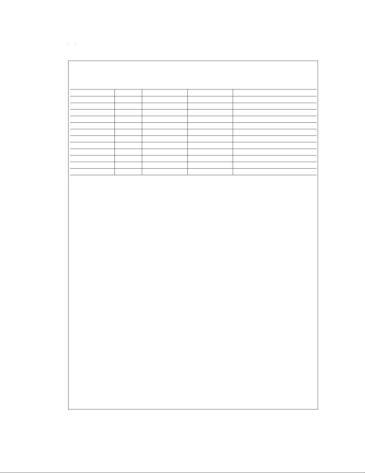
Electrical Characteristics
Limits in standard typeface are for TJ= 25˚C, and limits in boldface type apply over the full operating temperature range. Unless otherwise specified; V
Symbol Parameter Conditions Typ
V
REG
Regulation Voltage
(12V Versions)
Regulation Voltage
(5V Versions)
Regulation Voltage
(3.3V Versions)
V
COMP
I
Q
V
CL
V
ON/OFF
I
ON/OFF
I
G
Comp Pin Voltage V
Quiescent Current VIN= 5V 180 240 240
Current Limit
Sense Voltage
ON/OFF Threshold Output = ON
ON/OFF
Input Bias Current
Gate Drive Current (Sourcing) VG= 7.5V
Gate Drive Current (Sinking) V
V
R(V
G(MIN)
IN
Gate Clamp Voltage VIN= 24V
-G) Resistance from
Gate to V
IN
Open Loop
Voltage Gain
= 1.5V, VIN= 15V.
ON/OFF
LM2975AI-X.X
(Note 3)
LM2975I-X.X
(Note 3)
Min Max Min Max
IN
- 0.5V)>V
IN
(VIN- 5V)
<
<
V
IN
- 0.5V)>V
IN
(VIN- 4.5V)
<
<
V
IN
- 0.5V)>V
IN
(VIN- 3.3V)
<
V
IN
<
24V 12.0 11.820 12.180 11.700 12.300
GATE
11.640 12.360 11.520 12.480
24V 5.0 4.925 5.075 4.875 5.125
GATE
4.850 5.150 4.800 5.200
24V 3.3 3.250 3.350 3.217 3.383
GATE
<
24V 1.240 1.215 1.265 1.203 1.277
3.201 3.399 3.168 3.432
12.5<V
(V
>
5.5
(V
>
3.8
(V
>
REG
1.209 1.271 1.196 1.284
V
= 0V 0.01 11
ON/OFF
VIN= 15V
=0.9XV
V
FB
Output = OFF
V
= 1.5V
ON/OFF
REG
57 45 69 45 69
39 72 39 72
0.94
0.87
1.10 1.10
1.20 1.20
34
0.70 0.70
0.40 0.40
50 50 µA
75 75
3.5 1.3 1.3
=1.1XV
V
V
FB
G
FB
= 7.5V
=0.9XV
REG
REG
0.3 0.3
1100 350 350
40 40
17 15 19 15 19 V
=0.9XV
V
FB
VIN= 24V
V
ON/OFF
VIN= 15V
0.5V ≤ V
=0
GATE
REG
500 kΩ
5000 V/V
≤ 13
IN
IN
Units
V
V
µA320 320
mV
V
mA
µA
Note 1: Absolute maximum ratings indicate limits beyond which damage to the component may occur. Electrical specifications do not apply when operating the device outside of its rated operating conditions.
Note 2: The LP2975 has internal thermal shutdown which activates at a die temperature of about 150˚C. It should be noted that the power dissipated within the
LP2975 is low enough that this protection circuit should never activate due to self-heating, even at elevated ambient temperatures.
www.national.com3
Page 4
Electrical Characteristics (Continued)
Note 3: Limits are 100%production tested at 25˚C. Limits over the operating temperature range are guaranteed through correlation using Statistical Quality Control
(SQC) methods. The limits are used to calculate National’s Average Outgoing Quality Level (AOQL).
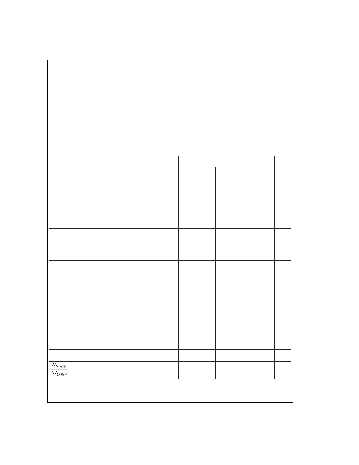
Typical Application Circuits
5V - 3.3V@5A LDO Regulator
*See Application Hints.
**If current limiting is not required, short out this resistor.
*See Application Hints.
***If current limiting is not required, short out this resistor.
DS100034-3
Adjustable Voltage 5A LDO Regulator
DS100034-4
www.national.com 4
Page 5
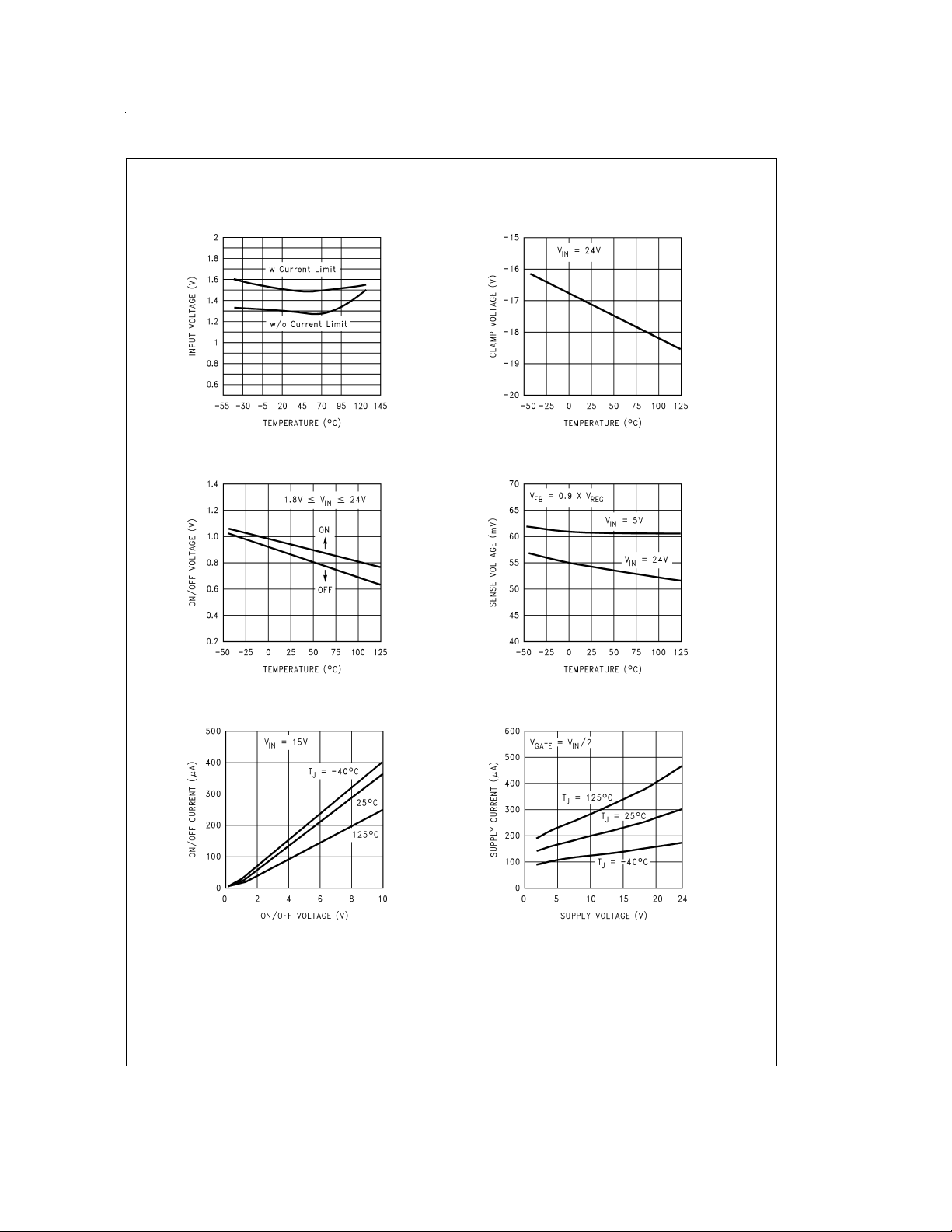
Typical Performance Characteristics Unless otherwise specified: T
is tied to 1.5V.
= 25˚C, CIN= 1 µF, ON/OFF pin
A
Minimum Operating Voltage
ON/OFF Threshold
DS100034-5
VINReferred Gate Clamp Voltage
DS100034-6
Current Limit Sense Voltage
ON/OFF Pin Current
DS100034-7
DS100034-9
DS100034-8
Supply Current
DS100034-10
www.national.com5
Page 6
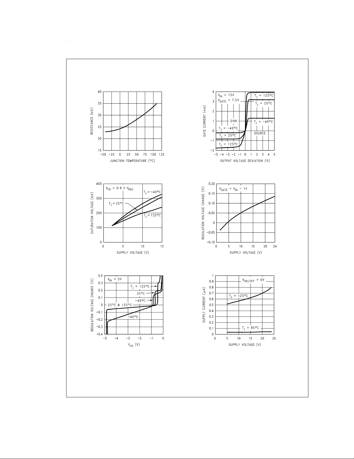
Typical Performance Characteristics Unless otherwise specified: T
is tied to 1.5V. (Continued)
= 25˚C, CIN= 1 µF, ON/OFF pin
A
ON/OFF Input Resistance
Gate-Ground Saturation
DS100034-11
Gate Current
DS100034-34
Line Regulation
DS100034-13
Load Regulation
DS100034-15
www.national.com 6
DS100034-14
Leakage Current
DS100034-35
Page 7

Typical Performance Characteristics Unless otherwise specified: T
is tied to 1.5V. (Continued)
Controller Gain and Phase Response
DS100034-36
Reference Designs
The LP2975 controller can be used with virtually any
P-channel MOSFET to build a wide variety of linear voltage
regulators.
Since it would be impossible to document all the different
voltage and current combinations that could be built, a number of reference designs will be presented along with performance data for each.
THE PERFORMANCE DATA SHOWN IS ACTUAL TEST
DATA, BUT IS NOT GUARANTEED.
#
DESIGN
Circuits)
COMPONENTS:
C
C
C
R
P-FET = NDP6020P
Heatsink: (assuming V
against a
θ
S-A
circuit survivability is not needed, a heatsink with θ
6 ˚C/W is adequate.
PERFORMANCE DATA:
Dropout Voltage
Dropout voltage
differential voltage required by the regulator to keep the output in regulation. It is measured by reducing V
put voltage drops below the nominal value (the nominal
value is the output voltage measured with V
5A for this test.
Load Regulation
Load regulation
voltage as the load current is varied. It is measured by
changing the load resistance and recording the minimum/
1: V
=5V@5A (Refer to Typical Application
OUT
= 82 µF Aluminum Electrolytic
IN
= 120 µF Aluminum Electrolytic
OUT
= 220 pF
F
=10mΩ
SC
≤ 7V and TA≤ 60˚C) if protection
continuous
IN
short-circuit is required, a heatsink with
≤ 1.5 ˚C/W must be used. However, if continuous short-
is defined as the minumum input-to-output
until the out-
IN
= 5.5V). IL=
IN
DROPOUT VOLTAGE = 323 mV
is defined as the maximum change in output
S-A
maximum output voltage. The measured change in output
voltage is divided by the nominal output voltage and expressed as a percentage. V
5mA≤I
≤5A: LOAD REGULATION = 0.012
L
≤ 5A: LOAD REGULATION = 0.135
0 ≤ I
L
Line Regulation
Line regulation
is defined as the maximum change in output
voltage as the input voltage is varied. It is measured by
changing the input voltage and recording the minimum/
maximum output voltage. The measured change in output
voltage is divided by the nominal output voltage and expressed as a percentage. I
5.4V ≤ V
≤ 10V: LINE REGULATION = 0.03
IN
Output Noise Voltage
Output noise voltage was measured by connecting a wideband AC voltmeter (HP 400E) directly across the output capacitor. V
= 6V and IL= 5A for this test.
IN
NOISE = 75 µV (rms)
Transient Response
Transient response
is defined as the change in output voltage which occurs after the load current is suddenly changed.
V
≤
= 5.6V for this test.
IN
The load resistor is connected to the regulator output using a
switch so that the load current increases from 0 to 5A
abruptly.The change in output voltage is shown in the scope
photo below (the vertical scale is 200 mV/division and the
horizontal scale is 10 µs/division). The regulator nominal output (5V) is located on the center line of the photo.
The output shows a maximum change of about −600 mV
compared to nominal. This is due to the relatively small output capacitor chosen for this design. Increasing C
improves transient response (see Designs
= 25˚C, CIN= 1 µF, ON/OFF pin
A
= 5.6V for this test.
IN
%
%
= 5A for this test.
L
%
greatly
OUT
#
2 and#3).
www.national.com7
Page 8

Reference Designs (Continued)
DS100034-37
Transient Response for 0–5A Load Step
#
2: V
DESIGN
Application Circuits, Adjustable Voltage Regulator)
COMPONENTS:
C
= 68 µF Tantalum
IN
=2X68µFTantalum
C
OUT
= 470 pF
C
C
R1 = 237 kΩ,1
R2 = NOT USED
= 0.1Ω
R
SC
Tie feedback pin to V
P-FET = NDT452P
Heatsink: Tab of N-FET is soldered down to 0.6 in
area on PC board.
Output Voltage Adjustment: For this application, a 3.3V part
is “trimmed” down to 3V by using a single external 237 kΩ resistor at R1, which parallels the internal 39.9 kΩ resistor (reducing the effective resistance to 34.2 kΩ).
Because the tempco of the external resistor will not match
the tempco of the internal resistor (which is typically 3000
ppm), this method of adjusting V
tor is only recommended in cases where the output voltage
is adjusted ≤ 10%away from the nominal value.
PERFORMANCE DATA:
Dropout Voltage
Dropout voltage
differential voltage required by the regulator to keep the output in regulation. It is measured by reducing V
put voltage drops below the nominal value (the nominal
value is the output voltage measured with V
0.5A for this test.
Load Regulation
Load regulation
voltage as the load current is varied. It is measured by
changing the load resistance and recording the minimum/
www.national.com 8
=3V@0.5A (Refer to Typical
OUT
%
OUT
2
by using a single resis-
OUT
is defined as the minimum input-to-output
until the out-
IN
= 5V). IL=
IN
DROPOUT VOLTAGE = 141 mV
is defined as the maximum change in output
copper
maximum output voltage. The measured change in output
voltage is divided by the nominal output voltage and expressed as a percentage. V
≤ 0.5A: LOAD REGULATION = 0.034
0 ≤ I
L
= 3.5V for this test.
IN
%
Line Regulation
Line regulation
is defined as the maximum change in output
voltage as the input voltage is varied. It is measured by
changing the input voltage and recording the minimum/
maximum output voltage. The measured change in output
voltage is divided by the nominal output voltage and expressed as a percentage. I
3.5V ≤ V
≤ 6V: LINE REGULATION = 0.017
IN
= 0.5A for this test.
L
%
Output Noise Voltage
Output noise voltage
was measured by connecting a wideband AC voltmeter (HP 400E) directly across the output capacitor. V
= 5V and IL= 0.5A for this test.
IN
NOISE = 85 µV (rms)
Transient Response
Transient response
is defined as the change in output voltage which occurs after the load current is suddenly changed.
V
= 3.5V for this test.
IN
The load resistor is connected to the regulator output using a
switch so that the load current increases from 0 to 0.5A
abruptly.The change in output voltage is shown in the scope
photo (the vertical scale is 20 mV/division and the horizontal
scale is 50 µs/division). The regulator nominal output (3V) is
located on the center line of the photo. A maximum change
of about −50 mV is shown.
DS100034-38
Transient Response for 0–0.5A Load Step
Minimizing C
It is often desirable to decrease the value of C
cost and reduce size. The design guidelines suggest selecting C
put Capacitor
OUT
to set the first pole ≤ 200 Hz (see later section
OUT
), but this is not an absolute requirement in all
OUT
to save
Out-
cases.
The effect of reducing C
phase margin is decreased, the output ringing will increase
when a load step is applied to the output. Eventually, if C
is made small enough, the regulator will oscillate.
To demonstrate these effects, the value of C
#
design
2 is halved by removing one of the two 68 µF output
is to decrease phase margin. As
OUT
in reference
OUT
OUT
capacitors and the transient response test is repeated (see
Page 9

Reference Designs (Continued)
photo below). The total overshoot increases from −50 mV to
about −75 mV, and the second “ring” on the transient is noticeably larger.
DS100034-39
Transient Response with Output Capacitor Halved
The design is next tested with only a 4.7 µF output capacitor
(see scope photo below). Observe that the vertical scale has
been increased to 100 mV/division to accommodate the
−250 mV undershoot. More important is the severe ringing
as the transient decays. Most designers would recognize
this immediately as the warning sign of a marginally stable
design.
DS100034-40
Transient Response with Only 4.7 µF Output Cap
The reason this design is marginally stable is that the 4.7 µF
output capacitor (along with the 6Ω output load) sets the pole
at 5 kHz. Analysis shows that the unity-gain frequency of
f
p
the loop is increased to about 100 kHz, allowing the FET’s
gate capacitance pole f
fore the loop gain goes below unity. Also, because of the low
output voltage, the feedforward capacitor provides less than
10˚ of positive phase shift. For good stability, the output
capcitor needs to be larger than 4.7 µF.
For detailed information on stability and phase margin, see
the
Application Hints
to cause significant phase shift be-
pg
section.
#
DESIGN
Application Circuits, Adjustable Voltage Regulator)
3: V
= 1.5V@6A. (Refer to Typical
OUT
COMPONENTS:
C
= 1000 µF Aluminum Electrolytic
IN
= 4 X 330 µF OSCON Aluminum Electrolytic
C
OUT
= NOT USED
C
C
R1 = 261Ω,1
R2 = 1.21 kΩ,1
R
SC
%
%
=6mΩ
P-FET = NDP6020P
Heatsink: (Assuming V
against a
continuous
<
θ
2.5 ˚C/W must be used. However,if continuous short-
S-A
circuit survivability is not needed, a heatsink with θ
7 ˚C/W is adequate.
≤ 3.3V and TA≤ 60˚C) if protection
IN
short-circuit is required, a heatsink with
S-A
PERFORMANCE DATA:
Dropout Voltage
Dropout voltage
is defined as the minimum input-to-output
differential voltage required by the regulator to keep the output in regulation. It is measured by reducing V
put voltage drops below the nominal value (the nominal
value is the output voltage measured with V
6A for this test.
until the out-
IN
= 3.3V). IL=
IN
DROPOUT VOLTAGE = 0.68V
Load Regulation
Load regulation
is defined as the maximum change in output
voltage as the load current is varied. It is measured by
changing the load resistance and recording the minimum/
maximum output voltage. The measured change in output
voltage is divided by the nominal output voltage and expressed as a percentage. V
≤ 6A: LOAD REGULATION = 0.092
0 ≤ I
L
= 3.3V for this test.
IN
%
Line Regulation
Line regulation
is defined as the maximum change in output
voltage as the input voltage is varied. It is measured by
changing the input voltage and recording the minimum/
maximum output voltage. The measured change in output
voltage is divided by the nominal output voltage and expressed as a percentage. I
3.3V ≤ V
≤ 5V: LINE REGULATION = 0.033
IN
= 6A for this test.
L
%
Output Noise Voltage
Output noise voltage was measured by connecting a wideband AC voltmeter (HP 400E) directly across the output capacitor. V
= 3.3V and IL= 6A for this test.
IN
NOISE = 60 µV (rms)
Transient Response
Transient response
is defined as the change in output voltage which occurs after the load current is suddenly changed.
V
= 3.3V for this test.
IN
The load resistor is connected to the regulator output using a
switch so that the load current increases from 0 to 6A
abruptly.The change in output voltage is shown in the scope
photo (the vertical scale is 50 mV/division and the horizontal
scale is 20 µs/division. The regulator nominal output (1.5V)
is located on the center line of the photo. A maximum change
of about −80 mV is shown.
<
www.national.com9
Page 10

Reference Designs (Continued)
DS100034-41
Transient Response for 0–6A Load Step
Application Hints
SELECTING THE FET
The best choice of FET for a specific application will depend
on a number of factors:
VOLTAGE RATING: The FET must have a Drain-to-Source
breakdown voltage (sometimes called BV
greater than the input voltage.
DRAIN CURRENT: On-state Drain current must be specified
to be greater than the worst-case (short circuit) load current
for the application.
TURN-ON THRESHOLD: The Gate-to-Source voltage
where the FET turns on (called the Gate Threshold Voltage)
is very important. Many FET’s are intended for use with
G-to-S voltages in the 5V to 10V range. These should only
be used in applications where the input voltage is high
enough to provide
>
5V of drive to the Gate.
Newer FET’s are becoming available with lower turn-on
thresholds (Logic-Level FET’s) which turn on fully with a gate
voltage of only 3V to 4V. Low threshold FET’s should be
used in applications where the input voltage is ≤ 5V.
ON RESISTANCE: FET on resistance (often called R
is a critical parameter since it directly determines the minimum input-to-output voltage required for operation at a given
load current (also called dropout voltage).
R
ON is highly dependent on the amount of Gate-to-
DS
Source voltage applied. For example, the R
with V
V
dent, increasing at higher temperatures.
= 5V will typically decrease by about 25%as the
G-S
is increased to 10V. RDSON is also temperature depen-
G-S
The dropout voltage of any LDO design is directly related to
R
ON, as given by:
DS
Where R
Application Circuit).
V
DROPOUT=ILOAD
is the short-circuit current limit set resistor (see
SC
x(RDSON+RSC)
GATECAPACITANCE: Selecting a FET with the lowest possible Gate capacitance improves LDO performance in two
ways:
1) The
Gate
pin of the LP2975 (which drives the Gate of the
FET) has a limited amount of current to source or sink. This
) which is
DSS
ON of a FET
DS
ON)
DS
means faster changes in Gate voltage (which corresponds to
faster transient response) will occur with a smaller amount of
Gate capacitance.
2) The Gate capacitance forms a pole in the loop gain which
can reduce phase margin. When possible, this pole should
be kept at a higher frequency than the cross-over frequency
of the regulator loop (see later section
QUENCY AND PHASE MARGIN
CROSS-OVER FRE-
).
A high value of Gate capacitance may require that a feedforward capacitor be used to cancel some of the excess phase
shift (see later section
FEED-FORWARD CAPACITOR
)to
prevent loop instability.
POWER DISSIPATION: The maximum power dissipated in
the FET in any application can be calculated from:
P
=(VIN−V
Where the term I
should be noted that if the regulator is to be designed to with-
MAX
is the maximum output current. It
MAX
OUT
)xI
MAX
stand short-circuit, a current sense resistor must be used to
limit I
CURRENT LIMITING
to a safe value (refer to section
MAX
).
SHORT-CIRCUIT
The power dissipated in the FET determines the best choice
for package type. A TO-220 package device is best suited for
applications where power dissipation is less than 15W.
Power levels above 15W would almost certainly require a
TO-3 type device.
In low power applications, surface-mount package devices
are size-efficient and cost-effective, but care must be taken
to not exceed their power dissipation limits.
POWER DISSIPATION AND HEATSINKING
Since the LP2975 controller is suitable for use with almost
any external P-FET, it follows that designs can be built which
have very high power dissipation in the pass FET. Since the
controller can not protect the FET from overtemperature
damage, thermal design must be carefully done to assure a
reliable design.
THERMAL DESIGN METHOD: The temperature of the FET
and the power dissipated is defined by the equation:
T
J
=(θ
J-AxPD
)+T
A
Where:
is the junction temperature of the FET.
T
J
is the ambient temperature.
T
A
is the power dissipated by the FET.
P
D
is the junction-to-ambient thermal resistance.
θ
J-A
To ensure a reliable design, the following guidelines are recommended:
1) Design for a maximum (worst-case) FET junction temperature which does not exceed 150˚C.
2) Heatsinking should be designed for worst-case (maximum) values of T
and PD.
A
3) In designs which must survive a short circuit on the output,
the maximum power dissipation must be calculated assuming that the output is shorted to ground:
P
(MAX) = VINxI
D
SC
Where ISCis the short-circuit output current.
4) If the design is not intended to be short-circuit proof, the
maximum power dissipation for intended operation will be:
P
Where I
is the maximum output current.
MAX
LOW POWER (
(MAX) = (VIN−V
D
<
2W) APPLICATIONS: In most cases,
OUT
)xI
MAX
some type of small surface-mount device will be used for the
www.national.com 10
Page 11

Application Hints (Continued)
FET in low power designs. Because of the increased cell
density (and tiny packages) used by modern FET’s, the current carrying capability may easily exceed the power dissipation limits of the package. It is possible to parallel two or
more FET’s, which divides the power dissipation among all
of the packages.
It should be noted that the “heatsink” for a surface mount
package is the copper of the PC board and the package itself
(direct radiation).
Surface-mount devices have the value of θ
typical PC board mounting on their data sheet. In most cases
it is best to start with the known data for the application (P
T
) and calculate the required value of θ
A,TJ
value will define the type of FET and, possibly, the heatsink
required for cooling.
θ
=(TJ−TA)/PD(MAX)
DESIGN EXAMPLE:
and V
OUT
Based on these conditions, power dissipation in the FET dur-
J-A
A design is to be done with VIN=5V
= 3.3V with a maximum load current of 300 mA.
ing normal operation would be:
P
=(VIN−V
D
OUT
)xI
Solving, we find that PD= 0.51W. Assuming that the maximum allowable value of T
70˚C, the value of θ
is 150˚C and the maximum TAis
J
is found to be
J-A
However, if this design must survive a continuous short on
the output, the power dissipated in the FET is higher:
P
(SC) = VINxISC= 5 x 0.33 = 1.65W
D
(This assumes the current sense resistor is selected for an
I
value that is 10%higher than the required 0.3A).
SC
The value of θ
is calculated to be
required to survive continuous short circuit
J-A
49˚C/W.
Having solved for the value(s) of θ
lected. It should be noted that a FET must be used with a
θ
value
J-A
less than or equal to the calculated value.
HIGH POWER (≥2W) APPLICATIONS: As power dissipation increases above 2W, a FET in a larger package must be
used to obtain lower values of θ
rived in the previous section are used to calculate P
θ
.
J-A
Having found θ
value of θ
that a heatsink can be selected:
, it becomes necessary to calculate the
J-A
(the heatsink-to-ambient thermal resistance) so
S-A
θ
= θ
S-A
J-A
. The same formulae de-
J-A
−(θ
+ θ
J-C
Where:
is the junction-to-case thermal resistance. This pa-
θ
J-C
rameter is the measure of thermal resistance between the
semiconductor die inside the FET and the surface of the
case of the FET where it mounts to the heatsink (the value of
θ
can be found on the data sheet for the FET). A typical
J-C
FET in a TO-220 package will have a θ
mately 2–4˚C/W, while a device in a TO-3 package will be
about 0.5–2˚C/W.
θ
is the case-to-heatsink thermal resistance, which
C-S
measures how much thermal resistance exists between the
surface of the FET and the heatsink. θ
the package type and mounting method. A TO-220 package
with mica insulator and thermal grease secured to a heatsink
will have a θ
package mounted in the same manner will have a θ
value in the range of 1–1.5˚C/W. A TO-3
C-S
specified for a
J-A
needed. This
J-A
LOAD
157˚C/W.
, a FET can be se-
J-A
)
C-S
value of approxi-
J-C
is dependent on
C-S
C-S
and
D
value
of 0.3–0.5˚C/W. The best source of information for this is
heatsink catalogs (Wakefield, AAVID, Thermalloy) since they
also sell mounting hardware.
θ
is the heatsink-to-ambient thermal resistance, which
S-A
defines how well a heatsink transfers heat into the air. Once
this is determined, a heatsink must be selected which has a
value which is less than or equal to the computed value. The
value of θ
sheet for a heatsink, but the information is sometimes given
is usually listed in the manufacturer’s data
S-A
in a graph of temperature rise vs. dissipated power.
DESIGN EXAMPLE:
A design is to be done which takes
3.3V in and provides 2.5V out at a load current of 7A. The
power dissipation will be calculated for both normal opera-
,
D
tion and short circuit conditions.
For normal operation:
P
=(VIN−V
D
OUT
)xI
LOAD
= 5.6W
If the output is shorted to ground:
(SC) = VINxISC= 3.3 x 7.7 = 25.4W
P
D
(Assuming that a sense resistor is selected to set the value
of I
10%above the nominal 7A).
SC
will be calculated assuming a maximum TAof 70˚C and
θ
J-A
a maximum T
of 150˚C:
J
=(TJ−TA)/PD(MAX)
θ
J-A
For normal operation:
= (150 − 70) / 5.6 = 14.3˚C/W
θ
J-A
For designs which must operate with the output shorted to
ground:
θ
= (150 − 70) / 25.4 = 3.2˚C/W
J-A
The value of 14.3˚C/W can be easily met using a TO-220 device. Calculating the value of θ
value of θ
= 3˚C/W and θ
J-C
= θ
θ
S-A
J-A
=14.3−(3+1)=10.3˚C/W
θ
S-A
required (assuming a
S-A
= 1˚C/W):
C-S
−(θ
+ θ
J-C
)
C-S
Any heatsink may be used with a thermal resistance ≤
10.3˚C/W
@
5.6W power dissipation (refer to manufacturer’s
data sheet curves). Examples of suitable heatsinks are Thermalloy #6100B and IERC #LATO127B5CB.
However, if the design must survive a sustained short on the
output, the calculated θ
possibility of using a TO-220 package device.
Assuming a TO-3 device is selected with a θ
1.5˚C/W and θ
value of θ
C-S
:
S-A
θ
= 3.2 − (1.5 + 0.4) = 1.3˚C/W
θ
S-A
value ≤1.3˚C/W would require a relatively large heat-
A θ
S-A
sink, or possibly some kind of forced airflow for cooling.
value of 3.2˚C/W eliminates the
J-A
value of
= 0.4˚C/W, we can calculate the required
= θ
−(θ
S-A
J-A
+ θ
J-C
J-C
)
C-S
SHORT-CIRCUIT CURRENT LIMITING
Short-circuit current limiting is easiliy implemented using a
single external resistor (R
culated from:
). The value of RSCcan be cal-
SC
R
SC=VCL/ISC
Where:
is the desired short circuit current.
I
SC
is the current limit sense voltage.
V
CL
The value of V
listed in the Electrical Characteristics section. When doing a
is 57 mV (typical), with guaranteed limits
CL
worst-case calculation for power dissipation in the FET, it is
important to consider both the tolerance of V
ance (and temperature drift) of R
.
SC
and the toler-
CL
www.national.com11
Page 12

Application Hints (Continued)
For maximum accuracy, the
pins must be Kelvin connected to RSC, to avoid errors
caused by voltage drops along the traces carrying the current from the input supply to the
EXTERNAL CAPACITORS
The best capacitors for use in a specific design will depend
on voltage and load current (examples of tested circuits for
several different output voltages and currents are provided in
a previous section.)
Information in the next sections is provided to aid the designer in the selection of the external capacitors.
INPUT CAPACITOR: Although not always required, an input
capacitor is recommended. Good bypassing on the input assures that the regulator is working from a source with a low
impedance, which improves stability. A good input capacitor
can also improve transient response by providing a reservoir
of stored energy that the regulator can utilize in cases where
the load current demand suddenly increases. The value
used for C
erence Designs section for examples of input capacitors.
may be increased without limit. Refer to the Ref-
IN
OUTPUT CAPACITOR: The output capacitor is required for
loop stability (compensation) as well as transient response.
During sudden changes in load current demand, the output
capacitor must source or sink current during the time it takes
the control loop of the LP2975 to adjust the gate drive to the
pass FET.As a general rule, a larger output capacitor will improve both transient response and phase margin (stability).
The value of C
may be increased without limit.
OUT
OUTPUT CAPACITOR AND COMPENSATION:
pensation for the LP2975 is derived from C
cases, the feed-forward capacitor C
forms a pole (referred to as fp) in conjuction with the
C
OUT
load resistance which causes the loop gain to roll off (decrease) at an additional −20 dB/decade. The frequency of
the pole is:
f
=0.16/[(RL+ESR)xC
p
Where:
is the load resistance.
R
L
is the value of the output capacitor.
C
OUT
ESR is the equivalent series resistance of C
As a general guideline, the frequency of f
Hz. It should be noted that higher load currents correspond
to lower values of R
to keep f
p
L
at a given frequency.
DESIGN EXAMPLE:
capacitance for a design whose output specifications are 5V
@
1A:
=0.16/[(RL+ESR)xC
f
p
Re-written:
=0.16/[fpx(RL+ ESR) ]
C
OUT
Values used for the calculation:
= 200 Hz, RL=5Ω, ESR = 0.1Ω (assumed).
f
p
Solving for C
would be 180 µF).
OUT
,weget
The ESR of the output capacitor is very important for stability,as it creates a zero (f
shift resulting from one of the poles present in the loop. The
frequency of the zero is calculated from:
f
= 0.16 / (ESR x C
z
www.national.com 12
INPUT
and
CURRENT LIMIT
Source
pin of the FET.
Loop com-
and, in some
OUT
(see next section).
F
]
OUT
.
OUT
should be ≤ 200
p
, which requires that C
be increased
OUT
Select the minimum required output
]
OUT
157 µF
(nearest standard size
) which cancels much of the phase
z
)
OUT
For best results in most designs, the frequency of f
fall between 5 kHz and 50 kHz. It must be noted that the values of C
verely in the case of aluminum electrolytics), and this must
and ESR usually vary with temperature (se-
OUT
should
z
be taken into consideration.
For the design example (V
which meets the f
ESR yields:
requirements. Solving the equation for
z
ESR = 0.16 / (f
Assuming f
for the 180 µF capacitor are found to be:
= 5 kHz and 50 kHz, the limiting values of ESR
z
=5V@1A), select a capacitor
OUT
)
zxCOUT
18 mΩ≤ESR ≤ 0.18Ω
A good-quality, low-ESR capacitor type such as the Panasonic HFQ is a good choice. However, the 10V/180 µF capacitor (#ECA-1AFQ181) has an ESR of 0.3Ω which is not in
the desired range.
To assure a stable design, some of the options are:
1) Use a different type capacitor which has a lower ESR
such as an organic-electrolyte OSCON.
2) Use a higher voltage capacitor. Since ESR is inversely
proportional to the physical size of the capacitor, a higher
voltage capacitor with the same C value will typically have a
lower ESR (because of the larger case size). In this example, a Panasonic ECA-1EFQ181 (which is a 180 µF/25V
part) has an ESR of 0.17Ω and would meet the desired ESR
range.
3) Use a feed-forward capacitor (see next section).
FEED-FORWARD CAPACITOR: Although not required in
every application, the use of a feed-forward capacitor (C
can yield improvements in both phase margin and transient
response in most designs.
The added phase margin provided by C
lations in cases where the required value of C
can not be easily obtained (see previous section).
C
can also reduce the phase shift due to the pole resulting
F
from the Gate capacitance, stabilizing applications where
can prevent oscil-
F
OUT
and ESR
this pole occurs at a low frequency (before cross-over) which
would cause oscillations if left uncompensated (see later
section
GATE CAPACITANCE POLE FREQUENCY).
Even in a stable design, adding CFwill typically provide more
optimal loop response (faster settling time). For these reasons,
the use of a feed-forward capacitor is always rec-
ommended.
CFis connected across the top resistor in the divider used to
set the output voltage (see Typical Application Circuit). This
forms a zero in the loop response (defined as f
quency is:
f
=6.6x10⁻⁶/[CFx(V
zf
When solved for C
C
, the fzfequation is:
F
=6.6x10⁻⁶/[fzfx(V
F
For most applications, f
50 kHz.
zf
OUT
OUT
should be set between 5 kHz and
), whose fre-
zf
/1.24−1)]
/1.24−1)]
ADJUSTING THE OUTPUT VOLTAGE
If an output voltage is required which is not available as a
standard voltage, the LP2975 can be used as an adjustable
regulator (see Typical Application circuit). The external resistors R1 and R2 (along with the internal 24 kΩ resistor) set
the output voltage.
It is important to note that R2 is connected in parallel with the
internal 24 kΩ resistor. If we define R
tance between the COMP pin and ground, then its value
as the total resis-
EQ
will be the parallel combination of R2 and 24 kΩ:
)
F
Page 13

Application Hints (Continued)
R
= (R2 x 24k) / (R2 + 24k)
It follows that the output voltage will be:
Some important considerations for an adjustable design:
The tolerance of the internal 24 kΩ resistor is about
Also, its temperature coefficient is almost certainly different
than the TC of the external resistor that is used for R2.
For these reasons, it is recommended that R2 be set at a
value that is not greater than 1.2k. In this way, the value of
R2 will dominate R
nal 24k resistor will have a negligible effect on output voltage
accuracy.
To determine the value for R1:
External Capacitors (Adjustable Application)
All information in the previous section
TORS
tion of how to select the value of the feed-forward capacitor.
The feed-forward capacitor C
(see Typical Application Circuit) performs exactly the same
function as described in the previous section
WARD CAPACITOR.
selected, a different formula must be used to determine the
value of C
As stated previously, the optimal frequency at which to place
the zero f
OPTIMIZING DESIGN STABILITY
Because the LP2975 can be used with a variety of different
applications, there is no single set of components that are
best suited to every design. This section provides information which will enable the designer to select components that
optimize stability (phase margin) for a specific application.
Gate Capacitance
An important consideration of a design is to identify the frequency of the pole which results from the capacitance of the
Gate of the FET (this pole will be referred to as f
gets closer to the loop crossover frequency, the phase margin is reduced. Information will now be provided to allow the
total Gate capacitance to be calculated so that f
proximated.
The first step in calculating fp is to determine how much ef-
fective Gate capacitance (C
calculating C
Where:
is the Gate-to-Source capacitance, which is found
C
GS
from the values (refer to FET data sheet for values of C
and C
RSS
GGDis the Gate-to-Drain capacitance, which is equal to:
Gmis the transconductance of the FET. The FET data
sheet specifies forward transconductance (G
value of drain current (defined as I
sired value of load current (defined as I
EQ
=1.24[(R1/REQ)+1]
V
OUT
±
20%.
, and the tolerance and TC of the inter-
EQ
R1=R
[(V
OUT
/ 1.24) − 1]
EQ
EXTERNAL CAPACI-
applies to the adjustable application with the excep-
in the adjustable application
C
FEEDFOR-
However, because R1 is user-
:
C
is usually between 5 kHz and 50 kHz.
zf
C
EFF=CGS+CGD
):
=1/(2πxR1xfzf)
C
C
is:
EFF
C
GS=CISS−CRSS
G
m=Gfs
) is present. The formula for
EFF
[1+Gm(RL/ / ESR) ]
C
GD=CRSS
). To find Gm at the de-
D
L
1/2
x(IL/ID)
). As f
pg
can be ap-
pg
) at some
fs
), use the formula:
ISS
Where:
is the load resistance.
R
L
ESR is the equivalent series resistance of the output ca-
pacitor.
The term R
It can be seen from these equations that C
To get the worst-case (maximum) value for C
maximum value of load current, which also means the minimum value of load resistance R
most cases, the ESR is the dominant term which determines
the value of R
/ / ESR is defined as:
L
xESR)/(RL+ ESR)
(R
L
/ / ESR.
L
varies with RL.
EFF
, use the
EFF
. It should be noted that in
L
Gate Pin Output Impedance
DS100034-20
Gate Capacitance Pole Frequency (f
)
pg
The pole frequency resulting from the Gate capacitance
C
is defined as fpgand can be approximated from:
EFF
≅
0.16 / (ROxC
f
pg
EFF
)
Where:
is the output impedance of the LP2975 Gate pin which
R
O
drives the Gate of the FET. It is important to note that R
a function of input supply voltage (see graph
OUTPUT IMPEDANCE).
R
is about 550Ω@VIN= 24V, increasing to about 1.55 kΩ
O
@
VIN=3V.
pg
Using the equation for f
showing how f
(see graph
pg
fpgvs. C
As shown, the minimum value of
, a family of curves are provided
pg
varies with C
):
EFF
fpgvs. C
for several values of R
EFF
EFF
DS100034-21
O
GATE PIN
is
O
www.national.com13
Page 14

Application Hints (Continued)
As can be seen in the graph, values of C
500 pF–2500 pF range produce values for f
40 kHz and 700 kHz. To determine what effect f
on stability, the bandwidth of the regulator loop must be calculated (see next section
PHASE MARGIN
CROSSOVER FREQUENCY AND
).
Crossover Frequency and Phase Margin
The term f
the regulator loop (which is the frequency where the gain
will be used to define the crossover frequency of
c
curve crosses the 0 dB axis). The importance of this frequency is that it is the point where the loop gain goes below
unity, which marks the usable bandwidth of the regulator
loop.
It is the phase margin (or lack of it) at f
whether the regulator is stable. Phase margin is defined as
c
the total phase shift subtracted from 180˚. In general, a
stable loop requires at least 20˚-30˚ of phase margin at f
can be approximated by the following equation (all terms
f
c
have been previously defined):
DS100034-23
This equation assumes that no C
is used and fpg/f
F
If the frequency of the Gate capacitance pole f
calculated (previous section), the amount of added phase
shift may now be determined. As shown in the graph below
(see graph
added phase shift increases as f
The amount of phase shift due to f
oscillation takes place depends on how much added phase
shift is present as a result of the C
section
PHASE SHIFT DUE TO fpg),
OUTPUT CAPACITOR).
Phase Shift Due to f
approaches fc.
pg
that can occur before
pg
pole (see previous
OUT
pg
DS100034-22
Because of this, there is no exact number for fpg/fcthat can
be given as a fixed limit for stable operation. However, as a
general guideline, it is recommended that f
pg
If this is not found to be true after inital calculations, the ratio
of f
can be increased by either reducing C
pg/fc
a different FET) or using a larger value of C
Along with these two methods, another technique for improv-
ing loop stability is the use of a feed-forward capacitor (see
in the
EFF
between
pg
will have
pg
that determines
c
>
1.
c
has been
pg
the amount of
≥ 3fc.
(selecting
EFF
.
OUT
next section
FEED-FORWARD COMPENSATION).
improve phase margin by cancelling some of the excess
phase shift.
Feed-Forward Compensation
Phase shift in the loop gain of the regulator results from f
(the pole from the output capacitor and load resistance), f
(the pole from the FET gate capacitance), as well as the IC’s
internal controller pole (see typical curve). If the total phase
shift becomes excessive, instability can result.
The total phase shift can be reduced using feed-forward
compensation, which places a zero in the loop to reduce the
effects of the poles.
The feed-forward capacitor C
it is selected to set the zero at the correct frequency. It is im-
can accomplish this, provided
F
portant to point out that the feed-forward capacitor produces
both a zero and a pole
will be defined as f
defined as f
.
are:
f
zf
f
pf
. The frequency where the zero occurs
, and the frequency of the pole will be
zf
. The equations to calculate the frequencies
pf
6.6x10
6.6x10
-6
/[CFx(V
-6
OUT
/[CFx (1 − 1.24/V
=
=
In general, the feed-forward capacitor gives the greatest improvement in phase margin (provides the maximum reduction in phase shift) when the zero occurs at a frequency
where the loop gain is
>
1 (before the crossover frequency).
The pole must occur at a higher frequency (the higher the
better) where most of the phase shift added by the new pole
occurs beyond the crossover frequency. For this reason, the
pole-zero pair created by C
proving loop stability as they get farther apart in frequency.
In reviewing the equations for f
they get closer together in frequency as V
For this reason, the use of C
output voltages, declining as V
(where C
has no effect at all).
F
become more effective at im-
F
and fpf, it can be seen that
zf
gives greatest benefit at higher
F
OUT
In selecting a value of feed-forward capacitor, the crossover
frequency f
quency of the zero (f
range:
must first be calculated. In general, the fre-
c
) set by this capacitor should be in the
zf
0.2 f
≤ fzf≤ 1.0 f
c
The equation to determine the value of the feed-forward capacitor in fixed-voltage applications is:
=
C
F
6.6x10
-6
/[fzfx(V
OUT
In adjustable applications (using an external resistive divider) the capacitor is found using:
=
C
1/(2 π xR1xf
C
SUMMARY OF STABILITY INFORMATION
This section will present an explanation of theory and terminology used to analyze loop stability, along with specific information related to stabilizing LP2975 applications.
BODE PLOTS AND PHASE SHIFT
Loop gain information is most often presented in the form of
a Bode Plot, which plots Gain (in dB) versus Frequency (in
Hertz).
A Bode Plot also conveys phase shift information, which can
be derived from the locations of the poles and zeroes.
POLE: A pole causes the slope of the gain curve to decrease by an additional −20 dB/decade, and it also causes
phase lag (defined as negative phase shift) to occur.
A single pole will cause a maximum −90˚ of phase lag (see
graph
EFFECTS OF A SINGLE POLE
This can
/1.24 − 1) ]
)]
OUT
decreases.
OUT
approaches 1.24V
c
/1.24 − 1) ]
)
zf
). It should be noted
p
pg
www.national.com 14
Page 15

Application Hints (Continued)
that when the total phase shift at 0 dB reaches (or gets close
to) −180˚, oscillations will result. Therefore, it can be seen
that at least two poles in the gain curve are required to
cause instability.
ZERO:A zero has an effect that is exactly
A zero will add a maximum +90˚ of phase lead (defined as
positive phase shift). Also, a zero causes the slope of the
gain curve to increase by an additional +20 dB/decade (see
graph
EFFECTS OF A SINGLE ZERO
Effects of a Single Pole
TOTAL PHASE SHIFT: The actual test of whether or not a
regulator is stable is the amount of phase shift that is present
when the gain curve crosses the 0 dB axis (the frequency
where this occurs was previously defined as f
The phase shift at f
poles and zeroes on the Bode plot and adding up the contri-
can be estimated by looking at all of the
c
butions of phase lag and lead from each one. As shown in
the graphs, most of the phase lag (or lead) contributed by a
pole (or zero) occurs within one decade of the frequency of
the pole (or zero).
In general, a phase margin (defined as the difference between the total phase shift and −180˚) of at least 20˚ to 30˚
is required for a stable loop.
Effects of a Single Zero
opposite to a pole
).
DS100034-25
).
c
STABILITY ANALYSIS OF TYPICAL APPLICATIONS
The first application to be analyzed is a fixed-output voltage
regulator with no feed-forward capacitor (see graph
PLOT WITHOUT FEED-FORWARD
.
Stable Plot without Feed-Forward
In this example, the value of C
pole formed by C
at 200 Hz. The ESR of C
by the ESR and C
selections follow the general guidelines stated previously in
and RL(previously defined as fp)isset
OUT
OUT
(defined as fz) is set at 5 kHz (these
OUT
).
is selected so that the
OUT
is selected so that zero formed
this document). Note that the gate capacitance is assumed
to be moderate, with the pole formed by the C
as f
) occurring at 100 kHz.
pg
To estimate the total phase margin, the individual phase shift
contributions of each pole and zero will be calculated assuming f
=
p
200 Hz, f
z
=
5 kHz, f
=
10 kHz and f
c
Controller pole shift=−90˚
shift=−arctan (10k/200)=−89˚
f
p
shift=arctan (10k/5k)=+63˚
f
z
shift=−arctan (10k/100k)=−6˚
f
pg
Summing the four numbers, the estimate for the total phase
shift is −122˚, which corresponds to a phase margin of 58˚.
This application is stable, but could be improved by using a
feed-forward capacitor (see next section).
EFFECT OF FEED-FORWARD: The example previously
used will be continued with the addition of a feed-forward capacitor C
FEED-FORWARD
fined as f
viously defined as f
corresponds to V
(see graph
F
) is set at 10 kHz and the pole formed by CF(pre-
zf
IMPROVED PHASE MARGIN WITH
). The zero formed by CF(previously de-
) is set at 40 kHz (the 4X ratio of fpf/f
pf
=
5V).
OUT
DS100034-27
GATE
pg
STABLE
(defined
=
100 kHz:
zf
DS100034-26
www.national.com15
Page 16

Application Hints (Continued)
Improved Phase Margin with Feed-Forward
DS100034-28
To estimate the total phase margin, the individual phase shift
contributions of each pole and zero will be calculated assum-
=
200 Hz, f
ing f
p
=
f
50 kHz, and f
c
Controller pole shift=−90˚
shift=−arctan (50k/200)=−90˚
f
p
shift=arctan (50k/5k)=+84˚
f
z
shift=arctan (50k/100k)=+79˚
f
zf
shift=−arctan (50k/40k)=−51˚
f
pf
shift=−arctan (50k/100k)=−27˚
f
pg
Summing the six numbers, the estimate for the total phase
shift is −95˚, which corresponds to a phase margin of 85˚
(a 27˚ improvement over the same application without the
feed-forward capacitor).
For this reason, a feed-forward capacitor is recommended in
all applications. Although not always required, the added
phase margin typically gives faster settling times and provides some design guard band against C
tions with temperature.
CAUSES AND CURES OF OSCILLATIONS
The most common cause of oscillations in an LDO application is the output capacitor ESR. If the ESR is too high or too
low, the zero (f
HIGH ESR: To illustrate the effect of an output capacitor with
high ESR, the previous example will be repeated except that
the ESR will be increased by a factor of 20X. This will cause
the frequency of the zero f
moves it from 5 kHz down to 250 Hz (see graph
UNSTABLE WITHOUT FEED-FORWARD
=
5 kHz, f
z
=
100 kHz:
pg
) does not provide enough phase lead.
z
=
10 kHz, f
zf
to decrease by 20X, which
z
pf
and ESR varia-
OUT
=
HIGH ESR
).
40 kHz,
High ESR Unstable without Feed-Forward
DS100034-29
As shown, moving the location of f
tends the bandwidth, pushing the crossover frequency f
to about 200 kHz. In viewing the plot, it can be seen that f
lower in frequency ex-
z
out
c
and fzessentially cancel out, leaving only the controller pole
and f
. However, since fpgnow occurs well before fc, it will
pg
cause enough phase shift to leave very little phase margin.
This application would either oscillate continuously or be
marginally stable (meaning it would exhibit severe ringing on
transient steps).
This can be improved by adding a feed-forward capacitor C
which adds a zero (f
graph
HIGH ESR CORRECTED WITH FEED-FORWARD
In this case, C
quency as f
to f
frequency, it will add<45˚ of phase lag, leaving a phase
margin of
pg
). Assuming the added pole fpfis near or beyond the f
pg
>
) and a pole (fpf) to the gain plot (see
zf
is selected to place fzfat about the same fre-
F
(essentially cancelling out the phase shift due
45˚ (adequate for good stability).
High ESR Corrected with Feed-Forward
DS100034-31
LOW ESR: To illustrate how an output capacitor with low
ESR can cause an LDO regulator to oscillate, the same example will be shown except that the ESR will be reduced sufficiently to increase the original f
The plot now shows (see graph
WITHOUT FEED-FORWARD
f
has moved down to about 8 kHz. Since fzis 6X fc, it means
c
that the zero f
which is not sufficient for stability.
can only provide about 9˚ of phase lead at fc,
z
from 5 kHz to 50 kHz.
z
LOW ESR UNSTABLE
) that the crossover frequency
p
,
F
).
c
www.national.com 16
Page 17

Application Hints (Continued)
Low ESR Unstable without Feed-Forward
DS100034-30
This application can also be improved by adding a feedforward capacitor. C
the gain plot (see graph
FEED-FORWARD
The crossover frequency f
lected so that f
(which means V
erably improved. Calculating out all the poles and zeroes,
the phase margin is increased from 9˚ to 43˚ (adequate for
good stability).
Low ESR Corrected with Feed-Forward
will add both a zero fzfand pole fpfto
F
LOW ESR CORRECTED WITH
).
is now about 10 kHz. If CFis se-
c
is about 5 kHz, and fpfis about 20 kHz
zf
=
5V), the phase margin will be consid-
OUT
The use of a feed-forward capacitor C
cess phase shift due to f
output voltage (see next section).
, but its effectiveness depends on
pg
LOW OUTPUT VOLTAGE AND C
will help reduce ex-
F
F
The feed-forward capacitor CFwill provide a positive phase
shift (lead) which can be used to cancel some of the excess
phase lag from any of the various poles present in the loop.
However, it is important to note that the effectiveness of C
decreases with output voltage.
This is due to the fact that the frequencies of the zero f
pole f
get closer together as the output voltage is reduced
pf
(see equations in section
TION
).
is more effective when the pole-zero pair are farther
C
F
apart, because there is less self cancellation. The net benefit
in phase shift provided by C
lead (positive phase shift) from f
phase shift) from f
quency f
. As the pole and zero frequency approach each
c
other, that difference diminishes to nothing.
The amount of phase lead at f
both on the f
To illustrate this more clearly, a graph is provided which
ratio and the location of fzwith respect to fc.
zf/fpf
FEED-FORWARD COMPENSA-
is the difference between the
F
and the lag (negative
which is present at the crossover fre-
pf
zf
provided by CFdepends
C
shows how much phase lead can be obtained for V
12V,5V,and 3.3V (see graph
C
).
F
Phase Lead Provided by C
PHASE LEAD PROVIDED BY
F
zf
OUT
and
F
=
DS100034-32
EXCESSIVE GATE CAPACITANCE: Higher values of gate
capacitance shift the pole f
cause stability problems (see previous section
PACITANCE POLE FREQUENCY
fpgvs. C
40 kHz and 500 kHz. How much phase shift this adds de-
, the pole fpgwill likely fall somewhere between
EFF
pends on the crossover frequency f
to lower frequencies, which can
pg
GATE CA-
). As shown in the graph
.
c
The effect of gate capacitance becomes most important at
high values of ESR for the output capacitor (see graph
ESR UNSTABLEWITHOUT FEED-FORWARD
ues of ESR increase f
tive gain portion of the curve. As f
quency (corresponding to higher values of gate
, which brings fpgmore into the posi-
c
moves to a lower fre-
pg
HIGH
). Higher val-
capacitance), this effect becomes even worse.
This points out why FET’s should be selected with the lowest
possible gate capacitance: it makes the design more tolerant
of higher ESR values on the output capacitor.
DS100034-33
The most important information on the graph is the frequency range of f
(most positive phase shift):
OUT
OUT
OUT
=
=
=
For V
For V
For V
which will provide the maximum benefit
zf
<
<
f
12V: 0.1 f
5V: 0.2 f
3.3V: 0.2 f
c
1.0 f
c
z
<
f
z
<
c
c
<
1.2 f
c
<
f
1.3 f
z
c
It’s also important to note how the maximum available phase
shift that C
than 50˚ can be obtained, but at 3.3V less than 30˚ is pos-
can provide drops off with V
F
. At 12V, more
OUT
sible. The lesson from this is that higher voltage designs are
more tolerant of phase shifts from both f
tance pole) and incorrect placement of f
output capacitor ESR is not at its nominal value). At lower
values of V
selected since C
, these parameters must be more precisely
OUT
can not provide as much correction.
F
(the gate capaci-
pg
(which means the
z
GENERAL DESIGN PROCEDURE
Assuming that V
, and RLare defined:
IN,VOUT
www.national.com17
Page 18

Application Hints (Continued)
1) Calculate the required value of capacitance for C
that the pole f
PACITOR
≤ 200 Hz (see previous section
p
). For this calculation, an ESR of about 0.1Ω can
be assumed for the purpose of determining C
IMPORTANT: If a smaller value of output capacitor is used
(so that the value of f
control loop will be reduced. This will result in increased ring-
>
200 Hz), the phase margin of the
p
ing on the output voltage during a load transient. If the output
capacitor is made extremely small, oscillations will result.
To illustrate this effect, scope photos have been presented
showing the output voltage of reference design
output capacitor is reduced to approximately 1/30 of the
nominal value (the value which sets f
the effect of deviating from the nominal value is gradual and
= 200 Hz). As shown,
p
the regulator is quite robust in resisting going into oscillations.
2) Approximate the crossover frequency f
tion in the previous section
AND PHASE MARGIN
CROSSOVER FREQUENCY
.
c
3) Calculate the required ESR of the output capacitor so that
the frequency of the zero f
tion
OUTPUT CAPACITOR
is set to 0.5 fc(see previous sec-
z
).
4) Calculate the value of the feed-forward capacitor C
that the zero f
occurs at the frequency which yields the
zf
OUT
OUTPUT CA-
.
OUT
#
2asthe
using the equa-
F
maximum phase gain for the output voltage selected (see
so
formula for calculating C
FORWARD CAPACITOR
previous section
LOW OUTPUT VOLTAGE AND C
is in the previous section
F
.
). The
F
FEED-
Lower ESR electrolytics are available which use organic
electrolyte (OSCON types), but are more costly than typical
aluminum electrolytics.
If the calculated value of ESR is higher than what is found in
the selected capacitor, an external resistor can be placed in
series with C
OUT
.
LOW VOLTAGE DESIGNS: Designs which have a low output voltage (where the positive effects of C
may be marginally stable if the C
carefully selected.
OUT
are very small)
F
and ESR values are not
Also, if the FET gate capacitance is large (as in the case of
a high-current FET), the pole f
enough in frequency to cause a problem.
could possibly get low
pg
The solution in both cases is to increase the amount of output capacitance which will shift f
reduce overall loop bandwidth). The ESR and C
tions should be repeated, since this changes the crossover
frequency f
.
c
to a lower frequency (and
p
calcula-
F
so
www.national.com 18
Page 19

Physical Dimensions inches (millimeters) unless otherwise noted
LP2975 MOSFET LDO Driver/Controller
Surface Mount Mini SO-8 Package
NS Package Number MUA08A
LIFE SUPPORT POLICY
NATIONAL’S PRODUCTS ARE NOT AUTHORIZED FOR USE AS CRITICAL COMPONENTS IN LIFE SUPPORT
DEVICES OR SYSTEMS WITHOUT THE EXPRESS WRITTEN APPROVAL OF THE PRESIDENT AND GENERAL
COUNSEL OF NATIONAL SEMICONDUCTOR CORPORATION. As used herein:
1. Life support devices or systems are devices or
systems which, (a) are intended for surgical implant
into the body, or (b) support or sustain life, and
whose failure to perform when properly used in
accordance with instructions for use provided in the
2. A critical component is any component of a life
support device or system whose failure to perform
can be reasonably expected to cause the failure of
the life support device or system, or to affect its
safety or effectiveness.
labeling, can be reasonably expected to result in a
significant injury to the user.
National Semiconductor
Corporation
Americas
Tel: 1-800-272-9959
Fax: 1-800-737-7018
Email: support@nsc.com
www.national.com
National does not assume any responsibility for use of any circuitry described, no circuit patent licenses are implied and National reserves the right at any time without notice to change said circuitry and specifications.
National Semiconductor
Europe
Fax: +49 (0) 1 80-530 85 86
Email: europe.support@nsc.com
Deutsch Tel: +49 (0) 1 80-530 85 85
English Tel: +49 (0) 1 80-532 78 32
Français Tel: +49 (0) 1 80-532 93 58
Italiano Tel: +49 (0) 1 80-534 16 80
National Semiconductor
Asia Pacific Customer
Response Group
Tel: 65-2544466
Fax: 65-2504466
Email: sea.support@nsc.com
National Semiconductor
Japan Ltd.
Tel: 81-3-5639-7560
Fax: 81-3-5639-7507
 Loading...