

Datasheet LP2966IMMX-3030, LP2966IMMX-2828, LP2966IMMX-1833, LP2966IMM-5050, LP2966IMM-3636 Datasheet (NSC)
...Page 1
LP2966
Dual 150mA Ultra Low-Dropout Regulator
LP2966 Dual 150mA Ultra Low-Dropout Regulator
April 2000
General Description
The LP2966 dual ultra low-dropout (LDO) regulator operates
from a +2.70V to +7.0V input supply. Each output delivers
150mAoverfulltemperaturerange.The IC operates with extremely low drop-out voltage and quiescent current, which
makes it very suitable for battery powered and portable applications. Each LDO in the LP2966 has independent shutdown capability. The LP2966 provides low noise performance with low ground pin current in an extremely small
MSOP-8 package (refer to package dimensions and connection diagram for more information on MSOP-8 package). A
wide range of preset voltage options are available for each
output. In addition to the voltage combinations listed in the
ordering information table, many more are available upon request with minimum orders. In all, 256 voltage combinations
are possible.
Key Specifications
Dropout Voltage: Varies linearly with load current. Typically
0.9 mV at 1mA load current and 135mV at 150mA load current.
Ground Pin Current: Typically 300µA at 1mA load current
and 340µA at 100mA load current (with one shutdown pin
pulled low).
Shutdown Mode: Less than 1µA quiescent current when
both shutdown pins are pulled low.
Error Flag: Open drain output, goes low when the corresponding output drops 10% below nominal.
Precision Output Voltage: Multiple output voltage options
available ranging from 1.8V to 5.0V with a guaranteed accu-
±
racy of
1% at room temperature.
Features
n Ultra low drop-out voltage
n Low ground pin current
<
n
1µA quiescent current in shutdown mode
n Independent shutdown of each LDO regulator
n Output voltage accuracy
n Guaranteed 150mA output current at each output
n Low output noise
n Error Flags indicate status of each output
n Available in MSOP-8 surface mount packages
n Low output capacitor requirements (1µF)
n Operates with Low ESR ceramic capacitors in most
applications
n Over temperature/over current protection
n -40˚C to +125˚C junction temperature range
±
1%
Applications
n Cellular and Wireless Applications
n Palmtop/Laptop Computer
n GPS systems
n Flat panel displays
n Post regulators
n USB applications
n Hand held equipment and multimeters
n Wireless data terminals
n Other battery powered applications
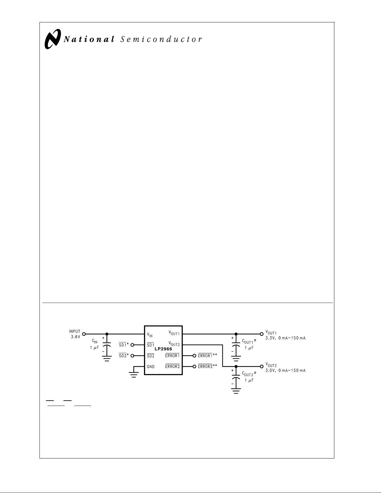
Typical Application Circuit
DS100850-30
*SD1 and SD2 must be actively terminated through a pull up resistor. Tie to VINif not used.
**ERROR1 and ERROR2 are open drain outputs. These pins must be connected to ground if not used.
# Minimum output capacitance is 1µF to insure stability over full load current range. More capacitance improves superior dynamic performance and provides
additional stability margin.
© 2000 National Semiconductor Corporation DS100850 www.national.com
Page 2
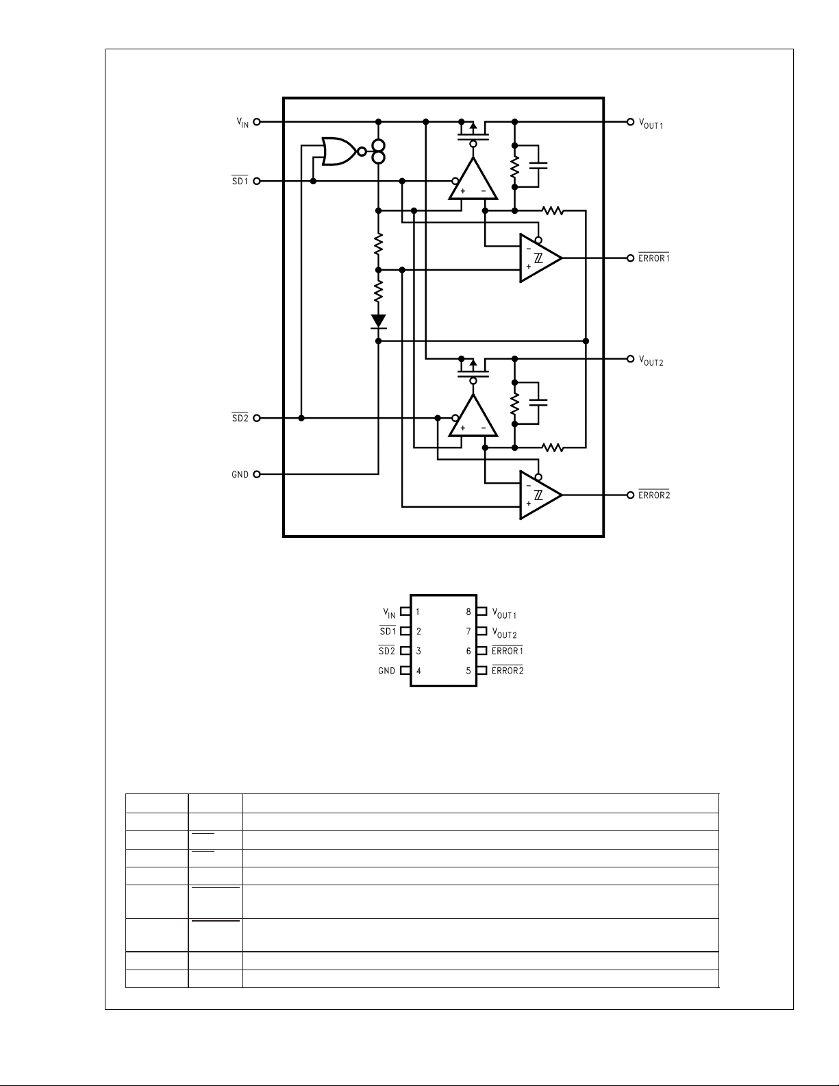
Block Diagram
LP2966 Dual 150mA Ultra Low-Dropout Regulator
Connection Diagram
Top View
Mini SO-8 Package
8-Lead Small Outline Integrated Circuit (SOIC)
Package Code: MSOP-8
Pin Description
Pin Name Function
1 VIN Input Supply pin
2 SD1
3 SD2
4 GND Ground
5 ERROR2
6 ERROR1
7 VOUT2 Output 2
8 VOUT1 Output 1
Active low shutdown pin for output 1
Active low shutdown pin for output 2
Error flag for output 2 - Normally high impedance, should be connected to ground if not
used.
Error flag for output 1 - Normally high impedance, should be connected to ground if not
used.
DS100850-31
DS100850-32
www.national.com 2
Page 3
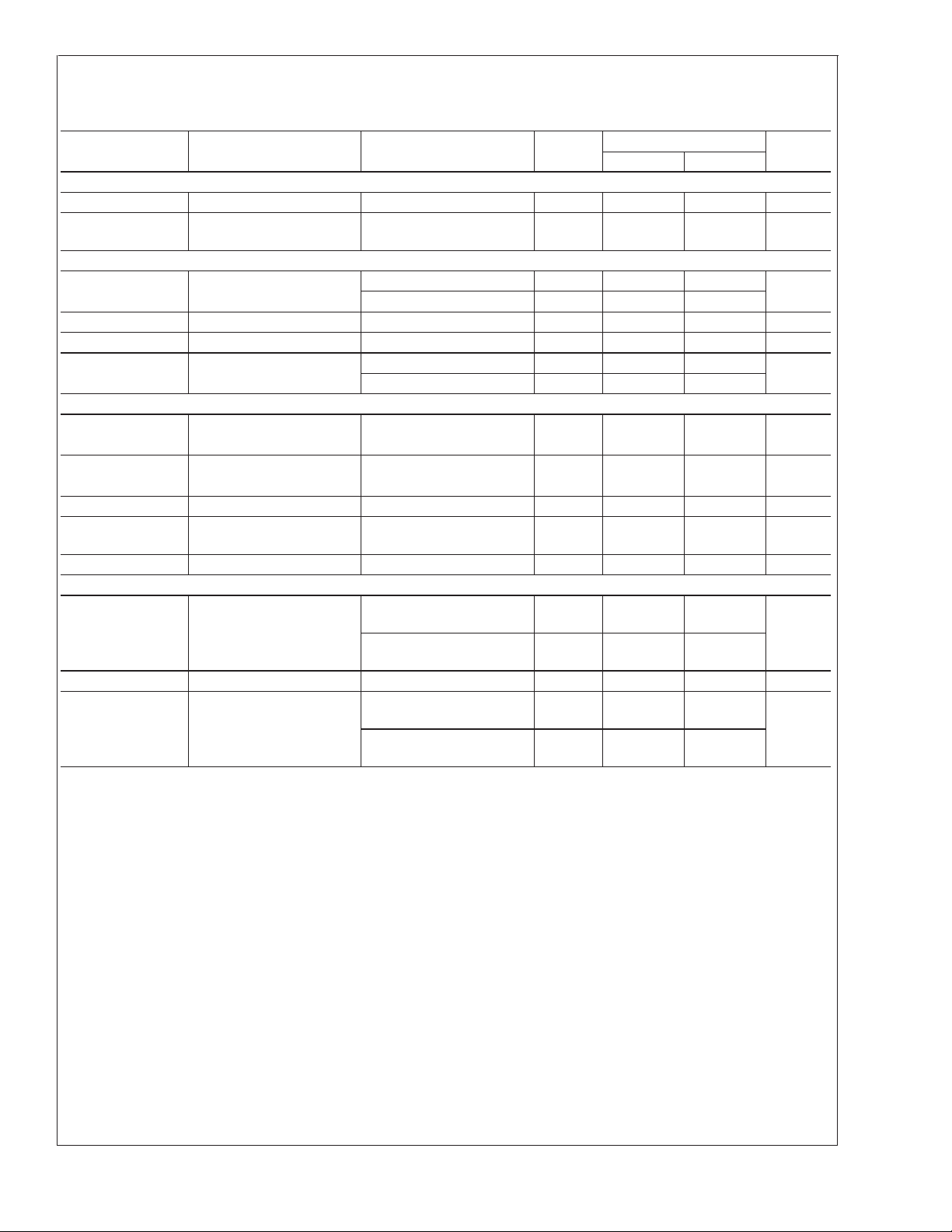
Ordering Information
The following voltage options and their combinations are possible.
5.0V, 4.0V, 3.8V, 3.6V, 3.3V, 3.2V, 3.1V, 3.0V, 2.9V, 2.8V, 2.7V, 2.6V, 2.5V, 2.4V, 2.0V and 1.8V
TABLE 1.
Output Voltage 1 Output Voltage 2 Order Number Package Marking Supplied As:
5.0 5.0 LP2966IMM-5050 LAFB 1000 units on tape and reel
5.0 5.0 LP2966IMMX-5050 LAFB 3500 units on tape and reel
3.6 3.6 LP2966IMM-3636 LAEB 1000 units on tape and reel
3.6 3.6 LP2966IMMX-3636 LAEB 3500 units on tape and reel
3.3 3.6 LP2966IMM-3336 LAHB 1000 units on tape and reel
3.3 3.6 LP2966IMMX-3336 LAHB 3500 units on tape and reel
3.3 3.3 LP2966IMM-3333 LADB 1000 units on tape and reel
3.3 3.3 LP2966IMMX-3333 LADB 3500 units on tape and reel
3.3 2.5 LP2966IMM-3325 LARB 1000 units on tape and reel
3.3 2.5 LP2966IMMX-3325 LARB 3500 units on tape and reel
3.0 3.0 LP2966IMM-3030 LACB 1000 units on tape and reel
3.0 3.0 LP2966IMMX-3030 LACB 3500 units on tape and reel
2.8 3.0 LP2966IMM-2830 LASB 1000 units on tape and reel
2.8 3.0 LP2966IMMX-2830 LASB 3500 units on tape and reel
2.8 2.8 LP2966IMM-2828 LABB 1000 units on tape and reel
2.8 2.8 LP2966IMMX-2828 LABB 3500 units on tape and reel
2.5 2.5 LP2966IMM-2525 LAAB 1000 units on tape and reel
2.5 2.5 LP2966IMMX-2525 LAAB 3500 units on tape and reel
1.8 3.3 LP2966IMM-1833 LCFB 1000 units on tape and reel
1.8 3.3 LP2966IMMX-1833 LCFB 3500 units on Tape and reel
1.8 1.8 LP2966IMM-1818 LA9B 1000 units on tape and reel
1.8 1.8 LP2966IMMX-1818 LA9B 3500 units on tape and reel
The voltage options and combinations shown in
of voltage options, please contact your nearest National Semiconductor Sales Office.
Table 1
are available. For other custom voltage options or combinations
LP2966 Dual 150mA Ultra Low-Dropout Regulator
www.national.com3
Page 4
Absolute Maximum Ratings (Note 1)
If Military/Aerospace specified devices are required,
Output Voltage (Survival)(Note 6),
(Note 7)
−0.3V to (Vin + 0.3V)
please contact the National Semiconductor Sales Office/
Distributors for availability and specifications.
Storage Temperature Range −65 to +150˚C
Lead Temp. (Soldering, 5 sec.) 260˚C
Power Dissipation (Note 2) Internally Limited
ESD Rating (Note 3) 2kV
Input Supply Voltage (Survival) −0.3V to 7.5V
Shutdown Input Voltage (Survival) −0.3V to (Vin + 0.3V)
Maximum Voltage for ERROR
10V
Operating Ratings (Note 1)
Input Supply Voltage 2.7V to 7.0V
Shutdown Input Voltage −0.3V to (Vin + 0.3V)
Operating Junction
Temperature Range
Maximum Voltage for
ERROR pins
−40˚C to +125˚C
Pins
I
(Survival) Short Circuit
OUT
Protected
Electrical Characteristics
Limits in standard typeface are for Tj= 25˚C, and limits in boldface type apply over the full operating junction temperature
range. Unless otherwise specified, V
LP2966 Dual 150mA Ultra Low-Dropout Regulator
Symbol Parameter Conditions
V
o
(Note 13)
∆V
/∆V
O
IN
(Note 8)
(Note 13)
/∆I
∆V
O
OUT
∆V
/∆I
O2
OUT1
V
IN-VOUT
I
I
I
I
(Note 18) Ground Pin Current (One
GND(1,0)
GND(1,1)
GND(0,0)
O(PK)
Short Circuit Foldback Protection
I
FB
Output Voltage Tolerance V
Output Voltage Line
Regulation
Output Voltage Load
Regulation (Note 9)
Output Voltage Cross
Regulation (Note 10)
Dropout Voltage
(Note 12)
LDO On)
Ground Pin Current (Both
LDOs On)
Ground Pin Current in
Shutdown Mode
Peak Output Current (Note 2)
Short Circuit Foldback
Knee
IN=VO(NOM)
+ 1V, (Note 16), C
+1V<V
OUT
= 1µF, I
OUT
<
7.0V 0.0 −1 1
IN
= 1mA, CIN= 1µF, V
OUT
Typ
LP2966IMM (Note 5)
(Note 4)
Min Max
SD1=VSD2=VIN
-3 3
<
1mA
<
I
100mA 0.0 −1.5 1.5
L
-3.5 3.5
0.1 mV/V
1mA<I
(Note 9)
1mA<I
<
L
L1
100mA
<
100mA
0.1 mV/mA
0.0004
(Note 10)
IL= 1mA 0.9 2.0
3.0
I
= 100mA 90 130
L
180
I
= 150mA 135 195
L
270
IL= 1mA 300
V
≤ 0.1V, V
SD2
SD1=VIN
IL= 100mA 340
V
≤ 0.1V, V
SD2
SD1=VIN
IL= 1mA 340 450
500
I
= 100mA 420 540
L
600
V
SD1=VSD2
≤ 0.1V 0.006 0.3
10
500 350
≥ V
V
OUT
OUT(NOM)
-5%
150
(Note 2), (Note 14) 600 mA
10V
.
Unit
%V
NOM
%V
NOM
mV/mA
mV
µA
µA
µA
mA
www.national.com 4
Page 5
Electrical Characteristics (Continued)
Limits in standard typeface are for Tj= 25˚C, and limits in boldface type apply over the full operating junction temperature
range. Unless otherwise specified, VIN=V
Symbol Parameter Conditions
Over Temperature Protection
Tsh(t) Shutdown Threshold 165 ˚C
Tsh(h) Thermal Shutdown
Hysteresis
Shutdown Input
V
SDT
Shutdown Threshold
(Note 15)
T
T
I
dOFF
dON
SD
Turn-off Delay (Note 17) IL= 100 mA 20 µsec
Turn-on Delay (Note 17) IL= 100 mA 25 µsec
SD Input Current VSD=V
Error Flag Comparators
V
T
Threshold (output goes
high to low)
V
TH
V
ERR(Sat)
I
EF(leak)
Threshold Hysteresis 5 28%
Error Flag Saturation I
Error Flag Pin Leakage
Current
I
(EFsink)
Error Flag Pin Sink Current 1 mA
AC Parameters
PSRR Ripple Rejection V
ρn(1/f) Output Noise Density f =120Hz 1 µV/
e
n
Note 1: Absolute maximum ratings indicate limits beyond which damage to the device may occur. Operating ratings indicate conditions for which the device is intended to be functional, but do not guarantee specific performance limits. For guaranteed specifications and test conditions, see Electrical characteristics. The guaranteed specifications apply only for the test conditions listed. Some performance characteristics may degrade when the device is not operated under the listed test
conditions.
Note 2: At elevated temperatures, devices must be derated based on package thermal resistance. The device in the surface-mount package must be derated at θ
= 235˚C/W, junction-to-ambient. Please refer to the applications section on maximum current capability for further information. The device has internal thermal protection.
Note 3: The human body model is a 100pF capacitor discharged through a 1.5kΩ resistor into each pin.
Note 4: : Typical numbers are at 25˚C and represent the most likely parametric norm.
Note 5: : Limits are 100% production tested at 25˚C. Limits over the operating temperature range are guaranteed through correlation using Statistical Quality Control
(SQC) methods. The limits are used to calculate National’s Averaging Outgoing Quality Level (AOQL).
Note 6: If used in a dual-supply system where the regulator load is returned to a negative supply, the LP2966 output must be diode-clamped to ground.
Note 7: The output PMOS structure contains a diode between the V
will turn on this diode.
Note 8: Output voltage line regulation is defined as the change in output voltage from the nominal value due to change in input line voltage.
Note 9: Output voltage load regulation is defined as the change in output voltage from the nominal value when the load current changes from 1mAto 100mA.
Note 10: Output voltage cross regulation is defined as the percentage change in the output voltage from the nominal value at one output when the load current
changes from 1mAto full load in the other output. This is an important parameter in multiple output regulators. The specification for ∆V
fication for ∆V
Note 11: Error Flag threshold and hysteresis are specified as the percentage below the regulated output voltage.
Note 12: Dropout voltage is defined as the input to output differential at which the output voltage drops 100mV below the nominal value. Drop-out voltage specifi-
cation applies only to output voltages greater than 2.7V.For output voltages below 2.7V, the drop-out voltage is nothing but the input to output differential, since the
minimum input voltage is 2.7V.
Note 13: Output voltage tolerance specification also includes the line regulation and load regulation.
O2
Output Noise Voltage (rms) BW = 10Hz − 100kHz,
/∆I
.
OUT1
+ 1V, (Note 16), C
O(NOM)
OUT
= 1µF, I
= 1mA, CIN= 1µF, V
OUT
Typ
LP2966IMM (Note 5)
(Note 4)
25
Output = Low 0 0.1
Output = High V
IN
=0V 1
V
SD
IN
1
VIN- 0.1
10 516%
(Note 11)
(Note 11)
= 100µA 0.015 0.1 V
Fsink
1nA
IN=VOUT
120Hz, V
V
IN=VOUT
120Hz, V
+ 1V, f =
= 3.3V
OUT
+ 0.3V, f =
= 3.3V
OUT
60
40
150
= 10µF
C
OUT
BW = 300Hz − 300kHz,
C
= 10µF
OUT
and V
IN
terminals that is normally reverse-biased. Reversing the polarity from VINand V
OUT
100
SD1=VSD2=VIN
Min Max
/∆I
O1
is equal to the speci-
OUT2
Unit
˚C
nA
dB
µV(rms)
.
V
√
OUT
LP2966 Dual 150mA Ultra Low-Dropout Regulator
Hz
jA
www.national.com5
Page 6

Electrical Characteristics (Continued)
Note 14: LP2966 has fold back current limited short circuit protection. The knee is the current at which the output voltage drops 10% below the nominal value.
Note 15: V
Note 16: The condition V
As an example, if Vout1 = 3.3V and Vout2 = 5V, then the condition V
Note 17: Turn-on delay is the time interval between the low to high transition on the shutdown pin to the output voltage settling to within 5% of the nominal value.
Turn-offdelay is the time interval between the high to low transition on the shutdown pin to the output voltage dropping below 50% of the nominal value. The external
load impedance influences the output voltage decay in shutdown mode.
Note 18: The limits for the ground pin current specification, I
LP2966 Dual 150mA Ultra Low-Dropout Regulator
is the shutdown pin voltage threshold below which the output is disabled.
SDT
IN=VO(NOM)
+ 1V applies when Vout1 = Vout2. If Vout1≠Vout2, then this condition would apply to the output which is greater in value.
IN=VO(NOM)
will be same as the limits for the specification, I
GND(0,1)
+ 1V would apply to Vout2 only.
GND(1,0)
.
www.national.com 6
Page 7

LP2966 Dual 150mA Ultra Low-Dropout Regulator
Typical Performance Characteristics Unless otherwise specified, V
C
=1µF, I
OUT
Ground Pin Current vs Supply Voltage (one LDO on)
Ground Pin Current vs Load Current over temperature
(one LDO on)
= 1mA, CIN=1µF, V
OUT
SD1=VSD2=VIN
DS100850-1
, and TA= 25˚C.
Ground Pin Current vs Supply Voltage (both LDOs on)
Ground Pin Current vs Load Current over temperature
(both LDOs on)
IN=VO(NOM)
+1V,V
DS100850-2
OUT
= 3.3V,
Output Voltage vs Temperature
DS100850-3
DS100850-5
DS100850-4
Drop-out Voltage vs Temperature
DS100850-6
www.national.com7
Page 8

Typical Performance Characteristics Unless otherwise specified, V
C
OUT
=1µF, I
= 1mA, CIN=1µF, V
OUT
SD1=VSD2=VIN
, and TA= 25˚C. (Continued)
IN=VO(NOM)
+ 1V, V
OUT
= 3.3V,
Input Voltage vs Output Voltage
DS100850-7
LP2966 Dual 150mA Ultra Low-Dropout Regulator
Ground Pin Current vs Input Voltage (Both LDOs off)
Ground Pin Current vs Shutdown Pin Voltage
DS100850-8
Short-Circuit Foldback Protection
Line Transient Response
(C
OUT
= 2.2µF, I
OUT
= 1mA)
DS100850-9
DS100850-18
Line Transient Response
(C
OUT
= 2.2µF, I
OUT
= 1mA)
DS100850-10
DS100850-19
www.national.com 8
Page 9

LP2966 Dual 150mA Ultra Low-Dropout Regulator
Typical Performance Characteristics Unless otherwise specified, V
C
=1µF, I
OUT
Line Transient Response
(C
= 2.2µF, I
OUT
Line Transient Response
(C
= 10µF, I
OUT
= 1mA, CIN=1µF, V
OUT
= 100mA)
OUT
= 1mA)
OUT
SD1=VSD2=VIN
DS100850-20
, and TA= 25˚C. (Continued)
Line Transient Response
(C
OUT
= 2.2µF, I
OUT
= 100mA)
Line Transient Response
(C
OUT
= 10µF, I
OUT
= 1mA)
IN=VO(NOM)
+ 1V, V
DS100850-21
OUT
= 3.3V,
Line Transient Response
(C
OUT
= 10µF, I
OUT
= 100mA)
DS100850-22
DS100850-25
Line Transient Response
(C
OUT
= 10µF, I
OUT
= 100mA)
DS100850-23
DS100850-24
www.national.com9
Page 10

Typical Performance Characteristics Unless otherwise specified, V
C
OUT
=1µF, I
= 1mA, CIN=1µF, V
OUT
SD1=VSD2=VIN
, and TA= 25˚C. (Continued)
IN=VO(NOM)
+ 1V, V
OUT
= 3.3V,
Load Transient Response (C
Load Transient Response (C
LP2966 Dual 150mA Ultra Low-Dropout Regulator
OUT
OUT
= 2.2µF)
= 10µF)
DS100850-26
Load Transient Response (C
Load Transient Response (C
OUT
OUT
= 10µF)
DS100850-27
= 2.2µF)
Cross-Channel Isolation vs Frequency
(I
OUT1
=1mA, I
OUT2
= 1mA)
DS100850-28
DS100850-15
Cross-Channel Isolation vs Frequency
(I
OUT1=IOUT2
= 100mA)
DS100850-29
DS100850-16
www.national.com 10
Page 11

LP2966 Dual 150mA Ultra Low-Dropout Regulator
Typical Performance Characteristics Unless otherwise specified, V
C
=1µF, I
OUT
Output Voltage Cross-Coupling
Power Supply Ripple Rejection
= 1mA, CIN=1µF, V
OUT
SD1=VSD2=VIN
DS100850-13
, and TA= 25˚C. (Continued)
Output Noise Density
Peak Output Current vs Temperature
IN=VO(NOM)
+ 1V, V
DS100850-14
OUT
= 3.3V,
DS100850-17
DS100850-41
www.national.com11
Page 12

Applications Information
Input Capacitor Selection
LP2966 requires a minimum input capacitance of 1µF between the input and ground pins to prevent any impedance
interactions with the supply. This capacitor should be located
very close to the input pin. This capacitor can be of any type
such as ceramic, tantalum, or aluminium. Any good quality
capacitor which has good tolerance over temperature and
frequency is recommended.
Output Capacitor Selection
The LP2966 requires a minimum of 1µF capacitance on
each output for proper operation. To insure stability, this capacitor should maintain its ESR (equivalent series resistance) in the stable region of the ESR curves (
Figure 2
plication. The output capacitor should have a good tolerance
over temperature, voltage, and frequency. The output capacitor can be increased without limit. Larger capacitance
provides better stability and noise performance. The output
capacitor should be connected very close to the Vout pin of
the IC.
LP2966 Dual 150mA Ultra Low-Dropout Regulator
FIGURE 1. ESR Curve for V
LP2966 works best with Tantalum capacitors. However, the
ESR and the capcitance value of these capacitors vary a lot
with temperature, voltage, and frequency. So while using
over the full operating temperature range of the ap-
DS100850-11
= 5V and C
OUT
DS100850-12
FIGURE 2. ESR Curve for V
= 3.3V and C
OUT
2.2µF
Figure 1
= 2.2µF
OUT
OUT
and
=
Tantalum capacitors, it should be ensured that the ESR is
within the limits for stability over the full operating temparature range.
For output voltages greater than 2.5V, good quality ceramic
capacitors (such as the X7R series from Taiyoyuden) can
also be used with LP2966 in applications not requiring light
load operation (
<
5mAfor the 5V output option). Once again,
it should be ensured that the capacitance value and the ESR
are within the limits for stability over the full operating temperature range.
The ESRD Series Polymer Aluminium Electrolytic capacitors
from Cornell Dubilier are very stable over temperature and
frequency. The excellent capacitance and ESR tolerance of
these capacitors over voltage, temperature and frequency
make these capacitors very suitable for use with LDO regulators.
Output Noise
Noise is specified in two waysSpot Noise or Output noise density is the RMS sum of all
noise sources, measured at the regulator output, at a specific frequency (measured with a 1Hz bandwidth). This type
of noise is usually plotted on a curve as a function of frequency.
Total output Noise or Broad-band noise is the RMS sum
of spot noise over a specified bandwidth, usually severaldecades of frequencies.
Attention should be paid to the units of measurement. Spot
noise is measured in units µV/
√
Hz or nV/√Hz and total output
noise is measured in µV(rms).
The primary source of noise in low-dropout regulators is the
internal reference. In CMOS regulators, noise has a low frequency component and a high frequency component, which
storngly depend on the silicon area and quiescent current.
Noise can be reduced in two ways: by increasing the transistor area or by increasing the current drawn by the internal
reference. Increasing the area will increase the die size and
decreases the chance of fitting the die into a small package.
Increasing the current drawn by the internal reference increases the total supply current (ground pin current) of the
IC. Using an optimized trade-off of ground pin current and
die size, LP2966 achieves low noise performance with low
quiescent current in an MSOP-8 package.
Short-Circuit Foldback protection
In the presence of a short or excessive load current condition, the LP2966 uses an internal short circuit foldback
mechanism that regulates the maximum deliverable output
current. A strong negative temperature coefficient is designed into the circuit to enable extremely higher peak output
current capability (in excess of 400mA per output at room
temperature, see typical curves). Thus, a system designer
using the LP2966 can achieve higher peak output current
capability in applications where the LP2966 internal junction
temperature is kept below 125˚C. Refer to the applications
section on calculating the maximum output current capability
of the LP2966 for your application.
Error Flag Operation
The LP2966 produces a logic low signal at the Error Flag pin
(ERROR) when the corresponding output drops out of regulation due to low input voltage, current limiting, or thermal
limiting. This flag has a built in Hysteresis. The timing diagram in
Figure 3
shows the relationship between the ERROR and the output voltage. In this example, the input voltage is changed to demonstrate the functionality of the Error
Flag.
www.national.com 12
Page 13

Applications Information (Continued)
FIGURE 3. Error Flag Operation
The internal error flag comparators have open drain output
stages. Hence, the ERROR pins should be pulled high
through a pull up resistor. Although the ERROR pin can sink
current of 1mA, this current adds to the battery drain. Hence,
the value of the pull up resistor should be in the range of
100kΩ to 1MΩ. The ERROR pins must be connected to
ground if this function is not used. It should also be noted
that when the shutdown pins are pulled low, the ERROR pins
are forced to be invalid for reasons of saving power in shutdown mode.
Shutdown Operation
The two LDO regulators in the LP2966 have independent
shutdown. A CMOS Logic level signal at the shutdown( SD)
pin will turn-off the corresponding regulator. Pins SD1 and
SD2 must be actively terminated through a 100kΩ pull-up resistor for a proper operation. If these pins are driven from a
source that actively pulls high and low (such as a CMOS rail
to rail comparator), the pull-up resistor is not required. These
pins must be tied to Vin if not used.
Drop-Out Voltage
The drop-out voltage of a regulator is defined as the minimum input-to-output differential required to stay within
100mV of the output voltage measured with a 1V differential.
The LP2966 uses an internal MOSFET with an Rds(on) of
1Ω. For CMOS LDOs, the drop-out voltage is the product of
the load current and the Rds(on) of the internal MOSFET.
Reverse Current Path
The internal MOSFET in the LP2966 has an inherent parasitic diode. During normal operation, the input voltage is
higher than the output voltage and the parasitic diode is reverse biased. However, if the output is pulled above the input
in an application, then current flows from the output to the input as the parasitic diode gets forward biased. The output
can be pulled above the input as long as the current in the
parasitic diode is limited to 150mA.
Maximum Output Current Capability
DS100850-35
Each output in the LP2966 can deliver a current of more than
150mA over the full operating temperature range. However,
the maximum output current capability should be derated by
the junction temperature. Under all possible conditions, the
junction temperature must be within the range specified under operating conditions. The LP2966 is available in
MSOP-8 package. This package has a junction to ambient
temperature coefficient (θ
) of 235 ˚C/W with minimum
ja
amount of copper area. The total power dissipation of the device is approximately given by:
P
=(Vin-V
D
OUT1)IOUT1
The maximum power dissipation, P
+(Vin-V
OUT2)IOUT2
, that the device can
Dmax
tolerate can be calculated by using the formula
P
=(T
Dmax
where T
jmax-TA
jmax
(125˚C), and T
)/θ
ja
is the maximum specified junction temperature
is the ambient temperature.
A
The following figures show the variation of thermal coefficient with different layout scenarios.
LP2966 Dual 150mA Ultra Low-Dropout Regulator
www.national.com13
Page 14

Applications Information (Continued)
DS100850-36
LP2966 Dual 150mA Ultra Low-Dropout Regulator
DS100850-37
DS100850-38
DS100850-39
DS100850-40
www.national.com 14
Page 15

Physical Dimensions inches (millimeters) unless otherwise noted
LP2966 Dual 150mA Ultra Low-Dropout Regulator
Mini SO-8 Package Type MM
For Ordering, Refer to Ordering Information Table
NS Package Number MUA08A
LIFE SUPPORT POLICY
NATIONAL’S PRODUCTS ARE NOT AUTHORIZED FOR USE AS CRITICAL COMPONENTS IN LIFE SUPPORT
DEVICES OR SYSTEMS WITHOUT THE EXPRESS WRITTEN APPROVAL OF THE PRESIDENT AND GENERAL
COUNSEL OF NATIONAL SEMICONDUCTOR CORPORATION. As used herein:
1. Life support devices or systems are devices or
systems which, (a) are intended for surgical implant
into the body, or (b) support or sustain life, and
whose failure to perform when properly used in
accordance with instructions for use provided in the
2. A critical component is any component of a life
support device or system whose failure to perform
can be reasonably expected to cause the failure of
the life support device or system, or to affect its
safety or effectiveness.
labeling, can be reasonably expected to result in a
significant injury to the user.
National Semiconductor
Corporation
Americas
Tel: 1-800-272-9959
Fax: 1-800-737-7018
Email: support@nsc.com
www.national.com
National Semiconductor
Europe
Fax: +49 (0) 180-530 85 86
Email: europe.support@nsc.com
Deutsch Tel: +49 (0) 69 9508 6208
English Tel: +44 (0) 870 24 0 2171
Français Tel: +33 (0) 1 41 91 8790
National Semiconductor
Asia Pacific Customer
Response Group
Tel: 65-2544466
Fax: 65-2504466
Email: ap.support@nsc.com
National Semiconductor
Japan Ltd.
Tel: 81-3-5639-7560
Fax: 81-3-5639-7507
National does not assume any responsibility for use of any circuitry described, no circuit patent licenses are implied and National reserves the right at any time without notice to change said circuitry and specifications.
 Loading...