

Datasheet LP2960IN-3.3, LP2960IMX-5.0, LP2960IMX-3.3, LP2960IM-5.0, LP2960IM-3.3 Datasheet (NSC)
...Page 1
LP2960
Adjustable Micropower 0.5A Low-Dropout Regulators
General Description
The LP2960 is a micropower voltage regulator with very low
dropout voltage (12 mV typical at 1 mA load and 470 mV
typical at 500 mA load) and very low quiescent current
(450 µA typical at 1 mA load).
The LP2960 is ideally suited for battery-powered systems:
the quiescent current increases only slightly at dropout,
which prolongs battery life.
The LP2960 retains all the desirable characteristics of the
LP2953, and offers increased output current.
The error flag goes low anytimetheoutput drops more than
5%out of regulation.
Reverse battery protection is provided.
The LP2960 requires only 10 µF of output capacitance for
stability (5V version).
The internal voltage reference is made available for external
use, providing a low-T.C. reference with very good regulation
characteristics.
The parts are available in 16-pin plastic DIP and 16-pin surface mount packages.
Features
n Output voltage adjusts from 1.23V–29V
n Guaranteed 500 mA output current
n 5V and 3.3V versions available
n 16-pin DIP and 16-pin SO packages
n Low dropout voltage
n Low quiescent current
n Tight line and load regulation
n Low temperature coefficient
n Current limiting and thermal protection
n Logic-level shutdown
n Can be wired for snap-ON and snap-OFF
n Reverse battery protection
Applications
n High-efficiency linear regulator
n Regulator with under-voltage shutdown
n Low dropout battery-powered regulator
n Cellular telephones
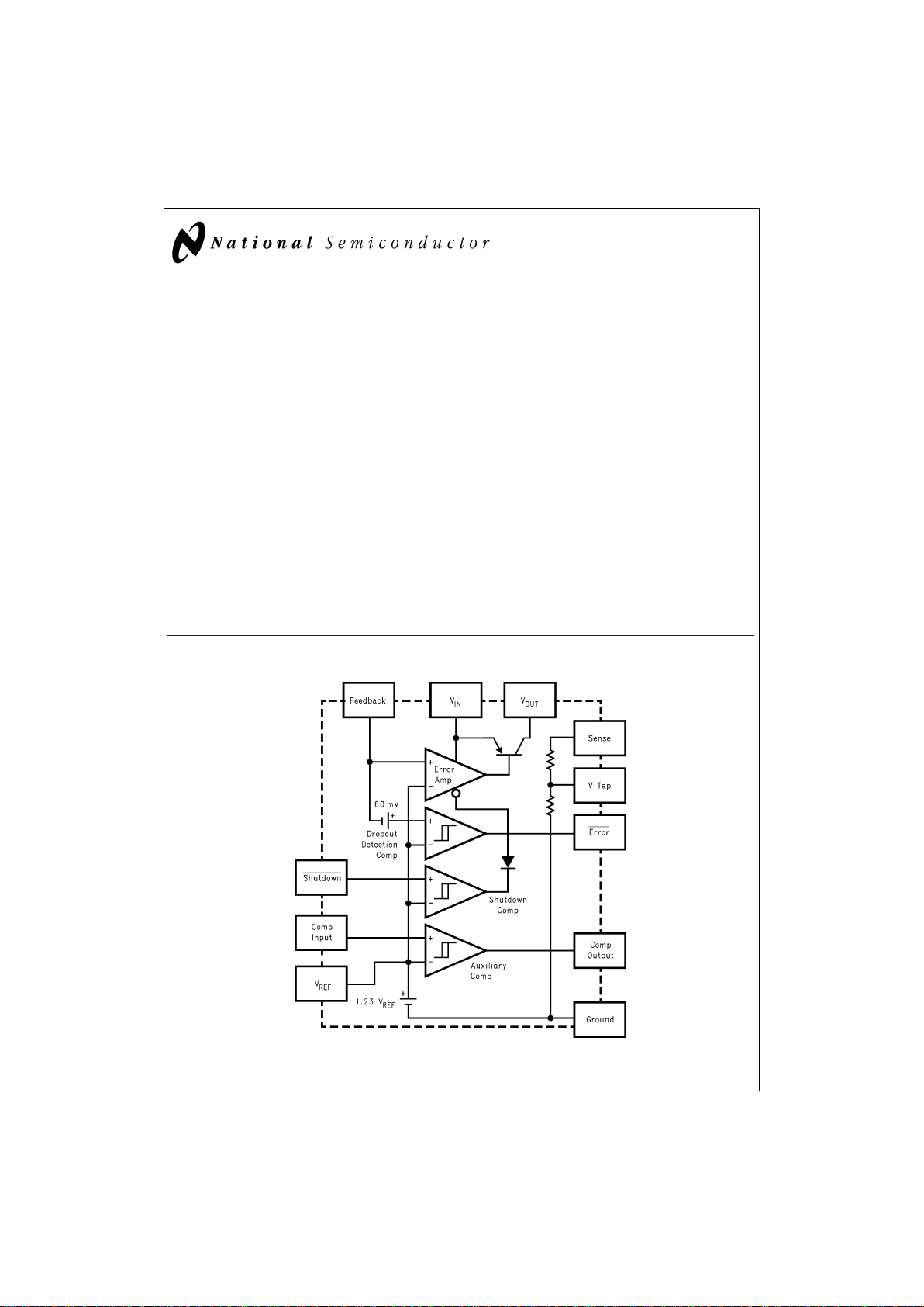
Block Diagram
DS011962-1
April 1999
LP2960 Adjustable Micropower 0.5A Low-Dropout Regulators
© 1999 National Semiconductor Corporation DS011962 www.national.com
Page 2
Absolute Maximum Ratings (Note 1)
If Military/Aerospace specified devices are required,
please contact the National Semiconductor Sales Office/
Distributors for availability and specifications.
Storage Temperature Range −65˚C to +150˚C
Operating Junction Temperature
Range
LP2960AI/LP2960I −40˚C to +125˚C
Lead Temperature (Soldering, 5 sec.) 260˚C
Power Dissipation (Note 2) Internally Limited
Input Supply Voltage −20V to +30V
Feedback Input Voltage (Note 3) −0.3V to +5V
Comparator Input Voltage (Note 4) −0.3V to +30V
Comparator Output Voltage (Note 4) −0.3V to +30V
ESD Rating (Note 15) 1.5 kV
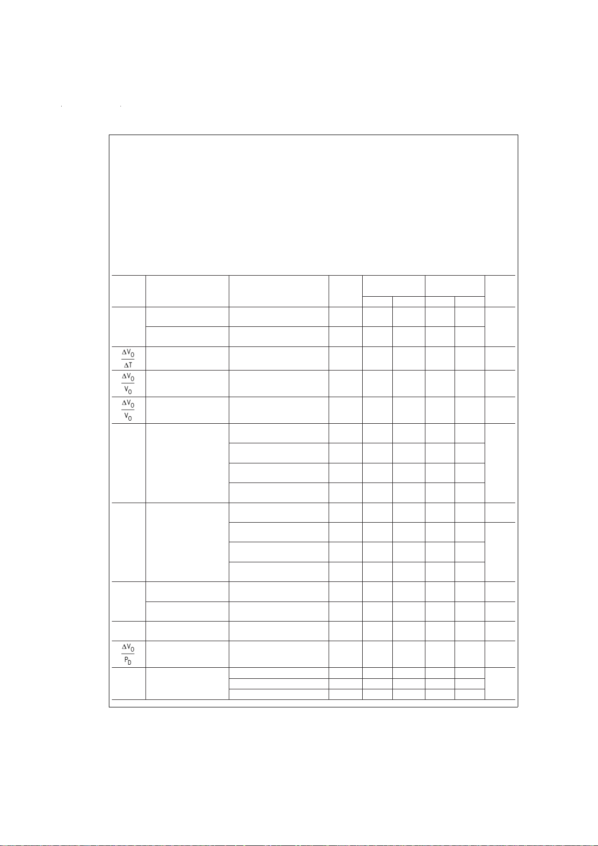
Electrical Characteristics Limits in standard typeface are for T
J
=
25˚C, and limits in boldface type apply
over the full operating temperature range. Unless otherwise specified: C
IN
=
4.7 µF, V
IN
=
V
O
(NOM) + 1V, I
L
=
1 mA,
C
OUT
=
10 µF for 5V parts or C
OUT
=
22 µF for 3.3V parts, Feedback pin is tied to V
TAP
pin, Output pin is tied to Sense pin,
V
S/D
=
2V.
Symbol Parameter Conditions Typ
LP2960AI
(Note 14)
LP2960I
(Note 14)
Units
Min Max Min Max
V
O
Output Voltage
(5V Versions)
1mA≤IL≤500 mA
5.0
4.962
4.930
5.038
5.070
4.925
4.880
5.075
5.120
V
Output Voltage
(3.3 Versions)
1mA≤I
L
≤500 mA
3.3
3.275
3.254
3.325
3.346
3.250
3.221
3.350
3.379
Output Voltage
Temperature Coefficient
(Note 5)
20 130 160 ppm/˚C
Output Voltage
Line Regulation
V
IN
=
[V
O
(NOM) + 1V] to 30V
0.06
0.2
0.5
0.4
0.8
%
Output Voltage
Load Regulation
(Note 6)
0.08
0.16
0.30
0.20
0.40
%
V
IN−VO
Dropout Voltage (Note 7) I
L
=
1mA
12
30
50
30
50
mV
I
L
=
100 mA
180
250
350
250
350
I
L
=
200 mA
260
350
450
350
450
I
L
=
500 mA
470
600
800
600
800
I
GND
Ground Pin Current
(Note 8)
I
L
=
1mA
450
600
750
600
750
µA
I
L
=
100 mA
2.6
4.0
5.0
4.0
5.0
mA
I
L
=
200 mA
2.5
8
10
8
10
I
L
=
500 mA
21
35
40
35
40
I
GND
Ground Pin Current
at Dropout (Note 8)
V
IN
=
V
O
(NOM) − 0.5V
I
L
=
100 µA
1.8
3
5
3
5
mA
Ground Pin Current
at Shutdown (Note 8)
V
SD
≤ 1.1V
300 400 400 µA
I
LIMIT
Current Limit R
L
=
0.5Ω
1000
1500
1600
1500
1600
mA
Thermal Regulation (Note 10)
0.05 0.2 0.2
%
/W
e
n
Output Noise Voltage
@
I
L
=
100 mA
(10 Hz–100kHz)
C
OUT
=
10 µF 300
µV RMSC
OUT
=
47 µF 210
C
OUT
=
47 µF (Note 11) 130
www.national.com 2
Page 3
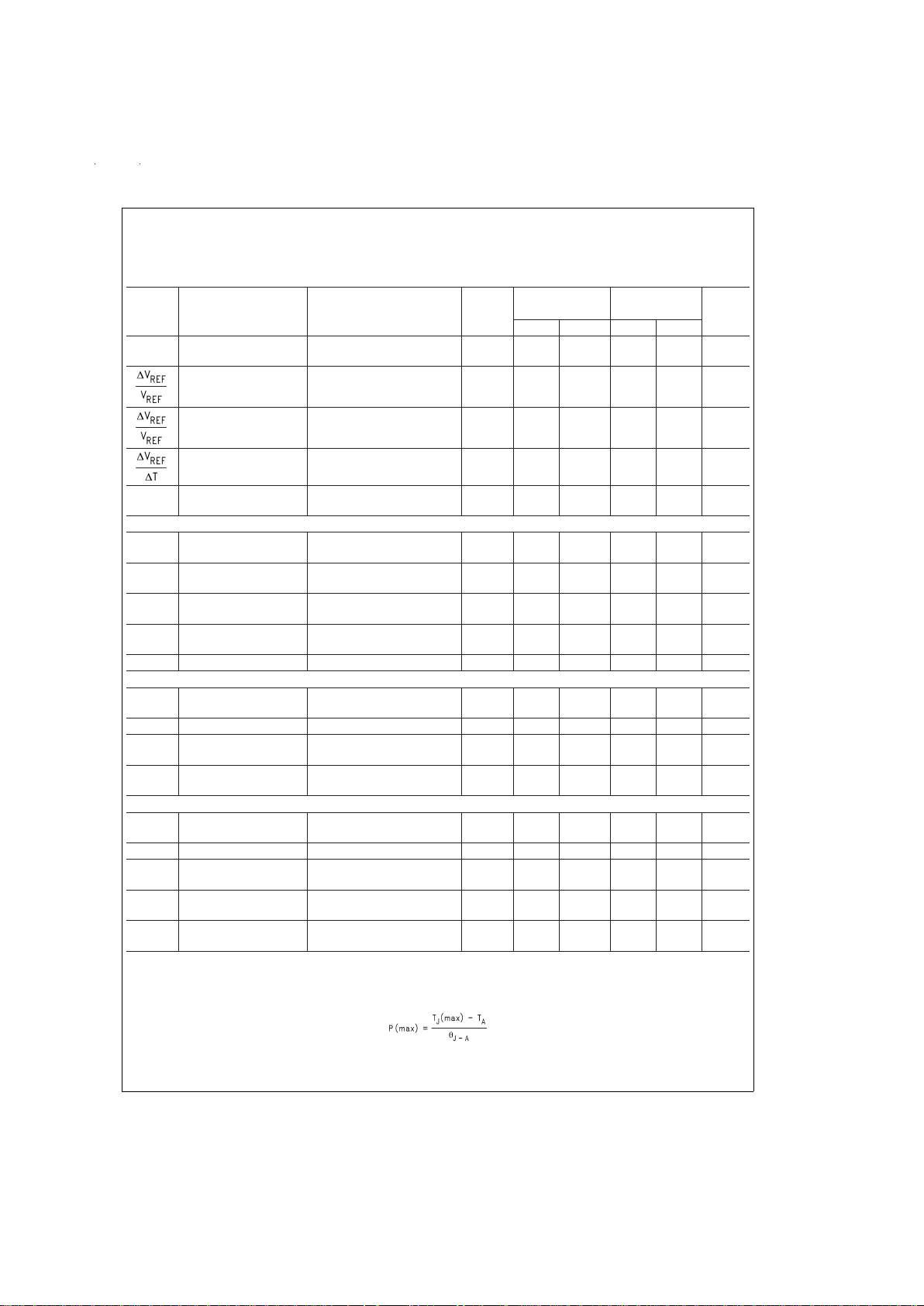
Electrical Characteristics Limits in standard typeface are for T
J
=
25˚C, and limits in boldface type apply
over the full operating temperature range. Unless otherwise specified: C
IN
=
4.7 µF, V
IN
=
V
O
(NOM) + 1V, I
L
=
1 mA,
C
OUT
=
10 µF for 5V parts or C
OUT
=
22 µF for 3.3V parts, Feedback pin is tied to V
TAP
pin, Output pin is tied to Sense pin,
V
S/D
=
2V. (Continued)
Symbol Parameter Conditions Typ
LP2960AI
(Note 14)
LP2960I
(Note 14)
Units
Min Max Min Max
V
REF
Reference Voltage
1.235
1.220
1.210
1.250
1.265
1.210
1.195
1.260
1.275
V
Reference Voltage
Line Regulation
(Note 13)
0.05
0.1
0.30
0.2
0.4
%
Reference Voltage
Load Regulation
I
REF
=
0–200 µA
0.45
0.6
0.9
1.2
1.5
%
Reference Voltage
Temperature Coefficient
(Note 5)
20 ppm/˚C
I
B
(FB) Feedback Pin Bias
Current
−20
−50
−70
−50
−70
nA
DROPOUT DETECTION COMPARATOR
I
OH
Output HIGH Leakage V
OH
=
30V
0.01
1
2
1
2
µA
V
OL
Output LOW Voltage V
IN
=
V
O
(NOM) − 1V
I
O
(COMP)=400 µA
125
250
400
250
400
mV
V
THR
(max) Upper Threshold Voltage (Note 9)
−60
−80
−100
−35
−25
−80
−100
−35
−25
mV
V
THR
(min) Lower Threshold Voltage (Note 9)
−85
−130
−200
−70
−35
−130
−200
−70
−35
mV
HYST Hysteresis (Note 9) 25 mV
SHUTDOWN INPUT
V
OS
Input Offset Voltage (Referred to V
REF
)
±
5
−18
−24
18
24
−18
−24
18
24
mV
HYST Hysteresis (Referred to V
REF
)10 mV
I
B
Input Bias Current V
S/D
=
0–5V
−20
−60
−10060100
−60
−10060100
nA
I
OUT
(S/D) Regulator Output Current
in Shutdown
(Note 12)
3
12
20
12
20
µA
AUXILIARY COMPARATOR
V
OS
Input Offset Voltage (Referred to V
REF
)
±
5
−15
−20
15
20
−15
−20
15
20
mV
HYST Hysteresis (Referred to V
REF
)10 mV
I
B
Input Bias Current V
COMP
=
0–5V
−20
−60
−10060100
−60
−10060100
nA
I
OH
Output HIGH Leakage V
OH
=
30V
V
COMP
=
1.3V
0.01
1
2
1
2
µA
V
OL
Output LOW Voltage V
COMP
=
1.1V
I
O
=
400 µA
125
250
400
250
400
mV
Note 1: Absolute maximum ratings indicate limits beyond which damage to the component may occur. Electrical specifications do not apply when operating the device outside of its rated operating conditions.
Note 2: The maximum allowable power dissipation is a function of the maximum junction temperature, T
J
(max), the junction-to-ambient thermal resistance, θ
J−A
,
and the ambient temperature, T
A
. The maximum allowable power dissipation at any ambient temperature is calculated using:
Exceeding the maximum allowable power dissipation will cause excessive die temperature, and the regulator will go into thermal shutdown. See APPLICATION
HINTS for additional information on heatsinking and thermal resistance.
Note 3: When used in dual-supply systems where the regulator load is returned to a negative supply, the output voltage must be diode-clamped to ground.
www.national.com3
Page 4

Electrical Characteristics Limits in standard typeface are for T
J
=
25˚C, and limits in boldface type apply
over the full operating temperature range. Unless otherwise specified: C
IN
=
4.7 µF, V
IN
=
V
O
(NOM) + 1V, I
L
=
1 mA,
C
OUT
=
10 µF for 5V parts or C
OUT
=
22 µF for 3.3V parts, Feedback pin is tied to V
TAP
pin, Output pin is tied to Sense pin,
V
S/D
=
2V. (Continued)
Note 4: May exceed the input supply voltage.
Note 5: Output or reference voltage temperature coefficient is defined as the worst case voltage change divided by the total temperature range.
Note 6: Output voltage load regulation is measured at constant junction temperature using low duty cycle pulse testing. Two separate tests are performed, one for
the load current range of 100 µA to 1 mA and one for the 1 mA to 500 mA range. Changes in output voltage due to heating effects are covered by the thermal regulation specification.
Note 7: Dropout voltage is defined as the input to output differential at which the output voltage drops 100 mV below the value measured with a 1V differential. At
very low values of programmed output voltage, the input voltage minimum of 2V (2.3V over temperature) must be observed.
Note 8: Ground pin current is the regulator quiescent current. The total current drawn from the source is the sum of the ground pin current, output load current, and
current through the external resistive divider (if used).
Note 9: Dropout detection comparator threshold voltages are expressed in terms of a voltage differential measured at the Feedback terminal below the
nominal
ref-
erence voltage, which is the reference voltage measured with V
IN
=
V
O
(NOM) + 1V.To express these thresholds in terms of output voltage change, multiply by the
error amplifier gain which is V
O/VREF
=
(R1 + R2)/R2 (see
Basic Application Circuit
).
Note 10: Thermal regulation is the change in output voltage at a time T after a change in power dissipation, excluding load or line regulation effects. Specifications
are for a 400 mA load pulse at V
IN
=
V
O
(NOM) + 15V (6W pulse) for T=10 ms.
Note 11: Connect a 0.1 µF capacitor from the output to the feedback pin.
Note 12: Vshutdown ≤ 1.1V, V
IN
<
30V, V
OUT
=
0V.
Note 13: Two separate tests are performed for referenc e voltage line regulation, one covering 2.5V ≤ V
IN
≤ VO(NOM) + 1V and the other test for VO(NOM) + 1V
≤ V
IN
≤ 30V.
Note 14: All room temperature limits are 100%production tested.Alllimitsattemperature extremes are guaranteed via correlation using standard Statistical Quality
Control (SQC) methods. All limits are used to calculate Average Outgoing Quality Level.
Note 15: Human Body Model, 200 pF discharged through 1.5 kΩ.
www.national.com 4
Page 5
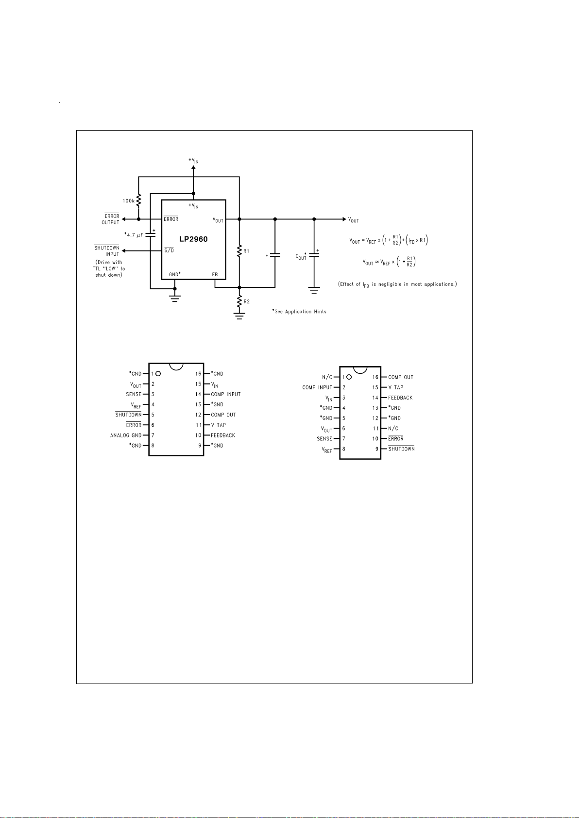
Basic Application Circuit
Connection Diagrams and Ordering Information
DS011962-2
16-Pin Surface Mount Package
DS011962-3
Top View
Order Number LP2960IM-5.0, LP2960AIM-5.0,
LP2960IM-3.3 or LP2960AIM-3.3
See NS Package Number M16A
16-Pin DIP Package
DS011962-4
Top View
Order Number LP2960IN-5.0, LP2960AIN-5.0,
LP2960IN-3.3 or LP2960AIN-3.3
See NS Package Number N16G
*
Internally Connected to Power Ground
www.national.com5
Page 6
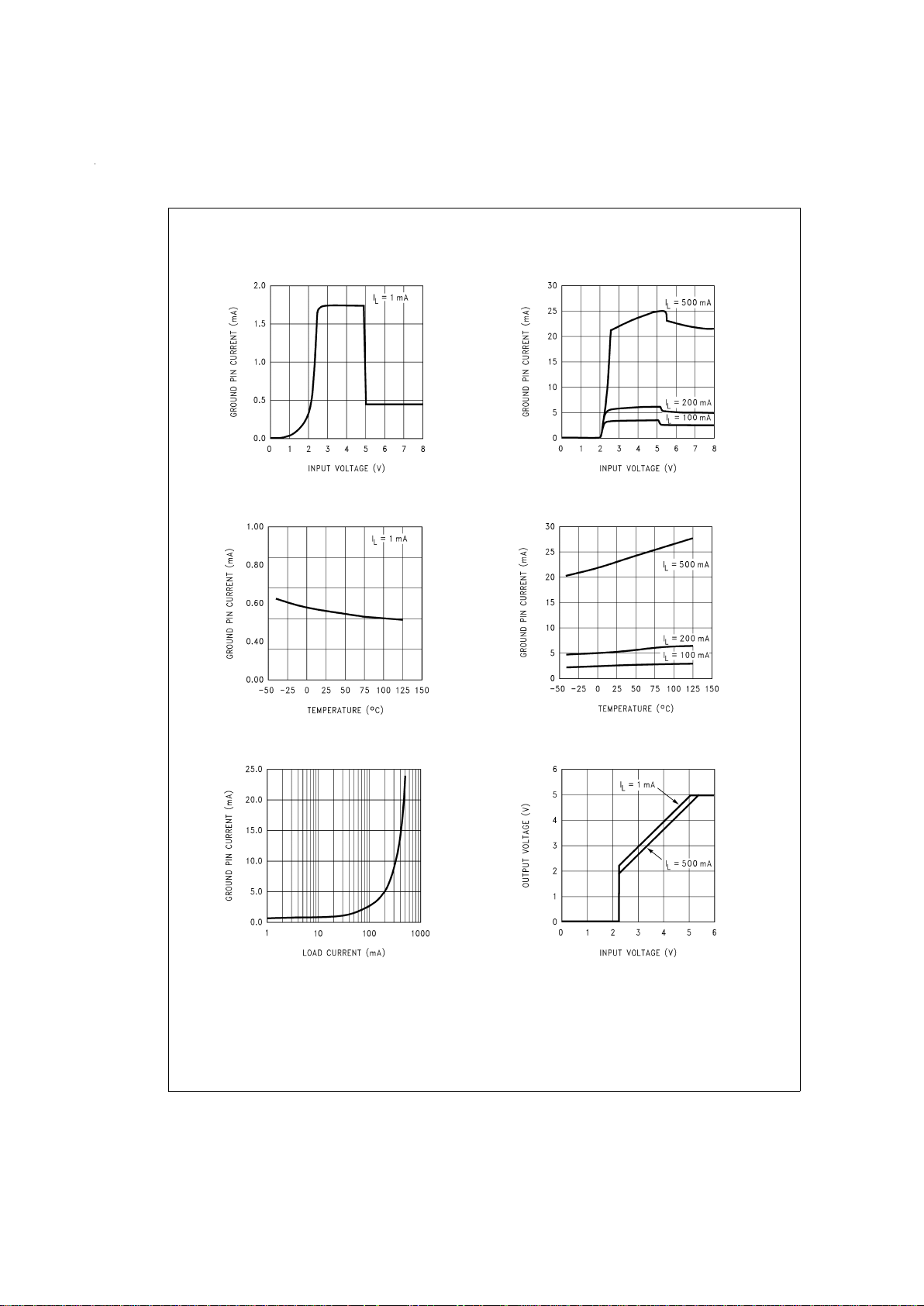
Typical Performance Characteristics Unless otherwise specified: C
IN
=
4.7 µF, V
IN
=
6V, I
L
=
1 mA,
C
OUT
=
10 µF, Feedback pin is tied to V
TAP
pin, Output pin is tied to Sense pin, V
S/D
=
2V, V
OUT
=
5V.
Ground Pin Current
DS011962-5
Ground Pin Current
DS011962-6
Ground Pin Current
DS011962-7
Ground Pin Current
DS011962-8
Ground Pin Current
DS011962-9
Dropout Characteristics
DS011962-10
www.national.com 6
Page 7

Typical Performance Characteristics Unless otherwise specified: C
IN
=
4.7 µF, V
IN
=
6V, I
L
=
1 mA,
C
OUT
=
10 µF, Feedback pin is tied to V
TAP
pin, Output pin is tied to Sense pin, V
S/D
=
2V, V
OUT
=
5V. (Continued)
Dropout Voltage vs Temperature
DS011962-11
Dropout Voltage vs Load Current
DS011962-12
Enable Transient
DS011962-13
Enable Transient
DS011962-14
Load Transient
DS011962-15
Load Transient
DS011962-16
www.national.com7
Page 8

Typical Performance Characteristics Unless otherwise specified: C
IN
=
4.7 µF, V
IN
=
6V, I
L
=
1 mA,
C
OUT
=
10 µF, Feedback pin is tied to V
TAP
pin, Output pin is tied to Sense pin, V
S/D
=
2V, V
OUT
=
5V. (Continued)
Current Limit vs Temperature
DS011962-17
Line Transient Response
DS011962-18
Line Transient Response
DS011962-19
Ripple Rejection
DS011962-20
Ripple Rejection
DS011962-21
Thermal Regulation
DS011962-22
www.national.com 8
Page 9

Typical Performance Characteristics Unless otherwise specified: C
IN
=
4.7 µF, V
IN
=
6V, I
L
=
1 mA,
C
OUT
=
10 µF, Feedback pin is tied to V
TAP
pin, Output pin is tied to Sense pin, V
S/D
=
2V, V
OUT
=
5V. (Continued)
Output Impedance
DS011962-23
Output Noise Voltage
DS011962-24
Feedback Bias Current
DS011962-25
Divider Resistance
DS011962-26
Error Output Voltage vs Input Voltage
DS011962-27
Dropout Detection Comparator
Threshold Voltage
DS011962-28
www.national.com9
Page 10

Schematic Diagram
DS011962-38
www.national.com 10
Page 11

Application Hints
EXTERNAL CAPACITORS
Bypass capacitors on the input and output of the LP2960 are
required: without these capacitors,
the part will oscillate
.
A capacitor (whose value is
at least
4.7 µF) must be con-
nected from the V
IN
pin to ground. If the input capacitor is located more than one inch away from the LP2960, the capacitor may have to be increased to 22 µF to assure stability. A
capacitor is also required between V
OUT
and Ground, and
the minimum amount of capacitance required here depends
on output voltage.
If the output voltage of the LP2960 is set to 5V,a minimum of
10 µF is needed in output capacitance. At 3.3V output, at
least 22 µF is required to assure stability.
ESR LIMIT: The ESR of the capacitor used on the LP2960
must be less than 0.7Ω
throughout the entire operating tem-
perature range
to assure stability.
The ESR of an aluminum eIectroIytic capacitor is typically
only specified at 25˚C, and does not reflect the maximum
ESR that can be expected to occur over the entire temperature range of the capacitor.
Aluminum electrolytics show a marked increase in ESR at
low temperatures (ESR can increase by a factor of 30 or
more when going from 25˚C to −30˚C) which could lead to
oscillation probIems in applications with very low ambient
temperatures. Solid tantalum capacitors are recommended
for use in such cases.
Regulator instability can be caused by stray (board layout)
capacitance appearing at the Feedback terminal. Oscillations from this effect are most Iikely to occur when very high
value resistors are used to set the output voltage.
Adding a 100 pF capacitor between the Output and Feedback pins and increasing the output capacitor to at least
22 µF will stop the osciIIations.
MINIMUM LOAD
The internal resistive divider in the LP2960 provides sufficient output loading for proper regulation. If externaI resistors are used to set the LP2960 output voltage, a minimum
current of 5 µA through the externaI resistive divider is recommended.
It should be noted that a minimum load current is specified in
several of the test conditions listed under
Electrical Charac-
teristics,
and this value of load current must be used to get
correlation on these test limits.
PROGRAMMING THE OUTPUT VOLTAGE
The LP2960 regulator may be pin-strapped for operation at
the nominal output voltage using its internal resistive divider
by tying the Output and Sense pins together and also tying
the Feedback and V
TAP
pins together.
Alternatively,it may be programmed for any voltage between
the 1.23V reference and the 30V maximum rating using an
external pair of resistors (see Basic Application Circuit).
The complete equation for the output voltage is:
V
OUT
=
V
REF
x (1 + R1/R2) + (IFBx R1)
The term V
REF
is the 1 .23V reference and IFBis the Feedback pin bias current (−20 nA typical). The minimum recommended load current of 5 µAsets an upper limit of 240 kΩ on
the value of R2 in cases where the regulator must work with
no load (see
Minimum Load
).
For best output accuracy, choosing R2=100 kΩ will reduce
the error resulting from I
FB
to 0.17%while increasing the re-
sistive divider current to 12 µA. Since the typicaI quiescent
current of the LP2960 is 450 µA, this added current through
R2 is negligible.
DROPOUT VOLTAGE
The dropout voltage of the regulator is defined as the minimum input-to-output voltage differential required for the output voltage to stay within 100 mV of the output voltage measured with a 1V differential. The dropout voltage is
independent of the programmed output voltage.
OUTPUT ISOLATION
If the LP2960 output is connected to an active voltage
source (such as a battery) the regulator input should not be
shorted to ground, as this will cause a large current to flow
from the battery into the LP2960 output lead.
If the LP2960 input is
left floating
with the output connected
to a battery,a small current (a few mA) will flow into the output lead.
The “reverse” current flowing from the battery into the
LP2960 output can be prevented by using a blocking diode
between the output and the battery.
REDUCING OUTPUT NOISE
In reference applications it may be desirabIe to reduce the
AC noise present on the output. One method is to reduce
regulator bandwidth by increasing output capacitance. This
is relatively inefficient, since large increases in capacitance
are required to get significant improvement.
Noise can be reduced more effectively by a bypass capacitor
placed across R1 (refer to
Basic Application Circuit
).
A 0.1 µF capacitor connected across R1 will reduce the high
frequency gain of the circuit to unity, lowering the RMS output noise voltage from 210 µV to 130 µV (typical) using a 10
Hz–100 kHz bandwidth test measurement.
Also, output noise is no longer proportional to the output voltage, so improvements are more pronounced at higher output
voltages.
IMPORTANT: Since the 0.1 µF capacitor reduces the AC
gain of the LP2960 to unity, the output capacitance must be
increased to at least 33 µF to assure regulator stability.
DROPOUT DETECTION COMPARATOR
The dropout detection comparator produces a logic “LOW”
on the Error output whenever the LP2960 output drops out of
regulation by more than about 5%. This figure results from
the comparator’s built-in offset of 60 mV divided by the 1.23V
reference (refer to block diagram).
The “5%below nominal” trip level remains constant regardless of the programmed output voltage. An out-of-regulation
condition can result from low input voltage, current limiting,
or thermal limiting.
The figure below gives a timing diagram showing the relationship between the output voltage, the Error output, and input voltage as the input voltage is ramped up and down to a
regulator programmed for 5V output.
www.national.com11
Page 12

Application Hints (Continued)
The Error signal becomes low as V
IN
exceeds about 1.3V.It
goes high at about 5V input, where the output equals 4.75V.
Since the dropout voltage is load dependent, the
input volt-
age
trip points will vary with load current, but the
output volt-
age
trip point does not.
The comparator has an open-collector output which requires
an external pull-up resistor. This resistor may be connected
to the LP2960 output or another supply voltage.
Best operation is obtained by connecting the pull-up to the
LP2960 output. If the pull-up resistor is connected to an external 5V supply, the error flag will incorrectly signal “HIGH”
whenever V
IN
<
1.3V (see
Error Output Timing Diagram
).
In selecting a value for the pull-up resistor, note that while
the output can sink 400 µA, this current adds to battery drain.
Suggested values range from 100 kΩ–1 MΩ. The resistor is
not required if the output is unused.
If a large output capacitance is used, a false logic “HIGH”
can be generated when V
IN
≈1.3V.In this case, the error output becomes a high impedance, causing the voltage at the
error output to rise to its pull-up value. If the pull-up resistor
is connected to V
OUT
, the error output can rise to 1.2V
(which is a logic “HIGH” signal
incorrectly
signifying the out-
put is in regulation).
The user may wish to divide down the error flag voltage us-
ing equal-value resistors (10 kΩ suggested) to ensure a
low-level logic signal during any fault condition, while still allowing a valid high logic level during normal operation.
AUXILIARY COMPARATOR
The LP2960 contains an auxiliary comparator whose inverting input is connected to the 1.23V reference. The auxiIiary
comparator has an open-collector output whose electrical
characteristics are similar to the dropout detection comparator. The non-inverting input and output are brought out for
external connections.
SHUTDOWN INPUT
A logic-level signal will shut off the regulator output when a
“LOW” (
<
1.2V) is applied to the Shutdown input.
To prevent possible mis-operation, the Shutdown input must
be actively terminated. If the input is driven from
open-collector logic, a pull-up resistor (20 kΩ–100 kΩ recommended) should be connected from the Shutdown input
to the regulator input.
If the Shutdown input is driven from a source which actively
pulls low and high (like an op-amp), the puIl-up resistor is not
required, but may be used.
If the Shutdown input is to be unused, the cost of the pull-up
resistor can be saved by tying the Shutdown input directly to
the regulator input.
IMPORTANT: Since the Absolute Maximum Ratings state
that the Shutdown input can not go more than 0.3V below
ground, the reverse-battery protection feature which protects
the regulator input is sacrificed if the Shutdown input is tied
directly to the regulator input.
If reverse-battery protection is required in an application,
the
pull-up resistor between the Shutdown input and the regulator input must be used
.
GROUND CONNECTIONS
The pins designated GND (see
Connection Diagrams
) must
be connected to the high-current ground point in the circuit.
The GND pins are electrically connected (through the lead
frame) to the die substrate, making them ideal for conducting
ground current or heat (see
Heatsinking
).
The parts in the surface-mount (M) package also have an
Analog Ground pin, which is the ground point on the die for
the regulator reference circuitry.
Along with the Sense pin, the availability of the Analog
Ground pin allows the designer the ability to use “remote”
sensing and eliminate output voltage errors due to IR drops
occurring along PC board traces.
IMPORTANT: The Analog Ground pin must be connected to
circuit ground at some point for the regulator to operate.
If remote sensing is not needed, the Analog Ground pin can
simply be pin-strapped to the adjacent GND pin.
HEATSINKING
A heatsink may be required with the LP2960 depending on
the maximum power dissipation and maximum ambient temperature of the application. Under alI possible operating conditions, the junction temperature must be within the range
specified under Absolute Maximum Ratings.
To determine if a heatsink is required, the power dissipated
by the regulator, P
D
, must be calculated.
The figure below shows the voltages and currents which are
present in the circuit, as welI as the formula for calcuIating
the power dissipated in the regulator:
Error Output Timing Diagram
DS011962-29
*
In shutdown mode, ERROR will go high if it has been pulled up to an
external supply. To avoid this invalid response, pull-up to regulator output.
**
Exact value depends on dropout voltage. (See Application Hints)
Power Dissipation Diagram
DS011962-30
www.national.com 12
Page 13

Application Hints (Continued)
The next parameter which must be calculated is the maximum allowable temperature rise, T
R
(max). This is calcu-
lated by using the formula:
T
R
(max)=TJ(max) − TA(max)
where:
T
J
(max) is the maximum allowable junction temperature,
which is 125˚C for commercial grade parts.
T
A
(max) is the maximum ambient temperature which will be
encountered in the application.
Using the calculated values for T
R
(max) and PD, the maximum allowable value for the junction-to-ambient thermal resistance, θ
(J−A)
, can now be found:
θ
(J−A)
=
T
R
(max)/P
D
The heatsink for the LP2960 is made using the PC board
copper, with the heat generated on the die being conducted
through the lead frame and out to the pins which are soldered to the PC board.
The GND pins are the only ones capable of conducting any
significant amount of heat, as they are internally attached to
the lead frame on which the die is mounted.
The figure below shows recommended copper foil patterns
to be used for heatsinking the DIP and Surface Mount packages:
The table below shows measured values of θ
(J−A)
foraPC
board with 1 ounce copper weight:
Package L (in.) H (in.) θ
J−A
(˚C/W)
DIP
1 0.5 50
2 0.2 52
Surface
Mount
1 0.5 72
2 0.2 74
As the heat must transfer from the copper to the surrounding
air, best results (lowest θ
J−A
) will be obtained by using a
sur-
face
copper layer with the solder resist opened up over the
heatsink area.
If an
internal
copper layer of a multi-layer board is used for
heatsinking, the board material acts as an insulator, inhibiting heat transfer and increasing θ
J−A
.
As with any heatsink, increasing the airflow across the board
will significantly improve the heat transfer.
Heat Sink Foil Patterns
DS011962-31
www.national.com13
Page 14

Typical Applications
Low T.C. Current Sink
DS011962-32
5V Bus Current Limiter with Load Fault Indicator
DS011962-33
*
Output voltage equals +VINminus dropout voltage, which varies with
output current. Current limits at a maximum of 1000 mA (typical).
**
Select R1 so that the comparator input voltage is 1.23V at the output
voltage which corresponds to the desired fault current value.
5V Regulator with Error Flags for Low
BATTERY and OUT OF REGULATION
DS011962-34
*
Connect to Logic or µP control inputs.
LOW BATT flag warns the user that the battery has discharged down to
about 5.8V, giving the user time to recharge the battery or power-down
some hardware with high power requirements. The output is still in
regulation at this time.
OUT OF REGULATION flag indicates when the battery is almost
completely discharged, and can be used to initiate a power-down
sequence.
5V Regulator with Snap-ON/Snap-OFF
Feature and Hysteresis
DS011962-35
*
Turns ON at V
IN
=
5.87V
Turns OFF at V
IN
=
5.64V
(for component values shown)
www.national.com 14
Page 15

Typical Applications (Continued)
5V Regulator with Timed Power-On Reset
DS011962-36
Timing Diagram for Timed Power-On Reset
DS011962-37
*
R
T
=
1 Meg, C
T
=
0.1 µF
www.national.com15
Page 16

Physical Dimensions inches (millimeters) unless otherwise noted
Order Number LP2960IM-5.0, LP2960AIM-5.0,
LP2960IM-3.3 or LP2960AIM-3.3
NS Package Number M16A
Order Number LP2960IN-5.0, LP2960AIN-5.0,
LP2960IN-3.3 or LP2960AIN-3.3
NS Package Number N16G
www.national.com 16
Page 17

Notes
LIFE SUPPORT POLICY
NATIONAL’S PRODUCTS ARE NOT AUTHORIZED FOR USE AS CRITICAL COMPONENTS IN LIFE SUPPORT
DEVICES OR SYSTEMS WITHOUT THE EXPRESS WRITTEN APPROVAL OF THE PRESIDENT AND GENERAL
COUNSEL OF NATIONAL SEMICONDUCTOR CORPORATION. As used herein:
1. Life support devices or systems are devices or
systems which, (a) are intended for surgical implant
into the body, or (b) support or sustain life, and
whose failure to perform when properly used in
accordance with instructions for use provided in the
labeling, can be reasonably expected to result in a
significant injury to the user.
2. A critical component is any component of a life
support device or system whose failure to perform
can be reasonably expected to cause the failure of
the life support device or system, or to affect its
safety or effectiveness.
National Semiconductor
Corporation
Americas
Tel: 1-800-272-9959
Fax: 1-800-737-7018
Email: support@nsc.com
National Semiconductor
Europe
Fax: +49 (0) 1 80-530 85 86
Email: europe.support@nsc.com
Deutsch Tel: +49 (0) 1 80-530 85 85
English Tel: +49 (0) 1 80-532 78 32
Français Tel: +49 (0) 1 80-532 93 58
Italiano Tel: +49 (0) 1 80-534 16 80
National Semiconductor
Asia Pacific Customer
Response Group
Tel: 65-2544466
Fax: 65-2504466
Email: sea.support@nsc.com
National Semiconductor
Japan Ltd.
Tel: 81-3-5639-7560
Fax: 81-3-5639-7507
www.national.com
LP2960 Adjustable Micropower 0.5A Low-Dropout Regulators
National does not assume any responsibility for use of any circuitry described, no circuit patent licenses are implied and National reserves the right at any time without notice to change said circuitry and specifications.
 Loading...