

Page 1

LP2957/LP2957A
5V Low-Dropout Regulator for µP Applications
LP2957/LP2957A 5V Low-Dropout Regulator for µP Applications
June 1998
General Description
The LP2957 is a 5V micropower voltage regulator with electronic shutdown, error flag, very low quiescent current
(150 µA typical at 1 mA load), and very low dropout voltage
(470 mV typical at 250 mA load current).
Output can be wired for snap-on/snap-off operation to eliminate transitionvoltage states where µP operation may be unpredictable.
Output crowbar (50 mA typical pull-down current) will bring
down the output quickly when the regulator snaps off or
when the shutdown function is activated.
The part has tight line and load regulation (0.04%typical)
and low output temperature coefficient (20 ppm/˚C typical).
The accuracy of the 5V output is guaranteed at room temperature and over the full operating temperature range.
The LP2957 is available in the five-lead TO-220 and TO-263
packages.
Package Outline
Bent, Staggered Leads
5-Lead TO-220 (T)
Order Number LP2957AIT or LP2957IT
See NS Package Number T05D
Features
n 5V output within 1.4%over temperature (A grade)
n Easily programmed for snap-on/snap-off output
n Guaranteed 250 mA output current
n Extremely low quiescent current
n Low Input-Output voltage required for regulation
n Reverse battery protection
n Extremely tight line and load regulation
n Very low temperature coefficient
n Current and thermal limiting
n Error flag signals when output is out of regulation
Applications
n High-efficiency linear regulator
n Battery-powered regulator
DS011340-16
Top View
Plastic Surface Mount Package
5-Lead TO-263 (S)
DS011340-17
Top View
DS011340-18
Order Number LP2957AIS or LP2957IS
See NS Package Number TS5B
© 1999 National Semiconductor Corporation DS011340 www.national.com
Side View
Page 2

Absolute Maximum Ratings (Note 1)
If Military/Aerospace specified devices are required,
please contact the National Semiconductor Sales Office/
Distributors for availability and specifications.
Operating Junction
Temperature Range −40˚C to +125˚C
Storage Temperature Range −65˚C to +150˚C
Lead Temperature
(Soldering, 5 Seconds) 260˚C
Power Dissipation (Note 2) Internally Limited
Input Supply Voltage −20V to +30V
Shutdown Input
−0.3V to +30V
ESD Rating 2 kV
Electrical Characteristics
Limits in standard typeface are for T
less otherwise specified: V
IN
Symbol Parameter Conditions Typical
V
O
Output Voltage 5.0 4.975 5.025 4.950 5.050
Output Voltage
Temperature
Coefficient
Line Regulation V
Load Regulation I
V
IN–VO
Dropout Voltage I
(Note 5) 150 150
I
GND
Ground Pin Current I
(Note 6) 230 230
I
GND
Ground Pin Current I
in Shutdown (Note 6) V
I
GND
Ground Pin Current V
at Dropout (Note 6) I
I
O
Off-State Output V
(Sink) Pulldown Current V
I
O
Output Leakage I
(Off) in Shutdown V
I
LIMIT
Current Limit R
Thermal Regulation (Note 7)
=
25˚C, and limits in boldface type apply over the full operating temperature range. Un-
J
=
6V, I
=
L
1 mA, C
L
1mA≤I
=
2.2 µF, V
≤250 mA 5.0 4.930 5.070 4.880 5.120
L
=
3V.
SD
(Note 3)
=
6V to 30V 0.03 0.10 0.20
IN
=
1mAto250mA
L
=
I
0.1 mA to 1 mA
L
(Note 4)
=
1 mA 60 100 100 mV
L
=
I
50 mA 240 300 300
L
=
I
100 mA 310 400 400
L
=
I
250 mA 470 600 600
L
=
1 mA 150 200 200 µA
L
=
I
50 mA 1.1 2 2 mA
L
=
I
100 mA 3 6 6
L
=
I
250 mA 16 28 28
L
=
0 130 180 180 µA
L
=
0.4V 200 200
SD
=
4.5V 180 230 230 µA
IN
=
0.1 mA 250 250
L
=
5.3V 50 30 30 mA
IN
O
(SD IN)
IN
=
L
=
=
=
5V, V
0.4V 20 20
SD
≥ 1 µA 3 10 10 µA
30V, V
=
0V 20 20
OUT
1Ω 400 500 500 mA
LP2957AI LP2957I
Min Max Min Max
Units
20 100 150 ppm/˚C
0.20 0.40
%
0.16 0.20
0.04
0.20 0.30
%
420 420
520 520
800 800
2.5 2.5
88
33 33
530 530
0.05 0.2 0.2
%
V(Note 9) 4.940 5.060 4.900 5.100
/W
www.national.com 2
Page 3

Electrical Characteristics (Continued)
Limits in standard typeface are for T
less otherwise specified: V
IN
Symbol Parameter Conditions Typical
e
n
Output Noise Voltage C
(10 Hz to 100 kHz)
=
100 mA
I
L
SHUTDOWN INPUT
VSD(ON) Output Turn-On 1.155 1.305 1.155 1.305 V
=
25˚C, and limits in boldface type apply over the full operating temperature range. Un-
J
=
6V, I
=
L
1 mA, C
=
2.2 µF, V
L
=
2.2 µF 500
L
=
C
33 µF 320
L
=
3V.
SD
LP2957AI LP2957I
Min Max Min Max
Units
RMS
µV
Page 4
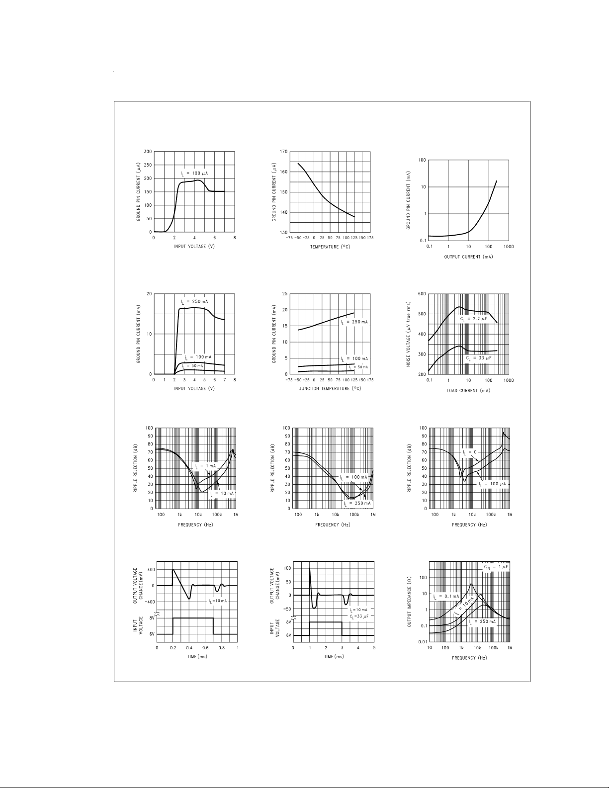
Typical Performance Characteristics Unless otherwise specified: V
=
3V, T
=
25˚C
A
Ground Pin Current
Ground Pin Current
vs Load
SD
Ground Pin Current
=
=
6V, I
L
1 mA, C
IN
=
L
2.2 µF, V
Ground Pin Current
Ripple Rejection
DS011340-19
DS011340-22
DS011340-25
Ground Pin Current
Ripple Rejection
DS011340-20
DS011340-23
DS011340-26
DS011340-21
Output Noise Voltage
DS011340-24
Ripple Rejection
DS011340-27
Line Transient Response
DS011340-28
Line Transient Response
www.national.com 4
DS011340-29
Output Impedance
DS011340-30
Page 5

Typical Performance Characteristics Unless otherwise specified: V
=
3V, T
A
=
25˚C (Continued)
V
SD
=
=
6V, I
IN
L
1 mA, C
L
=
2.2 µF,
Load Transient
Response
Enable Transient
DS011340-31
DS011340-34
Load Transient
Response
Enable Transient
DS011340-32
DS011340-35
Dropout
Characteristics
DS011340-33
Short-Circuit Output
Current and Maximum
Output Current
DS011340-36
Thermal Regulation
DS011340-37
Error Output
Sink Current
DS011340-38
Dropout Detection
Threshold Voltages
DS011340-39
www.national.com5
Page 6

Typical Performance Characteristics Unless otherwise specified: V
=
3V, T
A
=
25˚C (Continued)
V
SD
=
=
6V, I
IN
L
1 mA, C
L
=
2.2 µF,
Maximum Power Dissipation
(TO-263) (Note 2)
Block Diagram
DS011340-40
Error Output Voltage
DS011340-41
Dropout Voltage
DS011340-42
Typical Application Circuits
LP2957 Basic Application
www.national.com 6
DS011340-1
DS011340-2
Page 7

Typical Application Circuits (Continued)
LP2957 Application with Snap-On/Snap-Off Output
*See Application Hints
Application Hints
EXTERNAL CAPACITORS
A 2.2 µF (or greater) capacitor is required between the output pin and ground to assure stability (refer to
Without this capacitor, the part may oscillate. Most type of
tantalum or aluminum electrolytics will work here. Film types
will work, but are more expensive. Many aluminum electrolytics contain electrolytes which freeze at −30˚C, which requires the use of solid tantalums below −25˚C. The important
parameters of the capacitor are an ESR of about 5Ω or less
and a resonant frequency above 500 kHz (the ESR may increase by a factor of 20 or 30 as the temperature is reduced
from 25˚C to −30˚C). The value of this capacitor may be increased without limit. At lower values of output current, less
output capacitance is required for stability.The capacitor can
be reduced to 0.68 µF for currents below 10 mA or 0.22 µF
for currents below 1 mA.
A 1 µF capacitor should be placed from the input pin to
ground if there is more than 10 inches of wire between the input and the AC filter capacitor or if a battery input is used.
This capacitor may have to be increased if the regulator
is wired for snap-on/snap-off output and the source impedance is high (see
tion).
SHUTDOWN INPUT
A logic-level signal will shut off the regulator output when a
<
“LOW” (
To prevent possible mis-operation, the Shutdown input must
be actively terminated. If the input is driven from
open-collector logic, a pull-up resistor (20 kΩ to 100 kΩ recommended) must be connected from the Shutdown input to
the regulator input.
If the Shutdown input is driven from a source that actively
pulls high and low (like an op-amp), the pull-up resistor is not
required, but may be used.
If the shutdown function is not to be used, the cost of the
pull-up resistor can be saved by tying the Shutdown input directly to the regulator input.
IMPORTANT: Since the Absolute Maximum Ratings state
that the Shutdown input can not go more than 0.3V below
ground, the reverse-battery protection feature which protects
the regulator input is sacrificed if the Shutdown input is tied
directly to the regulator input.
If reverse-battery protection is required in an application, the
pull-up resistor between the Shutdown input and the regulator input must be used.
1.2V) is applied to the Shutdown input.
Snap-On/Snap-Off Operation
Figure 1
sec-
DS011340-4
MINIMUM LOAD
It should be noted that a minimum load current is specified in
several of the electrical characteristic test conditions, so the
).
value listed must be used to obtain correlation on these
tested limits. The part is parametrically tested down to
100 µA, but is functional with no load.
DROPOUT VOLTAGE
The dropout voltage of the regulator is defined as the minimum input-to-output voltage differential required for the output voltage to stay within 100 mV of the output voltage measured with a 1V differential. The dropout voltages for various
values of load current are listed under Electrical Characteristics.
If the regulator is powered from a transformer connected to
the AC line, the minimum AC line voltage and maximum
load current must be used to measure the minimum voltage
at the input of the regulator. The minimum input voltage is
the lowest voltage level including ripple on the filter ca-
pacitor . It is also advisable to verify operation at minimum
operating ambient temperature , since the increasing ESR
of the filter capacitor makes this a worst-case test due to increased ripple amplitude.
HEATSINK REQUIREMENTS
A heatsink may be required with the LP2957 depending on
the maximum power dissipation and maximum ambient temperature of the application. Under all possible operating conditions, the junction temperature must be within the range
specified under Absolute Maximum Ratings.
To determine if a heatsink is required, the maximum power
dissipated by the regulator, P(max), must be calculated. It is
important to remember that if the regulator is powered from
a transformer connected to the AC line, the maximum
specified AC input voltage must be used (since this produces the maximum DC input voltage to the regulator), and
the maximum load current must also be used.
shows the voltages and currents which are present in the circuit. The formula for calculating the power dissipated in the
regulator is also shown in
Figure 1
.
Figure 1
www.national.com7
Page 8

Application Hints (Continued)
Table 1
DS011340-7
and
Table
=
P
TOTAL
*See EXTERNAL CAPACITORS
− 5)IL+(VIN)I
(V
IN
G
FIGURE 1. Basic 5V Regulator Circuit
The next parameter which must be calculated is the maximum allowable temperature rise, T
by using the formula:
T
(Max)=TJ(Max) − TA(Max)
R
where: T
(Max) is the maximum allowable junction tem-
J
perature
T
(Max) is the maximum ambient temperature
A
Using the calculated values for T
quired value for junction-to-ambient thermal resistance, θ
(JA)
, can now be found:
=
(JA)
(Max)/P(Max)
T
R
θ
(Max). This is calculated
R
(Max) and P(Max), the re-
R
If the calculated value is 60˚C/W or higher , the regulator
may be operated without an external heatsink. If the calculated value is below 60˚C/W, an external heatsink is required. The required thermal resistance for this heatsink,
θ
, can be calculated using the formula:
(HA)
=
− θ
θ
θ
(HA)
(JA)
(JC)
− θ
(CH)
where:
is the junction-to-case thermal resistance, which is
θ
(JC)
specified as 3˚C/W for the LP2957.
θ
is the case-to-heatsink thermal resistance, which is de-
(CH)
pendent on the interfacing material (see
2
).
Typical TO-220 Case-To-Heatsink
Thermal Resistance in ˚C/W
TABLE 1. (From AAVID)
Silicone Grease 1.0
Dry Interface 1.3
Mica with Grease 1.4
TABLE 2. (From Thermalloy)
Thermasil III 1.3
Thermasil II 1.5
Thermalfilm (0.002) 2.2
with Grease
θ
is the heatsink-to-ambient thermal resistance. It is this
(HA)
specification (listed on the heatsink manufacturers data
sheet) which defines the effectiveness of the heatsink. The
heatsink selected must have a thermal resistance which is
equal to or lower than the value of θ
above listed formula.
calculated from the
(HA)
ERROR COMPARATOR
This comparator produces a logic “LOW” whenever the output falls out of regulation by more than about 5%. This figure
results from the comparator’s built-in offset of 60 mV divided
by the 1.23V reference. An out-of-regulation condition can
result from low input voltage, current limiting, or thermal limiting.
Figure 2
gives a timing diagram showing the relationship between the output voltage, the ERROR output, and input voltage as the input voltage is ramped up and down to the regulator without snap-on/snap-off output. The ERROR signal
becomes low at about 1.3V input. It goes high at about 5V input, where the output equals 4.75V. Since the dropout voltage is load dependent, the input voltage trip points will vary
with load current. The output voltage trip point does not
vary.
The comparator has an open-collector output which requires
an external pull-up resistor. This resistor may be connected
to the regulator output or some other supply voltage. Using
the regulator output prevents an invalid “HIGH” on the comparator output which occurs if it is pulled up to an external
voltage while the regulator input voltage is reduced below
1.3V. In selecting a value for the pull-up resistor, note that
while the output can sink 400 µA, this current adds to battery
drain. Suggested values range from 100k to 1 MΩ. The resistor is not required if the output is unused.
www.national.com 8
Page 9

Application Hints (Continued)
*
In shutdown mode, ERROR will go high if it has been pulled up to an
external supply. To avoid this invalid response, pull up to regulator output.
*
Exact value depends on dropout voltage, which varies with load current.
*
FIGURE 2. ERROR Output Timing
If a single pull-up resistor is connected to the regulator output, the error flag may briefly rise up to about 1.3V as the input voltage ramps up or down through the 0V to 1.3V region.
In some cases, this 1.3V signal may be mis-interpreted as a
false high by a µP which is still “alive” with 1.3V applied to it.
To prevent this, the user may elect to use two resistors
which are equal in value on the error output (one connected
to ground and the other connected to the regulator output).
If this two-resistor divider is used, the error output will only be
pulled up to about 0.6V (not 1.3V) during power-up or
power-down, so it can not be interpreted as a high signal.
When the regulator output is in regulation (4.8V to 5V), the
error output voltage will be 2.4V to 2.5V, which is clearly a
high signal.
OUTPUT ISOLATION
The regulator output can be connected to an active voltage
source (such as a battery) with the regulator input turned off,
as long as the regulator ground pin is connected to
ground . If the ground pin is left floating, damage to the
regulator can occur if the output is pulled up by an external
voltage source.
SNAP-ON/SNAP-OFF OPERATION
The LP2957 output can be wired for snap-on/snap-off operation using three external resistors:
DS011340-14
DS011340-9
FIGURE 4. Snap-On/Snap-Off Input
and Output Voltage Diagram
It is important to note that the voltage V
lower than V
called the hysteresis).
(the difference in these voltage levels is
ON
must always be
OFF
Hysteresis is required when using snap-on/snap-off output,
with the minimum amount of hysteresis required for a specific application being dependent on the source impedance
of whatever is supplying V
.
IN
Caution: A type of low-frequency oscillation can occur if
V
and V
ON
hysteresis ). When the output snaps on, the regu-
are too close together (insufficient
OFF
lator must draw sufficient current to power the
load and charge up the output capacitor (in most
cases, the regulator will briefly draw the maximum
current allowed by its internal limiter).
For this reason, it is best to assume the LP2957
may pull a peak current of about 600 mA from the
source (which is the listed maximum short-circuit
load current of 530 mA plus the ground pin current
of 70 mA ).
This high peak current causes V
equal to the source impedance multiplied by the current. If V
IN
drops below V
ing current from the source. This will allow V
above V
ON
stay in this oscillating mode and never come into regulation.
, the regulator will turn off and stop draw-
OFF
, and the cycle will start over. The regulator will
to drop by an amount
IN
to rise back up
IN
HYSTERESIS IN TRANSFORMER-POWERED
APPLICATIONS:
If the unregulated DC input voltage to the regulator comes
from a transformer, the required hysteresis is easily measured by loading the source with a resistive load.
*Minimum value (increase as required for smooth turn-on characteristic).
DS011340-8
FIGURE 3. Snap-On/Snap-Off Output
When connected as shown, the shutdown input holds the
regulator off until the input voltage rises up to the turn-on
threshold (V
), at which point the output “snaps on”.
ON
When the input power is shut off (and the input voltage starts
to decay) the output voltage will snap off when the input voltage reaches the turn-off threshold, V
OFF
.
DS011340-10
FIGURE 5. Transformer Powered Input Supply
If the regulator is powered from a battery, the source impedance will probably be low enough that other considerations
will determine the optimum values for hysteresis (see Design
#
Example
2).
For best results, the load resistance used to test the transformer should be selected to draw about 600 mA for the
maximum load current test, since this is the maximum peak
current the LP2957 could be expected to draw from the
source.
www.national.com9
Page 10

Application Hints (Continued)
The difference in input voltage measured at no load and
full load defines the amount of hysteresis required for
proper snap-on/snap-off operation (the programmed hys-
teresis must be greater than the difference in voltages).
CALCULATING RESISTOR VALUES:
The values of R1, R2 and R3 can be calculated assuming
the designer knows the hysteresis.
In most transformer-powered applications, it can be as-
sumed that V
for about 5.5V, since this allows about 500 mV across the
LP2957 to keep the output in regulation until it snaps off. V
(the input voltage at turn on) is found by adding the hyster-
esis voltage to V
R1, R2 and R3 are found by solving the node equations for
the currents entering the node nearest the shutdown pin
(written at the turn-on and turn-off thresholds).
The shutdown pin bias current (10 nA typical) is not included
in the calculations:
(the input voltage at turn-off) should be set
OFF
.
OFF
Turn-ON Transition
DS011340-11
Turn-OFF Transition
ON
Setting these equal to each other and solving for R1 yields:
The same equation solved for R3 is:
A value for R1 or R3 can be derived using either one of the
above equations, if the designer assumes a value for one of
the resistors.
The simplest approach is to assume a value for R3. Best results will typically be obtained using values between about
20 kΩ and 100 kΩ (this keeps the current drain low, but also
generates realistic values for the other resistors).
There is no limit on the minimum value of R3, but current
should be minimized as it generates power that drains the
source and does not power the load.
SUMMARY: TO SOLVE FOR R1, R2 AND R3:
1. Assume a value for either R1 or R3.
2. Solve for the other variable using the equation for R1 or
R3.
3. Take the values for R1 and R3 and plug them back into
either equation for R2 and solve for this value.
DESIGN EXAMPLE
#
1:
A 5V regulated output is to be powered from a transformer
secondary which is rectified and filtered. The voltage V
measured at zero current and maximum current (600 mA) to
IN
determine the minimum allowable hysteresis.
V
is measured using an oscilloscope (both traces are
IN
shown on the same grid for clarity):
is
DS011340-12
FIGURE 6. Equivalent Circuits
Since these two equations contain three unknowns (R1, R2
and R3) one resistor value must be assumed and then the
remaining two values can be obtained by solving the equations.
The node equations will be simplified by solving both equations for R2, and then equating the two to generate an expression in terms of R1 and R3.
www.national.com 10
DS011340-13
FIGURE 7. VINVOLTAGE WAVEFORMS
The full-load voltage waveform from a transformer-powered
supply will have ripple voltage as shown. The correct point to
measure is the lowest value of the waveform.
The 1.2V differential between no-load and full-load conditions means that at least 1.2V of hysteresis is required for
proper snap-on/snap-off operation (for this example, we will
use 1.5V ).
As a starting point, we will assume:
=
5.5V
V
OFF
=
+ HYST=5.5 + 1.5=7V
V
V
ON
OFF
R3=49.9k
Solving for R1:
Page 11

Application Hints (Continued)
Solving for R2:
DESIGN EXAMPLE#2:
A 5V regulated output is to be powered from a battery made
up of six NiCad cells. The cell data is:
cell voltage (full charged): 1.4V
cell voltage (90%discharged): 1.0V
The internal impedance of a typical battery is low enough
that source loading during regulator turn-on is not usually a
problem.
In a battery-powered application, the turn-off voltage V
should be selected so that the regulator is shut down when
the batteries are about 90%discharged (over discharge can
damage rechargeable batteries).
In this case, the battery voltage will be 6.0V at the 90%discharge point (since there are six cells at 1.0V each). That
means for this application, V
Selecting the optimum voltage for V
ing battery behavior. If a Ni-Cad battery is nearly discharged
will be set to 6.0V.
OFF
requires understand-
ON
OFF
(cell voltage 1.0V) and the load is removed , the cell voltage will drift back up. The voltage where the regulator turns
on must be set high enough to keep the regulator from
re-starting during this time, or an on-offpulsing mode can occur.
If the regulator restarts when the discharged cell voltage
drifts up, the load on the battery will cause the cell voltage to
fall below the turn-off level, which causes the regulator to
shut down. The cell voltage will again float up and the on-off
cycling will continue.
For NiCad batteries, a good cell voltage to use to calculate
V
is about 1.2V per cell. In this application, this will yield a
ON
value for V
ON
of 7.2V.
We can now find R1, R2 and R3 assuming:
=
6.0V V
V
OFF
=
7.2V R3=49.9k
ON
Solving for R1:
Solving for R2:
www.national.com11
Page 12

Schematic Diagram
DS011340-15
www.national.com 12
Page 13

Physical Dimensions inches (millimeters) unless otherwise noted
Bent, Staggered 5-Lead TO-220 (T)
Order Number LP2957AIT or LP2957IT
NS Package Number T05D
www.national.com13
Page 14

Physical Dimensions inches (millimeters) unless otherwise noted (Continued)
TO-263 5-Lead Plastic Surface Mount Package
Order Number LP2957AIS or LP2957IS
NS Package Number TS5B
LP2957/LP2957A 5V Low-Dropout Regulator for µP Applications
LIFE SUPPORT POLICY
NATIONAL’S PRODUCTS ARE NOT AUTHORIZED FOR USE AS CRITICAL COMPONENTS IN LIFE SUPPORT
DEVICES OR SYSTEMS WITHOUT THE EXPRESS WRITTEN APPROVAL OF THE PRESIDENT AND GENERAL
COUNSEL OF NATIONAL SEMICONDUCTOR CORPORATION. As used herein:
1. Life support devices or systems are devices or
systems which, (a) are intended for surgical implant
into the body, or (b) support or sustain life, and
whose failure to perform when properly used in
accordance with instructions for use provided in the
labeling, can be reasonably expected to result in a
significant injury to the user.
National Semiconductor
Corporation
Americas
Tel: 1-800-272-9959
Fax: 1-800-737-7018
Email: support@nsc.com
www.national.com
National does not assume any responsibility for use of any circuitry described, no circuit patent licenses are implied and National reserves the right at any time without notice to change said circuitry and specifications.
National Semiconductor
Europe
Fax: +49 (0) 1 80-530 85 86
Email: europe.support@nsc.com
Deutsch Tel: +49 (0) 1 80-530 85 85
English Tel: +49 (0) 1 80-532 78 32
Français Tel: +49 (0) 1 80-532 93 58
Italiano Tel: +49 (0) 1 80-534 16 80
2. A critical component is any component of a life
support device or system whose failure to perform
can be reasonably expected to cause the failure of
the life support device or system, or to affect its
safety or effectiveness.
National Semiconductor
Asia Pacific Customer
Response Group
Tel: 65-2544466
Fax: 65-2504466
Email: sea.support@nsc.com
National Semiconductor
Japan Ltd.
Tel: 81-3-5639-7560
Fax: 81-3-5639-7507
 Loading...