

Page 1
LP2956/LP2956A
Dual Micropower Low-Dropout Voltage Regulators
General Description
The LP2956 is a micropower voltage regulator with very low
quiescent current (170 µAtypical at light loads) and very low
dropout voltage (typically 60 mV at 1 mA load current and
470 mV at 250 mA load current on the main output).
The LP2956 retains all the desirable characteristics of the
LP2951, but offers increased output current (main output),
an auxiliary LDO adjustable regulated output (75 mA), and
additional features.
The auxiliary output is always on (regardless of main output
status), so it can be used to power memory circuits.
Quiescent current increases only slightly at dropout, which
prolongs battery life.
The error flag goes low if the main output voltage drops out
of regulation.
An open-collector auxiliary comparator is included, whose inverting input is tied to the 1.23V reference.
Reverse battery protection is provided.
The parts are available in DIP and surface mount packages.
Features
n Output voltage adjusts from 1.23V to 29V
n Guaranteed 250 mA current (main output)
n Auxiliary LDO (75 mA) adjustable output
n Auxiliary comparator with open-collector output
n Shutdown pin for main output
n Extremely low quiescent current
n Low dropout voltage
n Extremely tight line and load regulation
n Very low temperature coefficient
n Current and thermal limiting
n Reverse battery protection
Applications
n High-efficiency linear regulator
n Low dropout battery-powered regulator
n µP system regulator with switchable high-current V
CC
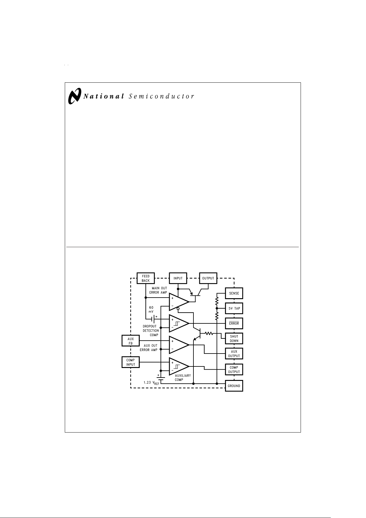
Block Diagram
LP2956
DS011339-1
May 1999
LP2956/LP2956A Dual Micropower Low-Dropout Voltage Regulators
© 1999 National Semiconductor Corporation DS011339 www.national.com
Page 2
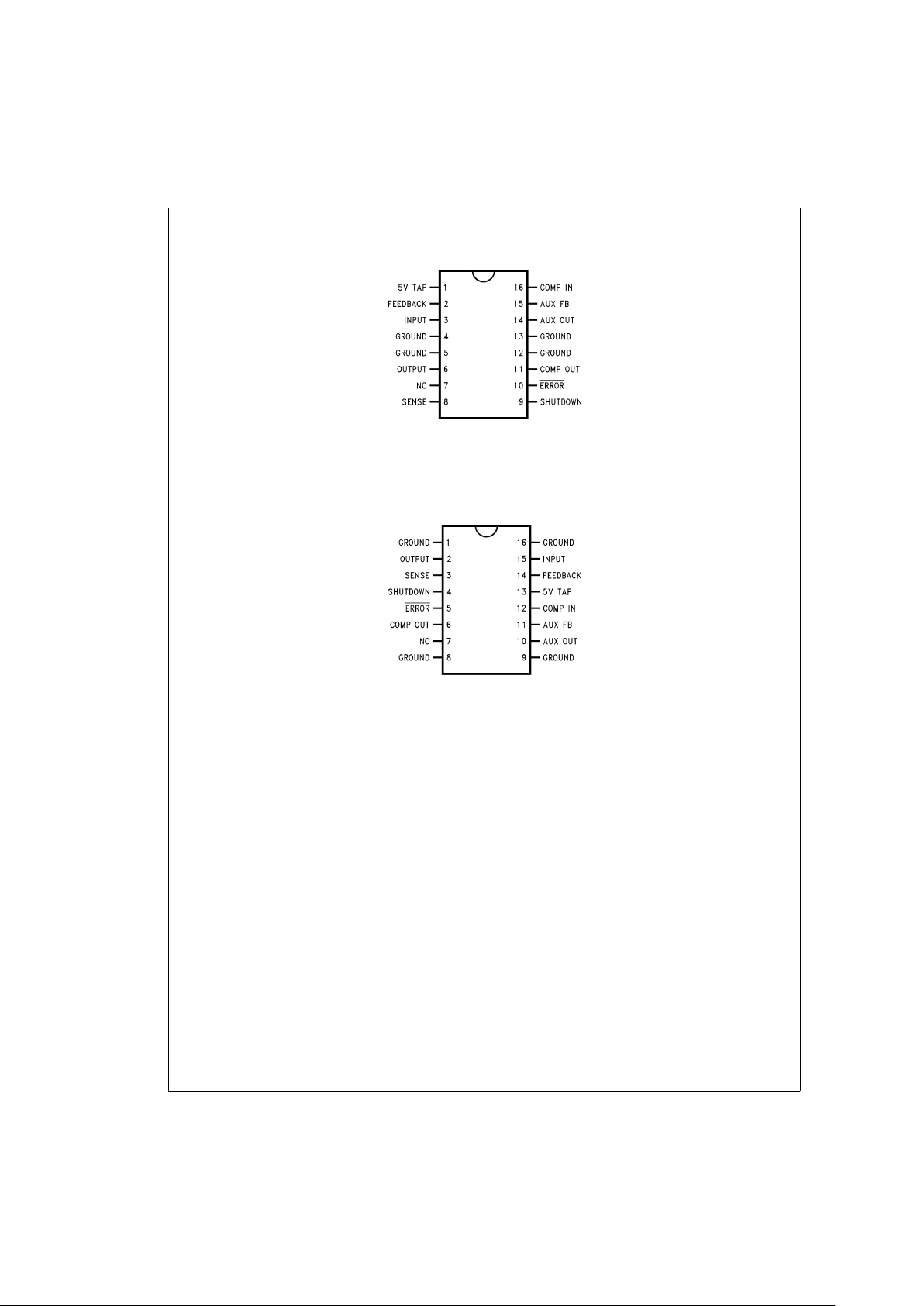
Connection Diagrams
16–Pin DIP
DS011339-2
Order Number LP2956IN or LP2956AIN
See NS Package Number N16A
Order Number LP2956AMJ-QML or 5962-9554701QEA
See NS Package Number J16A
16-Pin Surface Mount
DS011339-3
Order Number LP2956IM or LP2956AIM
See NS Package Number M16A
www.national.com 2
Page 3
Absolute Maximum Ratings (Note 1)
If Military/Aerospace specified devices are required,
please contact the National Semiconductor Sales Office/
Distributors for availability and specifications.
Storage Temperature Range −65˚C to +150˚C
Operating Junction
Temperature Range −40˚C to +125˚C
Lead Temperature
(Soldering, 5 seconds) 260˚C
Power Dissipation (Note 2) Internally Limited
Input Supply Voltage −20V to +30V
Feedback Input Voltage (Note 3) −0.3V to +5V
Aux. Feedback Input Voltage (Note 3) −0.3V to +5V
Shutdown Input Voltage (Note 3) −0.3V to +30V
Comparator Input Voltage (Notes 3,
4) −0.3V to +30V
Comparator Output Voltage (Notes 3,
4) −0.3V to +30V
ESD Rating (Note 16) 2 kV
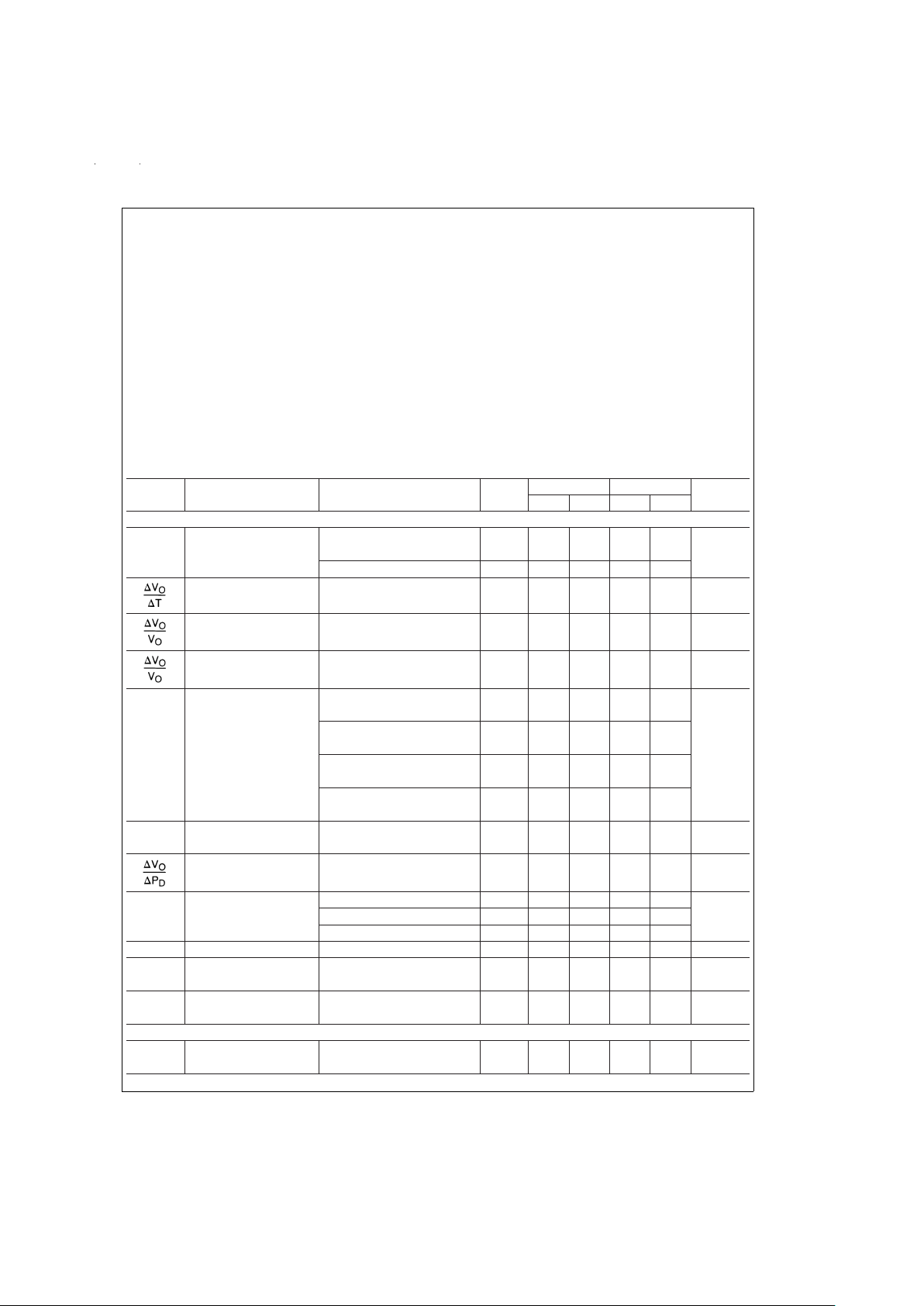
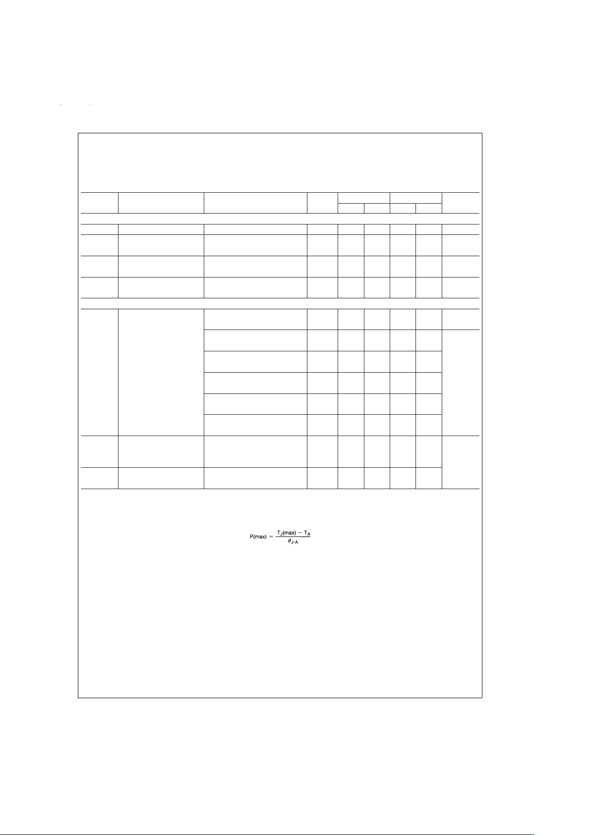
Electrical Characteristics
Limits in standard typeface are for T
J
=
25˚C, and limits in boldface type apply over the full operating temperature range. Limits are guaranteed by production testing or correlation techniques using standard Statistical Quality Control (SQC) methods.
Unless otherwise specified: V
IN
=
6V, C
L
=
2.2 µF (Main Output) and 10 µF (Auxiliary Output), Feedback pin is tied to 5V Tap
pin, C
IN
=
1 µF, V
SD
=
0V, Main Output pin is tied to Output Sense pin, Auxiliary Output is programmed for 5V. The main
regulator output hasa1mAload, the auxiliary regulator output has a 100 µA load.
Symbol Parameter Conditions Typical LP2956AI LP2956I Units
Min Max Min Max
MAIN OUTPUT
V
O
Output Voltage 5.0 4.975 5.025 4.950 5.050
4.940 5.060 4.900 5.100 V
1mA≤I
L
≤250 mA 5.0 4.930 5.070 4.880 5.120
Temperature Coefficient (Note 5) 20 100 150 ppm/˚C
Line Regulation V
IN
=
6V to 30V 0.03 0.1 0.2
%
0.2 0.4
Load Regulation I
L
=
1 mA to 250 mA 0.04 0.16 0.20
%
I
L
=
0.1 mA to 1 mA (Note 6) 0.20 0.30
V
IN–VO
Dropout Voltage I
L
=
1 mA 60 100 100
(Note 7) 150 150
I
L
=
50 mA 240 300 300
420 420 mV
I
L
=
100 mA 310 400 400
520 520
I
L
=
250 mA 470 600 600
800 800
I
LIMIT
Current Limit R
L
=
1Ω 380 500 500 mA
530 530
Thermal Regulation (Note 8) 0.05 0.2 0.2
%
/W
e
n
Output Noise Voltage C
L
=
2.2 µF 400
(10 Hz to 100 KHz) C
L
=
33 µF 260 µV RMS
I
L
=
100 mA C
L
=
33 µF (Note 9) 80
V
FB
Feedback Pin Voltage 1.23 1.215 1.245 1.205 1.255 V
I
FB
Feedback Pin Bias 20 40 40 nA
Current 60 60
I
O
Output Leakage I
(SD IN)
≥ 1 µA 3 10 10 µA
(OFF) In Shutdown V
IN
=
30V, V
OUT
=
0V 20 20
AUXILIARY OUTPUT
V
FB
Feedback Pin Voltage 1.23 1.22 1.25 1.21 1.26 V
1.21 1.26 1.20 1.27
www.national.com3
Page 4
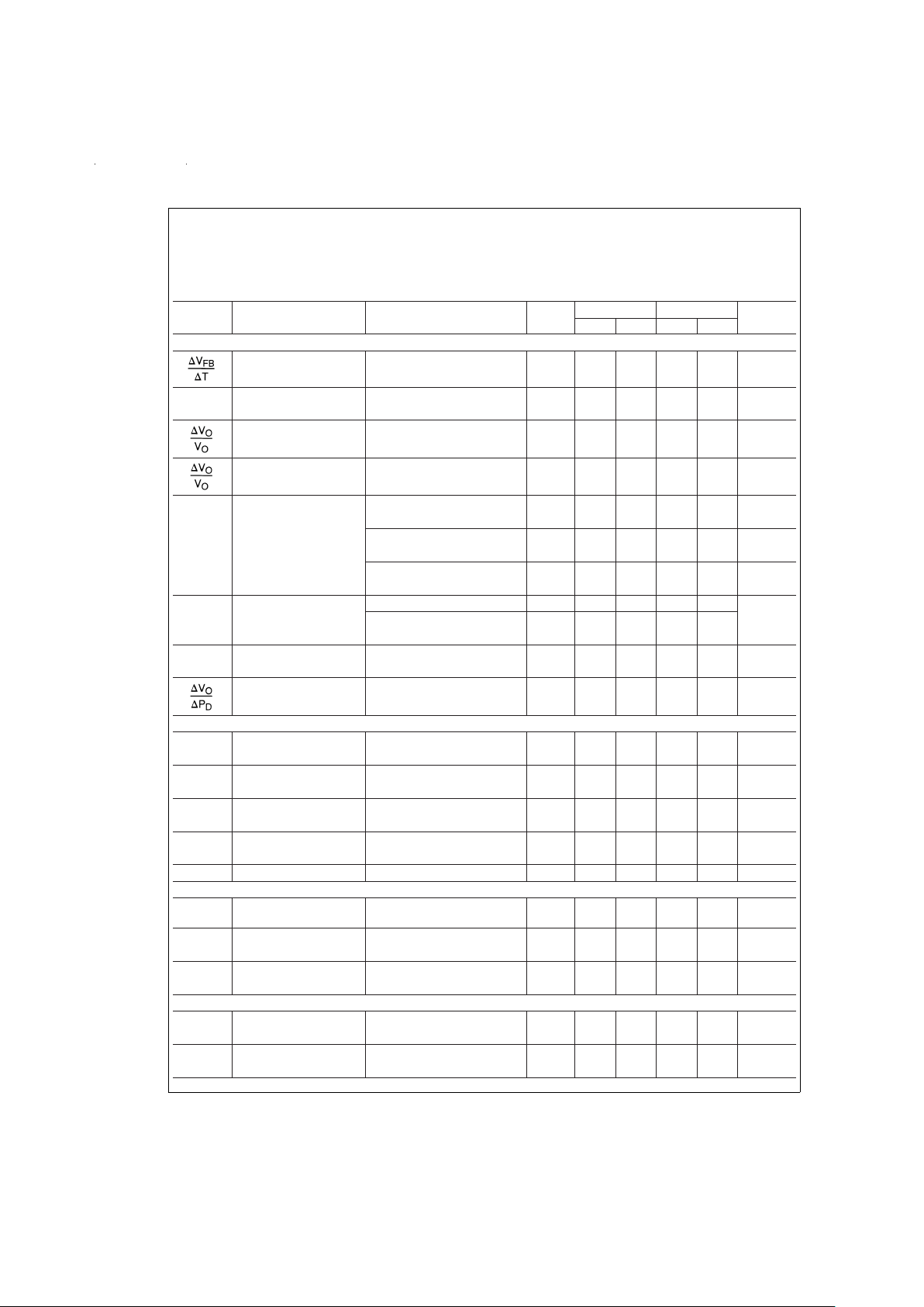
Electrical Characteristics (Continued)
Limits in standard typeface are for T
J
=
25˚C, and limits in boldface type apply over the full operating temperature range. Limits are guaranteed by production testing or correlation techniques using standard Statistical Quality Control (SQC) methods.
Unless otherwise specified: V
IN
=
6V, C
L
=
2.2 µF (Main Output) and 10 µF (Auxiliary Output), Feedback pin is tied to 5V Tap
pin, C
IN
=
1 µF, V
SD
=
0V, Main Output pin is tied to Output Sense pin, Auxiliary Output is programmed for 5V. The main
regulator output hasa1mAload, the auxiliary regulator output has a 100 µA load.
Symbol Parameter Conditions Typical LP2956AI LP2956I Units
Min Max Min Max
AUXILIARY OUTPUT
Feedback Voltage
Temperature Coefficient
20 ppm/˚C
I
FB
Feedback Pin Bias 10 20 20 nA
Current 30 30
Line Regulation 6V ≤ VIN≤ 30V 0.07 0.3 0.4
%
0.5 0.6
Load Regulation I
L
=
0.1 mA to 1 mA 0.1 0.3 0.4
%
I
L
=
1 mA to 75 mA (Note 10) 0.6 1.0
V
IN–VO
Dropout Voltage I
L
=
1 mA 100 200 200 mV
300 300
I
L
=
50 mA 400 600 600 mV
700 700
I
L
=
75 mA 500 700 700 mV
850 850
e
n
Output Noise C
L
=
10 µF 300
(10 Hz–100 KHz) C
L
=
33 µF (Note 9) 100 µV RMS
I
L
=
10 mA
I
LIM
Current Limit V
OUT
=
0V (Note 13) 80 200 200 mA
250 250
Thermal Regulation (Note 8) 0.2 0.5 0.5
%
/W
DROPOUT DETECTION COMPARATOR
I
OH
Output “HIGH” Leakage V
OH
=
30V 0.01 1 1 µA
22
V
OL
Output “LOW” Voltage V
IN
=
4V 150 250 250 mV
I
O
(COMP)=400 µA 400 400
V
THR
Upper Threshold Voltage (Note 11) −240 −320 −150 −320 −150 mV
(max) −380 −100 −380 −100
V
THR
Lower Threshold Voltage (Note 11) −350 −450 −230 −450 −230 mV
(min) −640 −160 −640 −160
HYST Hysteresis (Note 11) 110 mV
SHUTDOWN INPUT
I
IN
Input Current to Disable
Output
(Note 12) 0.03 0.5 0.5 µA
V
IH
Shutdown Input High I
(SD IN)
≥ 1 µA 900 900 mV
Threshold 1200 1200
V
IL
Shutdown Input Low VO≥ 4.5V 400 400 mV
Threshold 200 200
AUXILIARY COMPARATOR
V
T
(high) Upper Trip Point (Note 14) 1.236 1.20 1.28 1.20 1.28 V
1.19 1.29 1.19 1.29
V
T
(low) Lower Trip Point (Note 14) 1.230 1.19 1.27 1.19 1.27 V
1.18 1.28 1.18 1.28
www.national.com 4
Page 5
Electrical Characteristics (Continued)
Limits in standard typeface are for T
J
=
25˚C, and limits in boldface type apply over the full operating temperature range. Limits are guaranteed by production testing or correlation techniques using standard Statistical Quality Control (SQC) methods.
Unless otherwise specified: V
IN
=
6V, C
L
=
2.2 µF (Main Output) and 10 µF (Auxiliary Output), Feedback pin is tied to 5V Tap
pin, C
IN
=
1 µF, V
SD
=
0V, Main Output pin is tied to Output Sense pin, Auxiliary Output is programmed for 5V. The main
regulator output hasa1mAload, the auxiliary regulator output has a 100 µA load.
Symbol Parameter Conditions Typical LP2956AI LP2956I Units
Min Max Min Max
AUXILIARY COMPARATOR
HYST Hysteresis 6 mV
I
OH
Output “HIGH” Leakage V
OH
=
30V 0.01 1 1 µA
V
IN
(COMP)=1.3V 22
V
OL
Output “LOW” Voltage VIN(COMP)=1.1V 150 250 250 mV
I
O
(COMP)=400 µA 400 400
I
B
Input Bias Current 0 ≤ VIN(COMP) ≤ 5V 10 −30 30 −30 30 nA
−50 50 −50 50
GROUND PIN CURRENT
I
GND
Ground Pin Current IL(Main Out)=1 mA 170 250 250 µA
(Note 15) I
L
(Aux. Out)=0.1 mA 280 280
I
L
(Main Out)=50 mA 1.1 2 2
I
L
(Aux. Out)=1mA 2.5 2.5
I
L
(Main Out)=100 mA 3 6 6
I
L
(Aux. Out)=1mA 88
I
L
(Main Out)=250 mA 16 28 28 mA
I
L
(Aux. Out)=1mA 33 33
I
L
(Main Out)=1mA 3 6 6
I
L
(Aux. Out)=50 mA 88
I
L
(Main Out)=1mA 6 8 8
I
L
(Aux. Out)=75 mA 10 10
I
GND
Ground Pin Current V
IN
=
4.5V 325 325
at Dropout (Note 15) I
L
(Main Out)=0.1 mA 270 350 350
I
L
(Aux. Out)=0.1 mA µA
I
GND
Ground Pin Current No Load on Either Output 120 180 180
at Shutdown (Note 15) I
(SD IN
) ≥ 1µA 200 200
Note 1: Absolute maximum ratings indicate limits beyond which damage to the component may occur. Electrical specifications do not apply when operating the device outside of its rated operating conditions.
Note 2: The maximum allowable power dissipation is a function of the maximum junction temperature, T
J
(max), the junction-to-ambient thermal resistance, θ
J-A
,
and the ambient temperature, T
A
. The maximum allowable power dissipation at any ambient temperature is calculated using: P(max)
=
.
Exceeding the maximum allowable power dissipation will cause excessive die temperature, and the regulator will go into thermal shutdown. SeeApplication Hints for
additional information on heat sinking and thermal resistance.
Note 3: When used in dual-supply systems where the regulator load is returned to a negative supply, the output voltage must be diode-clamped to ground.
Note 4: May exceed the input supply voltage.
Note 5: Output or reference voltage temperature coefficient is defined as the worst case voltage change divided by the total temperature range.
Note 6: Load regulation is measured at constant junction temperature using low duty cycle pulse testing. Twoseparate tests are performed, one for the range of 100
µA to 1 mA and one for the 1 mA to 250 mA range. Changes in output voltage due to heating effects are covered by the thermal regulation specification.
Note 7: Dropout voltage is defined as the input to output differential at which the output voltage drops 100 mV below the value measured with a 1V differential. At
very low values of programmed output voltage, the input voltage minimum of 2V (2.3V over temperature) must be observed.
Note 8: Thermal regulation is the change in output voltage at a time T after a change in power dissipation, excluding load or line regulation effects. Specifications
are for a 200 mA load pulse at V
IN
=
20V (3W pulse) for T=10 ms on the Main regulator output. For the Auxiliary regulator output, specifications are for a 66 mA
load pulse at V
IN
=
20V (1W pulse) for T=10 ms.
Note 9: Connect a 0.1 µF capacitor from the output to the feedback pin.
Note 10: Load regulation is measured at constant junction temperature using low duty cycle pulse testing. Two separate tests are performed, one for the range of
100 µA to 1 mA and one for the 1 mA to 75 mA range. Changes in output voltage due to heating effects are covered by the thermal regulation specification.
Note 11: Dropout dectection comparator thresholds are expressed as changes in a 5V output. To express the threshold voltages in terms of a differential at the
Feedback terminal, divide by the error amplifier gain=V
OUT/VREF
.
www.national.com5
Page 6

Electrical Characteristics (Continued)
Note 12: The shutdown input equivalent circuit is the base of a grounded-emitter NPN transistor in series with a current-limiting resistor. Pulling the shutdown input
high turns off the main regulator. For more details, see Application Hints.
Note 13: The auxiliary regulator output has foldback limiting, which means the output current reduces with output voltage. The tested limit is for V
OUT
=
0V,so the
output current will be higher at higher output voltages.
Note 14: This test is performed with the auxiliary comparator output sinking 400 µA of current. At the upper trip point, the comparator output must be ≥2.4V. At the
low trip point, the comparator output must be ≤ 0.4V.
Note 15: Ground pin current is the regulator quiescent current. The total current drawn from the source is the sum of the ground pin current, output load current, and
current through the external resistive dividers (if used).
Note 16: All pins are rated for 2 kV, except for the auxiliary feedback pin which is rated for 1.2 kV (human body model, 100 pF discharged through 1.5 kΩ).
Typical Performance Characteristics Unless otherwise specified: V
IN
=6V,CL= 2.2 µF (Main Out-
put) and 10 µF (Auxiliary Output), Feedback is tied to 5V Tap pin, C
IN
=1µF,VSD= 0V, Main Output pin is tied to Output
Sense pin, Auxiliary Output is programmed for 5V. The main regulator output hasa1mAload, the auxiliary output has a
100 µA load.
Ground Pin Current
DS011339-18
Ground Pin Current
DS011339-19
Ground Pin Current
DS011339-20
Ground Pin Current
DS011339-21
Ground Pin Current
DS011339-22
Ground Pin Current
DS011339-23
Ground Pin Current
vs Main Load
DS011339-24
Dropout Characteristics
(Main Regulator)
DS011339-25
Dropout Voltage vs
Temperature (Main Regulator)
DS011339-26
www.national.com 6
Page 7

Typical Performance Characteristics Unless otherwise specified: V
IN
= 6V, CL= 2.2 µF (Main
Output) and 10 µF (Auxiliary Output), Feedback is tied to 5V Tap pin, C
IN
= 1 µF, VSD= 0V, Main Output pin is tied to Output
Sense pin, Auxiliary Output is programmed for 5V. The main regulator output hasa1mAload, the auxiliary output has a
100 µA load. (Continued)
Current Limit vs Regulator
(Main Regulator)
DS011339-27
Enable Transient
(Main Regulator)
DS011339-28
Enable Transient
(Main Regulator)
DS011339-29
Load Transient Response
(Main Regulator)
DS011339-30
Load Transient Response
(Main Regulator)
DS011339-31
Line Transient Response
(Main Regulator)
DS011339-32
Line Transient Response
(Main Regulator)
DS011339-33
Ripple Rejection
(Main Regulator)
DS011339-34
Ripple Rejection
(Main Regulator)
DS011339-35
www.national.com7
Page 8

Typical Performance Characteristics Unless otherwise specified: V
IN
= 6V, CL= 2.2 µF (Main
Output) and 10 µF (Auxiliary Output), Feedback is tied to 5V Tap pin, C
IN
= 1 µF, VSD= 0V, Main Output pin is tied to Output
Sense pin, Auxiliary Output is programmed for 5V. The main regulator output hasa1mAload, the auxiliary output has a
100 µA load. (Continued)
Ripple Rejection
(Main Regulator)
DS011339-36
Thermal Regulation
(Main Regulator)
DS011339-37
Output Impedance
(Main Regulator)
DS011339-38
Output Noise Voltage
(Main Regulator)
DS011339-39
Feedback Bias Current
DS011339-40
Divider Resistance
DS011339-41
Dropout Characteristics
(Auxiliary Regulator)
DS011339-42
Dropout vs Temperature
(Auxiliary Regulator)
DS011339-43
Current Limit vs Temperature
(Auxiliary Regulator)
DS011339-44
www.national.com 8
Page 9

Typical Performance Characteristics Unless otherwise specified: V
IN
= 6V, CL= 2.2 µF (Main
Output) and 10 µF (Auxiliary Output), Feedback is tied to 5V Tap pin, C
IN
= 1 µF, VSD= 0V, Main Output pin is tied to Output
Sense pin, Auxiliary Output is programmed for 5V. The main regulator output hasa1mAload, the auxiliary output has a
100 µA load. (Continued)
Line Transient Response
(Auxiliary Regulator)
DS011339-45
Load Transient Response
(Auxiliary Regulator)
DS011339-46
Load Transient Response
(Auxiliary Regulator)
DS011339-47
Ripple Rejection
(Auxiliary Regulator)
DS011339-48
Output Impedance
(Auxiliary Regulator)
DS011339-49
Output Noise Voltage
(Auxiliary Regulator)
DS011339-50
Auxiliary Comparator
Sink Current
DS011339-51
Error Output Voltage
DS011339-52
Dropout Detection Comparator
Threshold Voltages
DS011339-53
www.national.com9
Page 10

Application Hints
HEATSINK REQUIREMENTS
A heatsink may be required with the LP2956 depending on
the maximum power dissipation and maximum ambient temperature of the application. Under all expected operating
conditions, the junction temperature must be within the
range specified under Absolute Maximum Ratings.
To determine if a heatsink is required, the maximum power
dissipated by the regulator, P(max), must be calculated. It is
important to remember that if the regulator is powered from
a transformer connected to the AC line, the maximum
specified AC input voltage must be used (since this produces the maximum DC input voltage to the regulator).
Fig-
ure 1
shows the voltages and currents which are present in
the circuit. The formula for calculating the power dissipated
in the regulator is also shown in
Figure 1
(the currents and
power due to external resistive dividers are not included, and
are typically negligible).
The next parameter which must be calculated is the maximum allowable temperature rise, T
R
(max). This is calculated
by using the formula:
T
R
(max)=TJ(max) − TA(max)
where: T
J
(max) is the maximum allowable junction tem-
perature
T
A
(max) is the maximum ambient temperature
Using the calculated values for T
R
(max) and P(max), the re-
quired value for junction-to-ambient thermal resistance, θ
(J-A)
, can now be found:
θ
(J-A)
=
T
R
(max)/P(max)
The heatsink for the LP2956 is made using the PC board
copper.The heat is conducted from the die, through the lead
frame (inside the part), and out the pins which are soldered
to the PC board. The pins used for heat conduction are
shown in
Table 1
.
TABLE 1.
Part Package Pins
LP2956IN 16-Pin Plastic DIP 4, 5, 12, 13
LP2956AIN 16-Pin Plastic DIP 4, 5, 12, 13
LP2956IM 16-Pin Surface Mt. 1, 8, 9, 16
LP2956AIM 16-Pin Surface Mt. 1, 8, 9, 16
Figure 2
shows copper patterns which may be used to dissi-
pate heat from the LP2956:
Table 2
shows some typical values of junction-to-ambient
thermal resistance (θ
J-A
) for values of L and W (1 oz. cop-
per).
TABLE 2.
Package L (In.) H (In.) θ
J-A
(˚C/W)
16-Pin
Plastic
1 0.5 70
DIP 2 1 60
3 1.5 58
4 0.19 66
6 0.19 66
16-Pin 1 0.5 83
Surface 2 1 70
Mount 3 1.5 67
6 0.19 69
4 0.19 71
2 0.19 73
EXTERNAL CAPACITORS
A 2.2 µF (or greater) capacitor is required between the main
output pin and ground to assure stability. The auxiliary output
requires 10 µF to ground. Without these capacitors, the part
may oscillate. Most types of tantalum or aluminum electrolytics will work here. Film types will work, but are more expensive. Many aluminum electrolytics contain electrolytes which
freeze at −30˚C, which requires the use of solid tantalums
below −25˚C. The important characteristic of the capacitors
is an ESR of 5Ω (or less) onthe main regulator output and an
ESR of 1Ω (or less) on the auxiliary regulator output (the
DS011339-9
FIGURE 1. Current/Voltage Diagram
DS011339-10
*For best results, use L=2H
FIGURE 2. Copper Heatsink Patterns
www.national.com 10
Page 11

Application Hints (Continued)
ESR may increase by a factor of 20 or 30 as the temperature
is reduced from +25˚C to −30˚C). The value of these capacitors may be increased without limit.
The main output requires less capacitance at lighter load
currents. This capacitor can be reduced to 0.68 µF for currents below 10 mA or 0.22 µF for currents below 1 mA.
Programming the main outputfor voltages below 5V requires
more
output capacitance for stability. For the worst-case
condition of 1.23V output and 250 mA of load current, a 6.8
µF (or larger) capacitor should be used.
A 1 µF capacitor should be placed from the input pin to
ground if there is more than 10 inchesof wire between the input and the AC filter capacitor or if a battery input is used.
Stray capacitance to the Feedback terminal can cause instability. This problem is most likely to appear when using high
value external resistors to set the output voltage. Adding a
100 pF capacitor between the Output and Feedback pins
and increasing the output capacitance to 6.8 µF (or greater)
will cure the problem.
MINIMUM LOAD ON MAIN OUTPUT
When setting the main output voltage using an external resistive divider, a minimum current of 10 µA is recommended
through the resistors to provide a minimum load.
It should be noted that a minimum load current is specified in
several of the electrical characteristic test conditions, so the
specified value must be used to obtain test limit correlation.
PROGRAMMING THE MAIN OUTPUT VOLTAGE
The main output may be pin-strapped for 5V operation using
its internal resistive divider by tying the Output and Sense
pins together and also tying the Feedback and 5V Tap pins
together.
Alternatively,it may be programmed for any voltage between
the 1.23V reference and the 29V maximum rating using an
external pair of resistors (see
Figure 3
). The complete equa-
tion for the output voltage is:
where V
REF
is the 1.23V reference and IFBis the Feedback
pin bias current (−20 nA typical). The minimum recommended load current of 1 µA sets an upper limit of 1.2 MΩ on
the value of R2 in cases where the regulator must work with
no load (see MINIMUM LOAD).
If I
FB
is ignored in the calculation of the output voltage, it will
produce a small error in V
MAIN OUT
. Choosing R2=100 kΩ
will reduce this error to 0.16%(typical) while increasing the
resistor program current to 12 µA. Since the typical quiescent current is 130 µA, this added current is negligible.
DROPOUT VOLTAGE
The dropout voltage of the regulator is defined as the minimum input-to-output voltage differential required for the output voltage to stay within 100 mV of the output voltage measured with a 1V differential. The dropout voltage is
independent of the programmed output voltage.
DROPOUT DETECTION COMPARATOR
This comparator produces a logic “LOW” whenever the main
output falls out of regulation by more than about 5%. This figure results from the comparator’s built-in offset of 60 mV divided by the 1.23V reference (refer to block diagram). The
5%low trip level remains constant regardless of the programmed output voltage. An out-of-regulation condition can
result from low input voltage, current limiting, or thermal limiting.
Figure 4
gives a timing diagram showing the relationship between the main output voltage, the ERROR output, and input
voltage as the input voltage is ramped up and down to a
regulator whose main output is programmed for 5V. The ERROR signal becomes low at about 1.3V input. It goes high at
about 5V input, where the main output equals 4.75V. Since
the dropout voltage is load dependent, the input voltage trip
points will vary with load current. The main output voltage
trip point does not vary.
The comparator has an open-collector output which requires
an external pull-up resistor. This resistor may be connected
to the regulator main output or some other supply voltage.
Using the main output prevents an invalid “HIGH” on the
comparator output which occurs if it is pulled up to an external voltage while the regulator input voltage is reduced below 1.3V. In selecting a value for the pull-up resistor, note
that while the output can sink 400 µA, this current adds to
battery drain. Suggested values range from 100 kΩ to 1 MΩ.
The resistor is not required if the output is unused.
DS011339-11
*See Application Hints
*
*
Drive with high to shut down
FIGURE 3. Adjustable Regulator
www.national.com11
Page 12

Application Hints (Continued)
If a single pull-up resistor is used to the regulator output, the
error flag may briefly rise up to about 1.3V as the input voltage ramps up or down through the 0V to 1.3V region.
In some cases, this 1.3V signal may be mis-interpreted as a
false high by a µP which is still “alive” with 1.3V applied to it.
To prevent this, the user may elect to use two resistors
which are equal in value on the error output (one connected
to ground and the other connected to the regulator output).
If this two-resistor divider is used, the error output will only be
pulled up to about 0.6V (not 1.3V) during power-up or
power-down, so it can not be interpreted as a high signal.
When the regulator output is at 5V, the error output will be
2.5V, which is still clearly a high signal.
OUTPUT ISOLATION
The regulator outputs can be left connected to an active voltage source (such as a battery) with the regulator input power
shut off, as long as the regulator ground pin is connected to
ground. If the ground pin is left floating, damage to the regulator can occur if the output is pulled up by an external voltage source.
REDUCING MAIN OUTPUT NOISE
In reference applications it may be advantageous to reduce
the AC noise present on the main output. One method is to
reduce regulator bandwidth by increasing output capacitance. This is relatively inefficient, since large increases in
capacitance are required to get significant improvement.
Noise can be reducedmore effectively by a bypass capacitor
placed across R1 (refer to
Figure 3
). The formula for select-
ing the capacitor to be used is:
This gives a value of about 0.1µF. When this is used, the output capacitor must be 6.8 µF (or greater) to maintain stability.
The 0.1 µF capacitor reduces the high frequency noise gain
of the circuit to unity, lowering the output noise from 260 µV
to 80 µV using a 10 Hz to 100 kHz bandwidth. Also, noise is
no longer proportional to the output voltage, so improvements are more pronounced at higher output voltages.
AUXILIARY LDO OUTPUT
The LP2956 has an auxiliary LDO regulator output (which
can source up to 75 mA) that is adjustable for voltages from
1.23V to 29V.
The output voltage is set by an external resistive divider, as
shown in
Figure 5
. The maximum output current is 75 mA,
and the output requires 10 µF from the output to ground for
stability, regardless of load current.
SHUTDOWN INPUT
The shutdown input equivalent circuit is shown in
Figure 6
.
The main regulator output is shut down when the NPN transitor is turned ON.
The current into the input should be at least 0.5 µAto assure
the output shutdown function.Aresistor may be placed in series with the input to minimize current draw in shutdown
mode, provided this minimum input current requirement is
met.
IMPORTANT:
The shutdown input must not be left floating: a pull-down resistor (10 kΩ to 50 kΩ recommended) must be connected
between the shutdown input and ground in cases where the
input is not actively pulled low.
DS011339-12
*In shutdown mode, ERROR will go high if it has been pulled up to an
external supply.To avoid this invalid response, pull up to regulator output
*
*
Exact value depends on dropout voltage. (See Application Hints)
FIGURE 4. ERROR Output Timing
DS011339-13
where: V
REF
=
1.23V and I
FB
=
−10 nA (typical)
FIGURE 5. Auxiliary Adjustable Regulator
DS011339-14
FIGURE 6. Shutdown Circuitry
www.national.com 12
Page 13

Schematic Diagram
DS011339-15
www.national.com13
Page 14

Typical Applications
DS011339-16
www.national.com 14
Page 15

Physical Dimensions inches (millimeters) unless otherwise noted
16-Pin Surface Mount
Order Number LP2956IM or LP2956AIM
NS Package Number M16A
16-Pin Plastic Dual-In-Line Package
Order Number LP2956IN or LP2956AIN
NS Package Number N16A
www.national.com15
Page 16

Physical Dimensions inches (millimeters) unless otherwise noted (Continued)
LIFE SUPPORT POLICY
NATIONAL’S PRODUCTS ARE NOT AUTHORIZED FOR USE AS CRITICAL COMPONENTS IN LIFE SUPPORT
DEVICES OR SYSTEMS WITHOUT THE EXPRESS WRITTEN APPROVAL OF THE PRESIDENT AND GENERAL
COUNSEL OF NATIONAL SEMICONDUCTOR CORPORATION. As used herein:
1. Life support devices or systems are devices or
systems which, (a) are intended for surgical implant
into the body, or (b) support or sustain life, and
whose failure to perform when properly used in
accordance with instructions for use provided in the
labeling, can be reasonably expected to result in a
significant injury to the user.
2. A critical component is any component of a life
support device or system whose failure to perform
can be reasonably expected to cause the failure of
the life support device or system, or to affect its
safety or effectiveness.
National Semiconductor
Corporation
Americas
Tel: 1-800-272-9959
Fax: 1-800-737-7018
Email: support@nsc.com
National Semiconductor
Europe
Fax: +49 (0) 1 80-530 85 86
Email: europe.support@nsc.com
Deutsch Tel: +49 (0) 1 80-530 85 85
English Tel: +49 (0) 1 80-532 78 32
Français Tel: +49 (0) 1 80-532 93 58
Italiano Tel: +49 (0) 1 80-534 16 80
National Semiconductor
Asia Pacific Customer
Response Group
Tel: 65-2544466
Fax: 65-2504466
Email: sea.support@nsc.com
National Semiconductor
Japan Ltd.
Tel: 81-3-5639-7560
Fax: 81-3-5639-7507
www.national.com
16-Pin Ceramic Dual-In-Line Package
Order Number LP2956AMJ-QML or 5962-9554701QEA
NS Package Number J16A
LP2956/LP2956A Dual Micropower Low-Dropout Voltage Regulators
National does not assume any responsibility for use of any circuitry described, no circuit patent licenses are implied and National reserves the right at any time without notice to change said circuitry and specifications.
 Loading...