

Page 1
LP2954/LP2954A
5V and Adjustable Micropower Low-Dropout Voltage
Regulators
LP2954/LP2954A 5V and Adjustable Micropower Low-Dropout Voltage Regulators
June 1999
General Description
The LP2954 is a 5V micropower voltage regulator with very
low quiescent current (90 µA typical at 1 mA load) and very
low dropout voltage (typically 60 mV at light loads and
470 mV at 250 mA load current).
The quiescent current increases only slightly at dropout
(120 µA typical), which prolongs battery life.
The LP2954 with a fixed 5V output is available in the
three-lead TO-220 and TO-263 packages. The adjustable
LP2954 isprovided in an 8-lead surface mount, small outline
package. The adjustable version also provides a resistor network which can be pin strapped to set the output to 5V.
Reverse battery protection is provided.
The tight line and load regulation (0.04%typical), as well as
very low output temperature coefficient make the LP2954
well suited for use as a low-power voltage reference.
Output accuracy is guaranteed at both room temperature
and over the entire operating temperature range.
Features
n 5V output within 1.2%over temperature (A grade)
n Adjustable 1.23 to 29V output voltage available
(LP2954IM and LP2954AIM)
n Guaranteed 250 mA output current
n Extremely low quiescent current
n Low dropout voltage
n Reverse battery protection
n Extremely tight line and load regulation
n Very low temperature coefficient
n Current and thermal limiting
n Pin compatible with LM2940 and LM340 (5V version
only)
n Adjustable version adds error flag to warn of output drop
and a logic-controlled shutdown
Applications
n High-efficiency linear regulator
n Low dropout battery-powered regulator
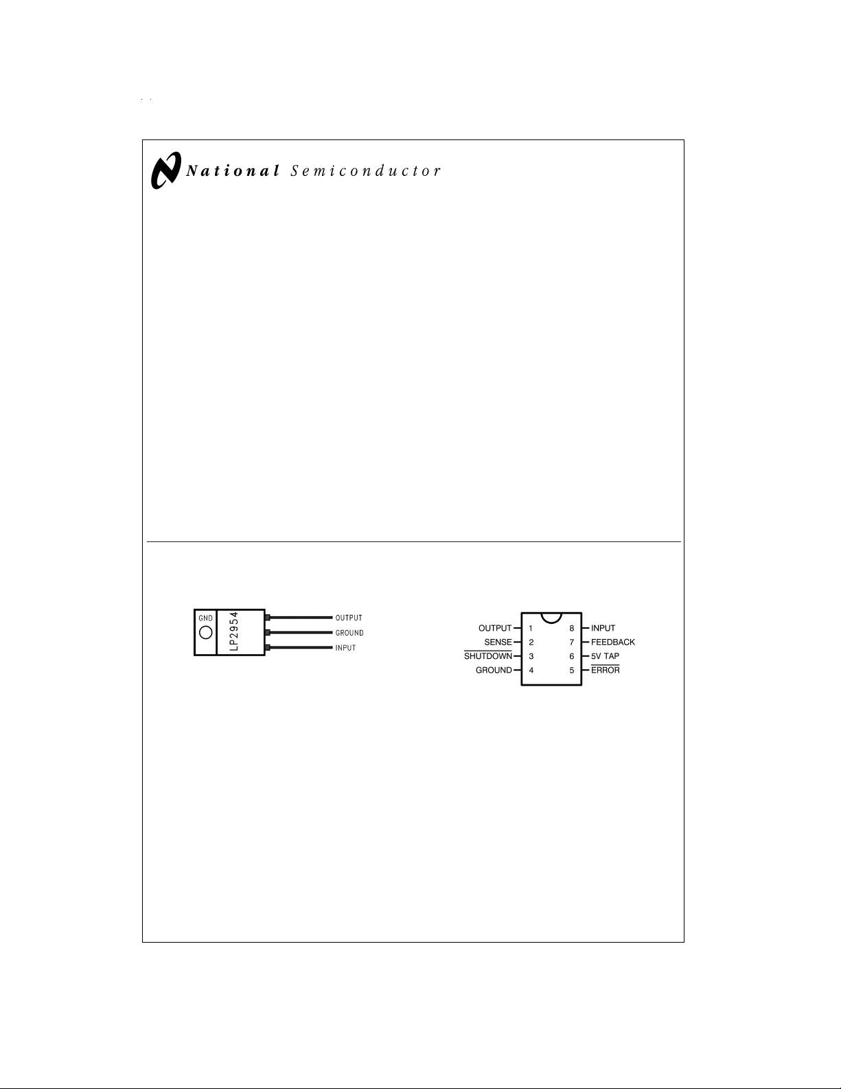
Package Outline and Ordering Information
TO-220 3–Lead Plastic Package
DS011128-2
Order Number LP2954AIT or LP2954IT
Front View
See NS Package T03B
SO-8 Small Outline Surface Mount
DS011128-33
Top View
Order Number LP2954AIM or LP2954IM
See NS Package M08A
© 1999 National Semiconductor Corporation DS011128 www.national.com
Page 2
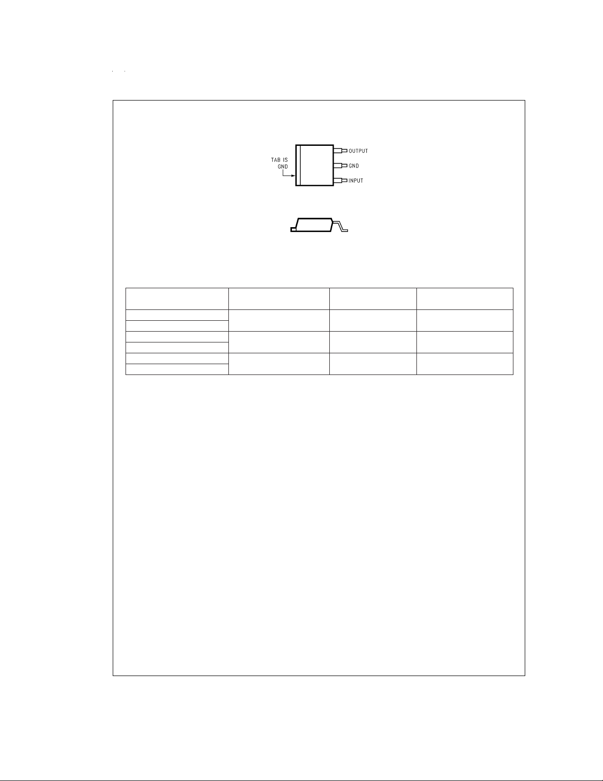
Package Outline and Ordering Information (Continued)
TO-263 3-Lead Plastic Surface-Mount Package
DS011128-9
Top View
DS011128-10
Side View
Order Number LP2954AIS or LP2954IS
See NS Package TS3B
Ordering Information
Order Number Temp. Range Package NS Package
(T
) ˚C (JEDEC) Number
LP2954AIT −40 to +125 TO-220 TO3B
LP2954IT
LP2954AIS −40 to +125 TO-263 TS3B
LP2954IS
LP2954AIM −40 to +125 SO-8 M08A
LP2954IM
J
www.national.com 2
Page 3
Absolute Maximum Ratings (Note 1)
If Military/Aerospace specified devices are required,
please contact the National Semiconductor Sales Office/
Distributors for availability and specifications.
Operating Junction Temperature
Range
LP2954AI/LP2954I −40˚C to +125˚C
Storage Temperature Range −65˚C to +150˚C
Lead Temperature
(Soldering, 5 seconds) 260˚C
Power Dissipation (Note 2) Internally Limited
Input Supply Voltage −20V to +30V
ESD Rating 2 kV
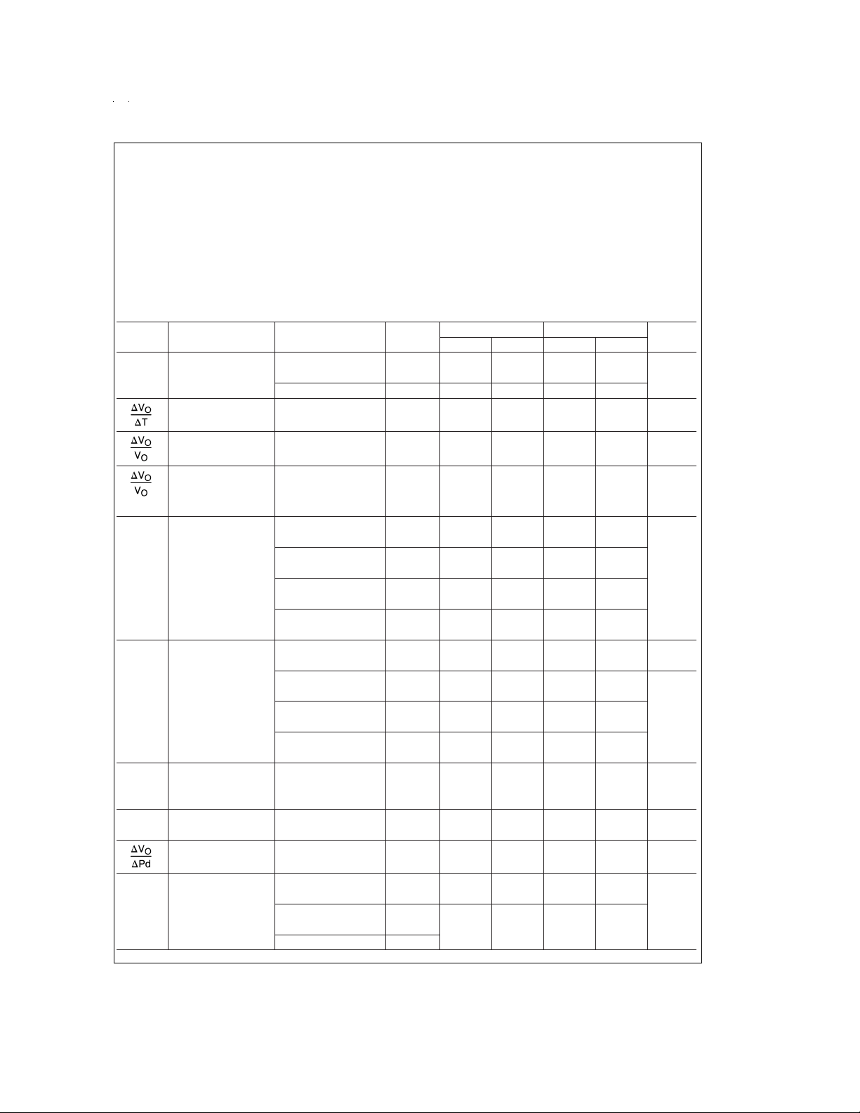
Electrical Characteristics
Limits in standard typeface are for T
are guaranteed by production testing or correlation techniques using standard Statistical Quality Control (SQC) methods. Unless otherwise noted: V
=
6V, I
IN
Symbol Parameter Conditions Typical 2954AI 2954I Units
V
O
Output Voltage 5.0 4.975 5.025 4.950 5.050 V
Output Voltage (Note 3)
Temp. Coefficient
Line Regulation V
Load Regulation I
V
IN–VO
Dropout Voltage I
(Note 5) 150 150
I
GND
Ground Pin Current I
(Note 6) 180 180
I
GND
Ground Pin V
Current at Dropout 120 210 210 µA
(Note 6)
I
LIMIT
Current Limit V
Thermal Regulation (Note 7)
=
25˚C, bold typeface applies over the −40˚C to +125˚C temperature range. Limits
J
L
=
1 mA, C
L
=
2.2 µF.
Min Max Min Max
4.940 5.060 4.900 5.100
1mA≤I
≤250 mA 5.0 4.930 5.070 4.880 5.120
L
20 100 150 ppm/˚C
=
6V to 30V 0.03 0.10 0.20
IN
0.20 0.40
=
1 to 250 mA
L
=
0.1 to 1 mA 0.04
I
L
0.16 0.20
0.20 0.30
(Note 4)
=
1 mA 60 100 100 mV
L
=
I
50 mA 240 300 300
L
420 420
=
I
100 mA 310 400 400
L
520 520
=
I
250 mA 470 600 600
L
800 800
=
1 mA 90 150 150 µA
L
=
I
50 mA 1.1 2 2 mA
L
2.5 2.5
=
I
100 mA 4.5 6 6
L
88
=
I
250 mA 21 28 28
L
33 33
=
4.5V 170 170
IN
=
0V 380 500 500 mA
OUT
530 530
0.05 0.2 0.2
%
%
%
/W
e
n
Output Noise C
=
2.2 µF 400 µV RMS
L
Voltage
(10 Hz to 100 kHz) C
=
I
100 mA
L
=
33 µF 260
L
=
33µF(Note 9) 80
C
L
www.national.com3
Page 4
Electrical Characteristics (Continued)
Limits in standard typeface are for T
are guaranteed by production testing or correlation techniques using standard Statistical Quality Control (SQC) methods. Unless otherwise noted: V
=
6V, I
IN
Symbol Parameter Conditions Typical 2954AI 2954I Units
Additional Specifications for the Adjustable Device (LP2954AIM and LP2954IM)
Reference Voltage (Note 10) 1.230 1.215
REF
/
Reference Voltage
REF
Line Regulation
REF
/∆T Reference Voltage
Temperature
∆V
V
∆V
V
REF
Coefficient
(FB) Feedback Pin Bias
I
B
I
GND
Current
Ground Pin Current
at Shutdown (Note
6)
(SINK) Output ″OFF″
I
O
Pulldown Current
Dropout Detection Comparator
I
Output ″HIGH″
OH
Leakage Current
V
V
THR
V
THR
Output ″LOW″
OL
Voltage
(MAX) Upper Threshold
Voltage
(MIN) Lower Threshold
Voltage
HYST Hysteresis (Note 13) 15 mV
Shutdown Input
V
Input Offset Voltage (Referred to V
OS
HYST Hysteresis 6 mV
I
Input Bias Current VIN(S/D)=0V to 5V 10 −30
B
Note 1: Absolute maximum ratings indicate limits beyond which damage to the component may occur. Electrical specifications do not apply when operating the device outside of its rated operating conditions.
Note 2: The maximum allowable power dissipation is a function of the maximum junction temperature, T
and the ambient temperature, T
. The maximum allowable power dissipation at any ambient temperature is calculated using:
A
=
25˚C, bold typeface applies over the −40˚C to +125˚C temperature range. Limits
J
=
L
1 mA, C
L
=
2.2 µF.
Min Max Min Max
=
V
2.5V to
IN
VO(NOM)+1V
=
2.5V to
V
IN
VO(NOM)+1V to 30V
1.205
1.255
0.03 0.1 0.2
0.2 0.4
1.245
1.205
1.190
1.255
1.270
(Note 11)
(Note 3) 20 ppm/˚C
20 40
V
SHUTDOWN
≤1.1V 105 140 140 µA
(Note 12) 30
20
=
V
30V 0.01 1
OH
=
V
(NOM)−0.5V
V
IN
O
(COMP)=400µA
I
O
150 250
(Note 13) −60 −80
−95
(Note 13) −85 −110
−160
REF
)
±
3 −7.5
−10
−50
60
30
20
2
400
−35
−25
−55
−40
7.5
10
30
50
(MAX), the junction-to-ambient thermal resistance, θ
J
−80
−95
−110
−160
−7.5
−10
−30
−50
40
60
1
2
250
400
−35
−25
−55
−40
7.5
10
30
50
nA
mA
µA
mV
mV
mV
mV
nA
V
,
J-A
Exceeding the maximum allowable power dissipation will result in excessive die temperature, and the regulator will gointothermal shutdown.The junction-to-ambient
thermal resistance of the TO-220 (without heatsink) is 60˚C/W, 73˚C/W for the TO-263, and 160˚C/W for the SO-8. If the TO-263 package is used, the thermal resistance can be reduced by increasing the P.C. board copper area thermally connected to the package: Using 0.5 square inches of copper area, θ
1 square inch of copper area, θ
If an external heatsink is used, the effective junction-to-ambient thermal resistance is the sum of the junction-to-case resistance (3˚C/W), the specified thermal resistance of the heatsink selected, and the thermal resistance of the interface between the heatsink and the LP2954. Some typical values are listed for interface materials used with TO-220:
www.national.com 4
is 37˚C/W; and with 1.6 or more square inches of copper area, θJAis 32˚C/W. The junction-to-case thermal resistance is 3˚C/W.
JA
is 50˚C/W; with
JA
.
Page 5

Electrical Characteristics (Continued)
TABLE 1. Typical Values of Case-to-Heatsink
Thermal Resistance (˚C/W) (Data from AAVID Eng.)
Silicone grease 1.0
Dry interface 1.3
Mica with grease 1.4
Note 3: Output voltage temperature coefficient is defined as the worst case voltage change divided by the total temperature range.
Note 4: Regulation is measured at constant junction temperature using low duty cycle pulse testing. Parts are tested separately for load regulation in the load
ranges 0.1 mA–1 mA and 1 mA–250 mA. Changes in output voltage due to heating effects are covered by the thermal regulation specification.
Note 5: Dropout voltage is defined as the input to output differential at which the output voltage drops 100 mV below the value measured with a 1V differential.
Note 6: Ground pin current is the regulator quiescent current. The total current drawn from the source is the sum of the load current plus the ground pin current.
Note 7: Thermal regulation is defined as the change in output voltage at a time T after a change in power dissipation is applied, excluding load or line regulation
effects. Specifications are for 200 mA load pulse at V
Note 8: When used in dual-supply systems where the regulator load is returned to a negative supply, the output voltage must be diode-clamped to ground.
Note 9: Connect a 0.1µF capacitor from the output to the feedback pin.
Note 10: V
Note 11: Two seperate tests are performed, one covering V
Note 12: V
Note 13: Comparator thresholds are expressed in terms of a voltage differential at the Feedback terminal below the nominal reference voltage measured at
=
V
(NOM)+1V. To express these thresholds in terms of output voltage change, multiply by the Error amplifier gain, which is V
V
IN
O
Note 14: Human body model, 200pF discharged through 1.5kΩ.
≤(VIN−1V), 2.3V≤VIN≤30V, 100µA≤IL≤250mA.
REF≤VOUT
≤1.1V, VOUT=VO(NOM).
SHUTDOWN
=
20V (3W pulse) for T=10 ms.
IN
=
IN
(NOM)+1V and the other test for V
2.5V to V
O
TABLE 2. Typical Values of Case-to-Heatsink
Thermal Resistance (˚C/W) (Data from Thermalloy)
Thermasil III 1.3
Thermasil II 1.5
Thermalfilm (0.002) with grease 2.2
=
IN
2.5V to V
(NOM)+1V to 30V.
O
OUT/VREF
=
(R1+R2)/R2.
Typical Performance Characteristics
Quiescent Current
Ground Pin Current
DS011128-12
DS011128-15
Quiescent Current
Ground Pin Current
DS011128-13
DS011128-16
Ground Pin Current vs Load
DS011128-14
Output Noise Voltage
DS011128-17
www.national.com5
Page 6

Typical Performance Characteristics (Continued)
Ripple Rejection
Line Transient Response
Load Transient Response
DS011128-18
DS011128-21
Ripple Rejection
Line Transient Response
Load Transient Response
DS011128-19
DS011128-22
Ripple Rejection
DS011128-20
Output Impedance
DS011128-23
Dropout Characteristics
DS011128-24
Thermal Response
DS011128-27
www.national.com 6
DS011128-25
Short-Circuit Output
Current and Maximum
Output Current
DS011128-26
DS011128-28
Page 7

Typical Performance Characteristics (Continued)
Maximum Power Dissipation
(TO-263) (See (Note 2) )
Application Hints
EXTERNAL CAPACITORS
A 2.2 µF (or greater) capacitor is required between the output pin and the ground to assure stability (refer to
Without this capacitor, the part may oscillate. Most types of
tantalum or aluminum electrolytics will work here. Film types
will work, but are more expensive. Many aluminum electrolytics contain electrolytes which freeze at −30˚C, which requires the useof solid tantalumsbelow −25˚C. Theimportant
parameters of the capacitor are an ESR of about 5Ω or less
and a resonant frequency above 500 kHz (the ESR may increase by a factor of 20 or 30 as the temperature is reduced
from 25˚C to −30˚C). The value of this capacitor may be increased without limit. At lower values of output current, less
output capacitance is required for stability.The capacitor can
be reduced to 0.68 µF for currents below 10 mA or 0.22 µF
for currents below 1 mA.
A 1 µF capacitor should be placed from the input pin to
ground if there is more than 10 inches ofwire between theinput and the AC filter capacitor or if a battery input is used.
Programming the output for voltages below 5V runs the error
amplifier at lower gains requiring more output capacitance
for stability. At 3.3V output, a minimum of 4.7 µF is required.
For the worst case condition of 1.23V output and 250 mA of
load current, a 6.8 µF (or larger) capacitor should be used.
Stray capacitance to the Feedback terminal can cause instability. This problem is most likely to appear when using high
value external resistors to set the output voltage. Adding a
100 pF capacitor between the Output and Feedback pins
and increasing the output capacitance to 6.8 µF (or greater)
will cure the problem.
MINIMUM LOAD
When setting the output voltage using an external resistive
divider, a minimum current of 1 µA is recommended through
the resistors to provide a minimum load.
It should be noted that a minimum load current is specified in
several of the electrical characteristic test conditions, so this
value must be used to obtain correlation on these tested limits. The part is parametrically tested down to 100 µA, but is
functional with no load.
Figure 1
DROPOUT VOLTAGE
The dropout voltage of the regulator is defined as the minimum input-to-output voltage differential required for the out-
).
put voltage to stay within 100 mV of the output voltage measured with a 1V differential. The dropout voltages for various
values of load current are listed under Electrical Characteristics.
If the regulator is powered from a rectified AC source with a
capacitive filter, the minimum AC line voltage and maximum
load current must be used to calculate the minimum voltage
at the input of the regulator.The minimum input voltage, in-
cluding AC ripple on the filter capacitor , must not drop
below the voltage required to keep the LP2954 in regulation.
It is also advisable to verify operating at minimum operating
ambient temperature, since the increasing ESR of the filter
capacitor makes this a worst-case test for dropout voltage
due to increased ripple amplitude.
HEATSINK REQUIREMENTS
A heatsink may be required with the LP2954 depending on
the maximum power dissipation and maximum ambient temperature of the application. Under all possible operating conditions, the junction temperature must be within the range
specified under Absolute Maximum Ratings.
To determine if a heatsink is required, the maximum power
dissipated by the regulator, P(max), must be calculated. It is
important to remember that if the regulator is powered from
a transformer connected to the AC line, the maximum
specified AC input voltage must be used (since this produces the maximum DC input voltage to the regulator).
ure 1
the circuit. The formula for calculating the power dissipated
in the regulator is also shown in
DS011128-11
Fig-
shows the voltages and currents which are present in
Figure 1
.
www.national.com7
Page 8

Application Hints (Continued)
the value of R2 in cases where the regulator must work with
no load (see MINIMUM LOAD ).I
error in V
by trimming R1. For better accuracy, choosing R2=100 kΩ
which can be eliminated at room temperature
OUT
will produce a typical 2
FB
will reduce this error to 0.17%while increasing the resistor
program current to 12 µA. Since the typical quiescent current
is 120 µA, this added current is negligible.
%
*See External Capacitors
=
−5) IL+(VIN)I
(V
P
Total
IN
G
DS011128-5
FIGURE 1. Basic 5V Regulator Circuit
The next parameter which must be calculated is the maximum allowable temperature rise, T
by using the formula:
T
(max)=TJ(max) − TA(max)
R
where: T
(max) is the maximum allowable junction
J
(max). This is calculated
R
temperature
(max) is the maximum ambient temperature
T
A
Using the calculated values for T
quired value for junction-to-ambient thermal resistance,
θ
, can now be found:
(J-A)
=
(J-A)
(max)/P(max)
T
R
θ
(max) and P(max), the re-
R
If the calculated value is 60˚ C/W or higher , the regulator
may be operated without an external heatsink. If the calculated value is below 60˚ C/W, an external heatsink is required. The required thermal resistance for this heatsink can
be calculated using the formula:
=
θ
(H-A)
− θ
(J-C)
− θ
(C-H)
θ
(J-A)
where:
is the junction-to-case thermal resistance, which is
θ
(J-C)
specified as 3˚ C/W maximum for the LP2954.
θ
is the case-to-heatsink thermal resistance, which is
(C-H)
dependent on the interfacing material (if used). For details
and typical values, refer to (Note 2) listed at the end of the
ELECTRICAL CHARACTERISTICS section.
θ
is the heatsink-to-ambient thermal resistance. It is this
(H-A)
specification (listed on the heatsink manufacturers data
sheet) which defines the effectiveness of the heatsink. The
heatsink selected must have a thermal resistance which is
equal to or lower than thevalue of θ
above listed formula.
calculated from the
(H-A)
PROGRAMMING THE OUTPUT VOLTAGE
The regulator may be pin-strapped for 5V operation using its
internal resistive divider by tying the Output and Sense pins
together and also tying the Feedback and 5V Tap pins together.
Alternatively,it may be programmed for any voltage between
the 1.23V reference and the 30V maximum rating using an
external pair of resistors (see
Figure 2
). The complete equa-
tion for the output voltage is:
where V
pin bias current (−20 nA typical). The minimum recom-
is the 1.23V reference and IFBis the Feedback
REF
mended load current of 1µA sets an upper limit of 1.2 MΩ on
*
See Application Hints
**
Drive with TTL-low to shut down
DS011128-36
FIGURE 2. Adjustable Regulator
DROPOUT DETECTION COMPARATOR
This comparator produces a logic “LOW” whenever the output falls out of regulation by more than about 5%. This figure
results from the comparator’s built-in offset of 60 mV divided
by the 1.23V reference (refer to block diagrams on page 1).
The 5%low trip level remains constantregardless of the programmed output voltage. An out-of-regulation condition can
result from low input voltage, current limiting, or thermal limiting.
Figure 3
gives a timing diagram showing the relationship between the output voltage, the ERROR output, and input voltage as the input voltage is ramped up and down to a regulator programmed for 5V output. The ERROR signal becomes
low at about 1.3V input. It goes high at about 5V input, where
the output equals 4.75V. Since the dropout voltage is load
dependent, the input voltage trip points will vary with load
current. The output voltage trip point does not vary.
The comparator has an open-collector output which requires
an external pull-up resistor. This resistor may be connected
to the regulator output or some other supply voltage. Using
the regulator output prevents an invalid “HIGH” on the comparator output which occurs if it is pulled up to an external
voltage while the regulator input voltage is reduced below
1.3V. In selecting a value for the pull-up resistor, note that
while the output can sink 400 µA, this current adds to battery
drain. Suggested values range from 100 kΩ to 1 MΩ. This
resistor is not required if the output is unused.
When V
ance, allowing the error flag voltage to rise to its pull-up voltage. Using V
nal 5V source) will keep the error flag voltage below 1.2V
≤ 1.3V, the error flag pin becomes a high imped-
IN
as the pull-up voltage (rather than an exter-
OUT
(typical) in this condition. The user may wish to divide down
the error flag voltage using equal-value resistors (10 kΩ suggested) to ensure a low-level logic signal during any fault
condition, while still allowing a valid high logic level during
normal operation.
www.national.com 8
Page 9

Application Hints (Continued)
* In shutdown mode, ERROR will go high if it has been pulled up to an
external supply. To avoid this invalid response, pull up to regulator output.
*
* Exact value depends on dropout voltage. (See Application Hints)
FIGURE 3. ERROR Output Timing
OUTPUT ISOLATION
The regulator output can be left connected to an active voltage source (such as abattery) with the regulator input power
turned off, as long as the regulator ground pin is con-
nected to ground . If the ground pin is left floating, damage
to the regulator can occur if the output is pulled up by an
external voltage source.
REDUCING OUTPUT NOISE
In reference applications it may be advantageous to reduce
theAC noise present on the output. One method is to reduce
regulator bandwidth by increasing output capacitance. This
is relatively inefficient, since large increases in capacitance
are required to get significant improvement.
DS011128-37
Typical Applications
Noise can bereduced more effectivelyby a bypass capacitor
placed across R1 (refer to
Figure 2
). The formula for select-
ing the capacitor to be used is:
This gives a value of about 0.1 µF. When this is used, the
output capacitor must be 6.8 µF (or greater) to maintain stability. The 0.1 µF capacitor reduces the high frequency gain
of the circuit to unity, lowering the output noise from 260 µV
to 80 µV using a 10 Hz to 100 kHz bandwidth.Also, noise is
no longer proportional to the output voltage, so improvements are more pronounced at high output voltages.
SHUTDOWN INPUT
A logic-level signal will shut off the regulator output when a
<
“LOW” (
1.2V) is applied to the Shutdown input.
To prevent possible mis-operation, the Shutdown input must
be actively terminated. If the input is driven from
open-collector logic, a pull-up resistor (20 kΩ to 100 kΩ recommended) should be connected from the Shutdown input
to the regulator input.
If the Shutdown input is driven from a source that actively
pulls high and low (like an op-amp), the pull-upresistor is not
required, but may be used.
If the shutdown function is not to be used, the cost of the
pull-up resistor can be saved by simply tying the Shutdown
input directly to the regulator input.
IMPORTANT: Since the Absolute Maximum Ratings state
that the Shutdown input can not go more than 0.3V below
ground, the reverse-battery protection feature which protects
the regulator input is sacrificed if the Shutdown input is tied
directly to the regulator input.
If reverse-battery protection is required in an application,
the
pull-up resistor between the Shutdown input and the regulator input must be used.
Typical Application Circuit
5V Regulator
DS011128-1
DS011128-6
www.national.com9
Page 10

Typical Applications (Continued)
5V Current Limiter
*Output voltage equals +VINminus dropout voltage, which varies with output current. Current limits at 380 mA (typical).
DS011128-7
Schematic Diagram
www.national.com 10
DS011128-8
Page 11

Physical Dimensions inches (millimeters) unless otherwise noted
TO-220 3-Lead Plastic Package
Order Number LP2954AIT or LP2954IT
NS Package T03B
www.national.com11
Page 12

Physical Dimensions inches (millimeters) unless otherwise noted (Continued)
TO-263 3-Lead Plastic Surface Mount Package
Order Number LP2954AIS or LP2954IS
www.national.com 12
NS Package TS3B
Page 13

Physical Dimensions inches (millimeters) unless otherwise noted (Continued)
SO-8 Surface Mount Package
Order Number LP2954AIM or LP2954IM
NS Package Number M08A
LP2954/LP2954A 5V and Adjustable Micropower Low-Dropout Voltage Regulators
LIFE SUPPORT POLICY
NATIONAL’S PRODUCTS ARE NOT AUTHORIZED FOR USE AS CRITICAL COMPONENTS IN LIFE SUPPORT
DEVICES OR SYSTEMS WITHOUT THE EXPRESS WRITTEN APPROVAL OF THE PRESIDENT AND GENERAL
COUNSEL OF NATIONAL SEMICONDUCTOR CORPORATION. As used herein:
1. Life support devices or systems are devices or
systems which, (a) are intended for surgical implant
into the body, or (b) support or sustain life, and
whose failure to perform when properly used in
accordance with instructions for use provided in the
2. A critical component is any component of a life
support device or system whose failure to perform
can be reasonably expected to cause the failure of
the life support device or system, or to affect its
safety or effectiveness.
labeling, can be reasonably expected to result in a
significant injury to the user.
National Semiconductor
Corporation
Americas
Tel: 1-800-272-9959
Fax: 1-800-737-7018
Email: support@nsc.com
www.national.com
National does not assume any responsibility for use of any circuitry described, no circuit patent licenses are implied and National reserves the right at any time without notice to change said circuitry and specifications.
National Semiconductor
Europe
Fax: +49 (0) 1 80-530 85 86
Email: europe.support@nsc.com
Deutsch Tel: +49 (0) 1 80-530 85 85
English Tel: +49 (0) 1 80-532 78 32
Français Tel: +49 (0) 1 80-532 93 58
Italiano Tel: +49 (0) 1 80-534 16 80
National Semiconductor
Asia Pacific Customer
Response Group
Tel: 65-2544466
Fax: 65-2504466
Email: sea.support@nsc.com
National Semiconductor
Japan Ltd.
Tel: 81-3-5639-7560
Fax: 81-3-5639-7507
 Loading...