

Datasheet LP2951AM-3, LP2951AM, LP2951BM-5, LP2951BM-3.3, LP2951BM-3 Datasheet (Bay Linear)
...Page 1
Bay Linear, Inc
2478 Armstrong Street, Livermore, CA 94550 Tel: (925) 989-7144, Fax: (925) 940-9556 www.baylinear.com
100mA Low Dropout Voltage Regulator
LP2950/LP2951
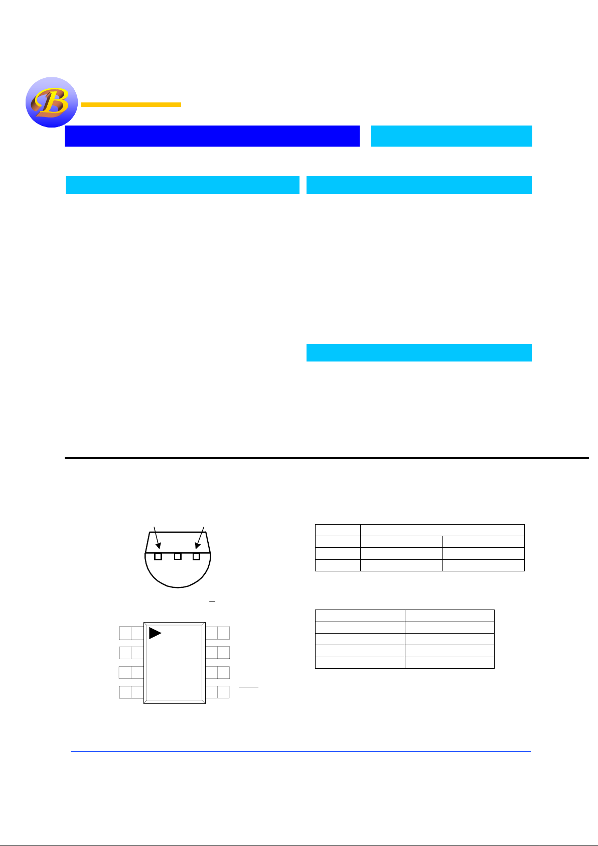
Pin Connection
TO-92 (Z)
Ordering Information
8SOIC (M)
Package Tolerance
0.5% 1%
TO-92
LP2950AZ-XX LP2950-BZ-XX
8SOIC
LP2951AM-XX LP2951BM-XX
“XX” Voltage Selection Guide
Vout XX Code
5.0V
5
3.3V
3.3
3.0V
3
Adjustable
Left Blank
Description
The Bay Linear LP2950 and LP2951 are low power voltage
regulators. They are excellent choice for use in Battery
Powered applications such notebooks computers. The LP2950
and LP2951 feature low quiescent current ( 75µA Typ.) and
low dropout of 40mV at light loads 380mV (typ.) at 100mA.
With a tight initial tolerance of 0.5% typ., extremely good load
and line regulation of 0.05% typ. And very low output
temperature coef ficien t makin g th e LP 2950 an d LP2 95 1 u seful
as a low power reference.
The Bay Linear LP2950 is available in fixed voltages of 3.0V,
3.3V, and 5.0V in a TO-9 2 package.
The Bay Linear LP2951 co mes in an 8SOIC package and h as
an adjustable output voltage from 1.24V to 29V programmed
with a pair of external resistor. It also features pin-strap
capability providing the fixed voltage of 3.0, 3.3V or 5V for
convenience. The LP29 51 has an error flag ou tpu t feature used
as power-on reset for warning of low output voltage due to
falling battery voltages. Also, the logic compatible shutdown
input enables the regulator to be switched ON and OFF.
Features
•
Guaranteed 100mA Output
•
5.0V, 3.3V and 3.0V Versions
•
Very Low Quiescent Current
•
Low Dropout Voltage
•
Extremely Tight Load and Line
Regulation
•
Very Low Temperature Coefficient
•
Needs only 1µµµµF for Stability
•
Error Flag warns of output dropout
•
Logic-Controlled Electronic Shutdow n
•
Output programmable from 1.24V to 29V
Applications
• Battery Powered Systems
• Portable instrumentation
• Notebooks Computers
• Potable Consumer Equipment
• Automotive electronics
• SMPS Post-Regulator
Bay Linear
Bay LinearBay Linear
Bay Linear
Linear Excellenc e
1
2
4
3
5
6
7
8
Output
Input
Shutdown
Sense
-XX V tap
Feedback
Ground
Error
Vout
Vin
Grd
Page 2
Bay Linear, Inc
2478 Armstrong Street, Livermore, CA 94550 Tel: (925) 989-7144, Fax: (925) 940-9556 www.baylinear.com
LP2950/LP2951
Absolute Maximum Rating
Parameter
Power Dissipation Internally Limited
Lead Temperature ( Soldering 5 seconds )
260 °C
Storage Temperature Range
-65 °C to +150 °C
Operating Junction Temperature
-55 °C to +150 °C
Input Supply Voltage -0.3V to +30V
Feedback Input Voltage -1.5V to +30V
Shutdown Input Voltage -0.3V to +30V
Error Comparator Output -0.3V to +30V
Electrical Characteristics
(VS = 15V, TA = 25°C , unless otherwise specified)
Parameter Conditions MIN TYP MAX UNIT
Output Voltage
-25 °C ≤ T
j
≤
85 °C
Full Operating Temperature
0.985 [ V
o
]
0.98 [ V
o
]
V
o
1.015 [ Vo ]
1.02 [ V
o
]
V
Output Voltage
100µA ≤ I
L
≤
100mA, T
j
≤ T
jmax
0.976 [Vo ] Vo 1.024 [ Vo ]
V
Output Voltage Temperature
Coefficient
(Note 1) 50 150
ppm / ° C
Line Regulation (Note 3)
V
O
+ 1V ≤ VIN ≤ 30V (Note 4)
0.04 0.4 %
Load Regulation (Note 5)
100µA ≤ I
L
≤
100mA
0.1 0.3 %
Dropout Voltage
I
L
= 100µA
IL = 100mA
50
380
80
450
mV
Ground Current
I
L
= 100µA
IL = 100mA
75 8 120
12
µ
A
mA
Dropout Ground Current
V
IN
= VO - 0.5V, IL = 100µA
110 170
µ
A
Current Limit V
OUT
= 0 160 200 mA
Thermal Regulation 0.05 0.2 % / W
Output Noise,
10Hz to 100KHz
C
L
= 1µF
C
L
= 200µF
C
L
= 3.3µF
(Bypass = 0.01 µF pins 7 to 1 for
LP2951-XX)
430
160
100
µ
Vrms
8 pin Versions only (LP2951)
Reference Voltage
Over temperature
1.21
1.185
1.235 1.26
1.285
V
Feedback Pin Bias Current 20 40
η
A
Reference Voltage Temperature
Coefficient
(Note 7) 50
ppm/°C
Feedback Pin Bias Current
Temperature Coefficient
0.1 100
ηA/°
C
Error Comparator
Output Leakage Current VOH = 30V 0.01 1.0
µ
A
Output Low Voltage
V
IN
4.5V, IOL = 400µA
150 250 mV
Upper Threshold Voltage (Note 8) 40 60 mV
Lower Threshold Voltage (Note 8) 75 95 mV
Hysteresis (Note 8) 15 mV
Page 3
Bay Linear, Inc
2478 Armstrong Street, Livermore, CA 94550 Tel: (925) 989-7144, Fax: (925) 940-9556 www.baylinear.com
LP2950/LP2951
Parameter Conditions MIN TYP MAX UNIT
Shutdown Input
Input Logic Vol tage Low (Regulator ON)
High (Regulator OFF)
2
1.3 0.7 V
Shutdown Pin Input Current VS = 5V
V
S
=30V
30
450
50
600
µ
A
Regulator Output Current
in Shutdown
(Note 9)
V
OUT
= 5.0V
3.3V ≤ V
OUT
≤
5.0V
2.0V ≤ V
OUT
≤
3.3V
3
10
20
30
µ
A
Note 1:
Output or reference voltage temperature coefficient s defined as the worst case voltage change di vided by the total temperature range.
Note 2:
Unless otherwise sp ecified all limits guaranteed for T
J
= 25°C, VIN = VO +1V, IL = 100µA and CL = 1µF. Additional conditions for the 8-
pin versions are feedback tied to –XX Voltage tap and output tied to output Sense pin ( V
OUT
= XX V) and V
SHUTDOWN
≤ 0.8V
Note 3:
Regulation is meas ured at constant junction temperat ure , using pulse testing with a low dut y cycle. Changes in output voltage due to
heating effects are covered under sp ecification for therm al regulation.
Note 4:
Line regulation for LP2951-XX is tested at 150°C for I
L
= 1mA. For IL = 100µA and TJ = 125°C, line regulation is guaranteed by design
to 0.2%. See typical performance characteristics for line regulation versus temperature and load current.
Note 5:
Dropout voltage is defi ned as the input to output differential at which the output voltage drops 100mV below its nominal value measured
at 1V differenti al. At very low values of programmed output voltage, the minimum input supply voltag e of 2V (2.3V over tempera ture) must be
taken into account.
Note 6:
V
REF
≤ V
OUT
≤ (V
IN
–1V), 2.3V ≤ VIN ≤ 30V, 100µA ≤ IL ≤100mA, T
J
≤ T
JMAX
Note 7:
Output or reference voltage temperature coefficient is defined as the worst case voltage change divided by the total temperature range
Note 8:
Comparator thresholds are expressed in terms of a voltage differential at the feedback terminal below the nominal reference voltage
measured at V
O
+ 1V input. To express these thresholds in terms of output voltage change, multiply by the error amplifier gain = V
OUT
/ V
REF
=
(R1 + R2)/R2. For example, at a programmed output voltage of 5V, the error output is guaranteed to go low when the output drops by 95mV X
5V / 1.235V = 384mV. Thresholds remain constant as a percent of V
OUT
as V
OUT
is varied, with the dropout warning oc curring at typically 5%
below nominal, 7.5% guaranteed.
Note 9:
V
SHUTDOWN
≥ 2V, VIN ≤ 30V, V
OUT
= 0, Feed-back pin tied to –XX Voltage Tap.
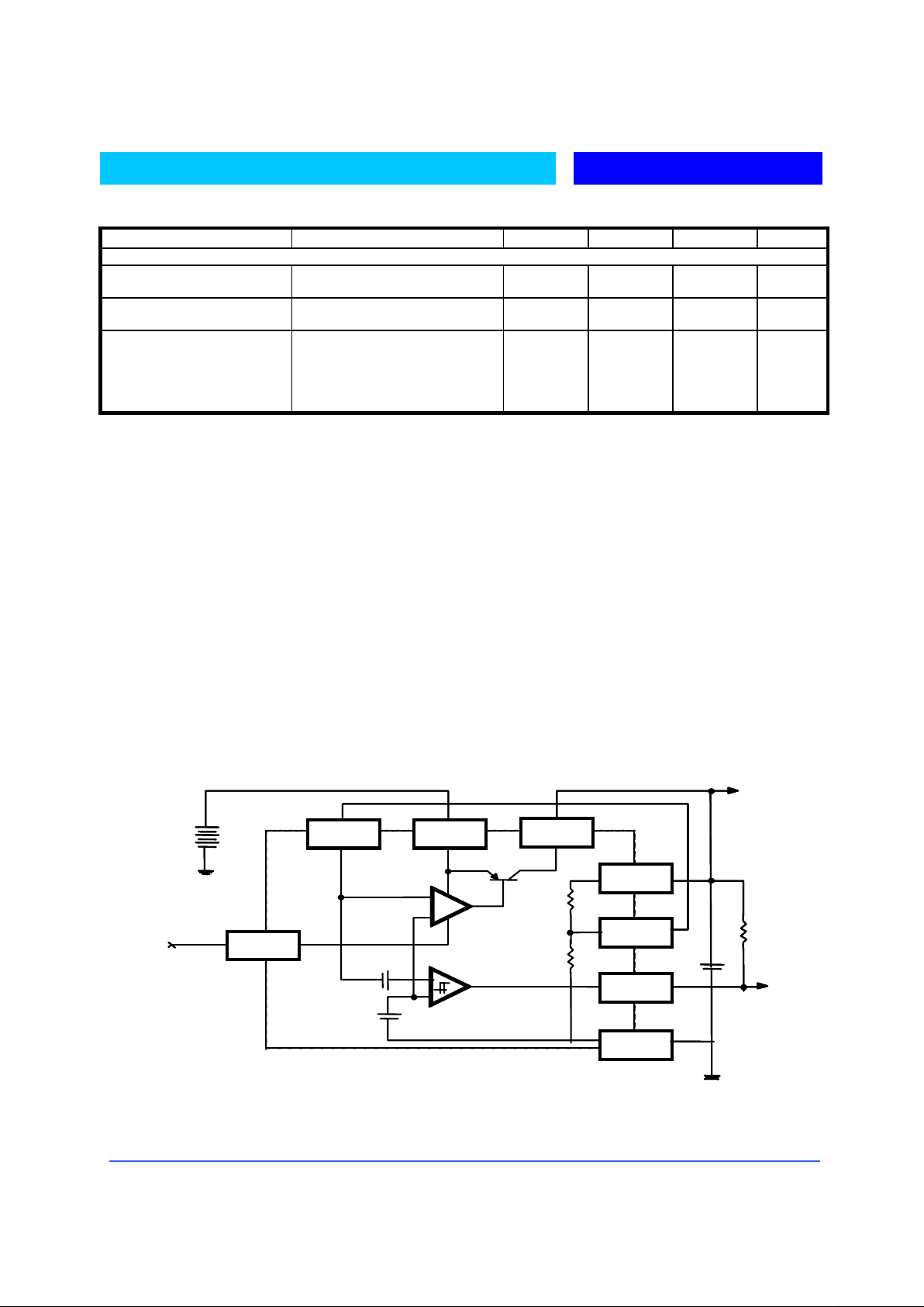
Block Diagram
FEEDBACK
INPUT
OUTPUT
UNREGULATED DC
SHUTDOWN
GROUND
ERROR
______
5V TAP
SENSE
5V @ 150mA
MAX
TO CMOS OR
TTL
REFERENCE
ERROR DETECTION
COMPARATOR
ERROR
AMPLIFIER
1.23V
FROM
CMOS OR
TTL
+
+
+
+
+
+
60 mV
3
7
8
1
2
6
5
4
Ω
..
60k
330k
180k
Ω
..
Ω
..
µ
..1F
_
_
LP2950 and LP2951 Block Diagram
FEEDBACK
INPUT
OUTPUT
UNREGULATED DCUNREGULATED DC
SHUTDOWN
GROUND
ERROR
______
5V TAP
SENSE
5V @ 150mA
MAX
5V @ 150mA
MAX
TO CMOS OR
TTL
TO CMOS OR
TTL
REFERENCE
ERROR DETECTION
COMPARATOR
ERROR DETECTION
COMPARATOR
ERROR
AMPLIFIER
ERROR
AMPLIFIER
1.23V
FROM
CMOS OR
TTL
FROM
CMOS OR
TTL
+
+
+
+
+
+
60 mV
3
7
8
1
2
6
5
4
Ω..Ω
..
60k
330k
180k
Ω..Ω
..
Ω..Ω
..
µ..µ
..1F
_
_
LP2950 and LP2951 Block Diagram
Page 4
Bay Linear, Inc
2478 Armstrong Street, Livermore, CA 94550 Tel: (925) 989-7144, Fax: (925) 940-9556 www.baylinear.com
LP2950/LP2951
APPLICATION HINTS
EXTERNAL CAPACITORS
The stability of the LP2950/LP2951 requires a 1.0µF or greater
capacitor between output and ground. Oscillation could occur
without this capacitor. Most types of tantalum or aluminum
electrolytic works fine here. For operations below -25°C solid
tantalum is recommended since many aluminum types have
electrolytes that freez e at about -30°C. The ESR of about 5Ω or
less and resonant frequency above 500kHz are the most important
parameters in the value of th e capacitor. The capaci tor value can
be increased without limit.
At lower values of output current, less output capacitance is
required for stability. For the currents below 10mA the value of
the capacitor can be reduced to 0.5µF and 0.15µF for 1mA. More
output capacitance is needed for the 8-pin version at voltages
below 5V since it runs the error amplifier at lower gain. At worst
case 5µF or greater must be used for the condition of 150mA load
at 1.23V output.
The LP2950, unlike other low dropout regulators will remain
stable in regulation with no load in addition to the internal voltage
divider. This feature is especially important in applications like
CMOS RAM keep-alive. When setting the output volt age of the
LP2951 version with external resistors, a minimum load of 1uA is
recommended.
If there is mor e than 10 inches of wire between the input and the
AC filter cap acitor or if a battery is used as th e input then a 1µA
tantalum or aluminum electrolytic capacitor should be placed from
the input to the ground.
Instability can occur if there is stray capacitance to the LP2951
feedback terminal (pin 7). This could cause more problems when
using a higher va lue of extern al resis tors to set the ou tput volt age.
This problem can be fixed by adding a 100pF capacitor between
output and feedb ack and in creas ing the outpu t capac itor to at least
3.3µF.
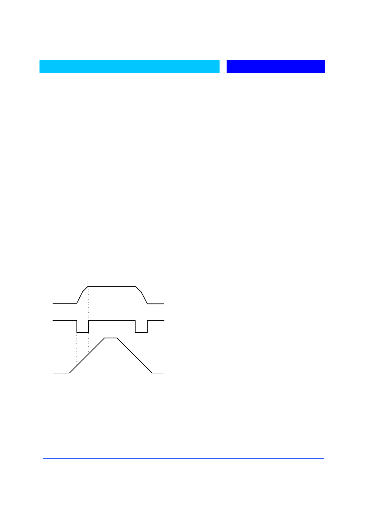
ERROR DETECTION COMPARATOR
OUTPUT
The Comparator produces a logic low output whenever the
LP2951 output fa lls out of regulation by more than around 5%.
This is around 60mV offset divi ded by t he 1.23 5 referen ce volt age.
This trip level remains 5% below normal regardless of the
programmed outp ut voltage of the regulator. Figure 1 shows the
timing diagram depicting the ERROR signal and the regulator.
output voltage as the LP2951 input is ramped up and down. The
ERROR signal becomes low at around 1.3V input, and goes high
around 5V input (input voltage at which V
OUT
= 4.75 ). Since the
LP2951’s drop out voltage is loa d dependent, the input volta ge trip
point (around 5V) will vary with the load current. The output
voltage trip poin t (approx. 4.75V) does not vary with load
The error comparator has an open-collector output which requires
an external pull-up resistor. Depending on the system requirements
the resistor ma y be retu rned to 5 V output or oth er supp ly volta ge in
determining the value of this resistor, note that the output is rated to
sink 400µA, this value adds to battery drain in a low battery
condition. Suggested values range from 100K to 1MΩ. If the
output is unused this resistor is not required.
PROGRAMMING THE OUTPUT VOLTAGE OF
LP2951
The LP2951 may be pin-strapped for 5V using its internal voltage
divider by tying Pin 1 (output) to Pin 2 (sense) and Pin 7 (feedback)
to Pin 6 (5V Tap). Also it may be programmed for any output
voltage between i ts 1.235 V referenc e and it s 30V maximu m ratin g .
As seen in Figure 2, an external pair of resistors is required.
Refer to the below equation for the programming of the output
voltage.
V
OUT
= V
REF
× ( 1 + R1/R2 )+ IFBR
1
The V
REF
is 1.235 and IFB is the feedback bias current, nominally
-20 nA. The minimum recommended load current of 1µA forces an
upper limit of 1.2 MΩ on value of R
2
. If no load presented the IFB
produces an error of typi call y 2% in V
OUT
which may be eliminated
at room temperature by trimming R
1
. To improve the accuracy
choose the valu e of R
2
= 100k this reduces th e error by 0.17% and
increases the resistor program current by 12µA. Since the LP2951
typically draws 60µA at no load with Pin 2 open-circuited this is a
small price to pay.
REDUCING OUTPUT NOISE
It may be an advantage to reduce the AC noise present at the output.
One way is to reduce the regulator bandwidth by increasing the size
of the output capacitor. This is the only way that noise can be
reduced on the LP2950 but is relatively inefficient, as increasing the
capacitor from 1µF to 220 µF only decreases the noise f rom 4 30µV
to 160µV
RMS
. for a 100kHz bandwidth at 5V output.
Noise could also be reduced fourfold by a bypass capacitor across
R
1
, since it reduces the high frequency gain from 4 to unity. Pick
C
BYPASS
≅ 1 / 2πR
1
× 200 Hz
or choose 0.01 µF. When doing this, the output capacitor must be
increased to 3.3µF to maintain st ability. Th ese chan ges reduc e the
output noise from 4 30µV to 100µV
RMS
. for a 100kHz bandwidth at
5V output. With the bypass capacitor added, noise no longer scales
with output voltage so that improvements are more dramatic at
higher output volt ages.
+
+
+
+
4.75V
OUTPUT
VOLTAGE
ERROR*
_______
INPUT
VOLTAGE 1.3V
5.0V
Figure 1. ERROR Output Timing
_______
* See Application Info.
Page 5

Bay Linear, Inc
2478 Armstrong Street, Livermore, CA 94550 Tel: (925) 989-7144, Fax: (925) 940-9556 www.baylinear.com
LP2950/LP2951
TYPICAL PERFORMANCE CHARACTERISTICS
INPUT CURRENT (mA)
160
150
140
130
70
50
0
INPUT VOLTAGE (VOLTS)
GROUND PIN CURRENT (mA)
10
1
0.1
0.01
0.1 1 10 150
LOAD CURRENT (mA)
120
110
100
90
80
60
40
30
20
10
0
12345678910
INPUT CURRENT
QUIESCENT CURRENT
240
220
200
180
-75
-50
-25 0 25 50 75 100 125150
TEMPERATURE (ºC)
QUIESCENT CURRENT
QUIESCENT CURRENT (µA)
170
150
130
110
-75
-50
-25 0 25 50 75 100 125150
TEMPERATURE (ºC)
SHORT CIRCUIT CURRENT
SHORT CIRCUIT CURRENT (mA)
160
140
120
110
VIN=6V
I
L
=100mA
RL=50
Ω
600
400
300
50
-75
-50
-25 0 25 50 75 100 125150
TEMPERATURE (ºC)
DROP-OUT VOLTAGE
DROP-OUT VOLTAGE (mV)
500
100
0
OUTPUT VOLTAGE (V)
5.06
5.04
5.0
TEMPERATURE (ºC)
OUTPUT VOLTAGE (VOLTS)
0
0
INPUT VOLTAGE (VOLTS)
5.02
4.98
4.96
4.94
OUTPUT VOLTAGE VS. TEMP OF 3
REPRESENTATIVE UNITS
DROPOUT CHARACTERISTICS
16
12
8
4
-75
-50
-25 0 25 50 75 100 125150
TEMPERATURE (ºC)
GROUND CURRENT
GROUND CURRENT (mA)
123456
1
2
3
4
5
6
-75
-50
-25 0 25 50 75 100 125 150
0.2%
IL = 100mA
IL = 100µA
RL=50k
Ω
RL=50k
Ω
VIN = 6V
I
L
= 100mA
~
~
INPUT CURRENT (µA)
75
0
0
10 150
INPUT VOLTAGE (VOLTS)
INPUT CURRENT
GROUND CURRENT (µA)
320
280
0
INPUT VOLTAGE (VOLTS)
240
80
40
0
12345678
GROUND CURRENT
16
14
12
0
1
2345678
INPUT VOLTAGE
GROUND CURRENT
GROUND CURRENT
RL = 50k
Ω
25
50
100
125
150
175
200
225
250
123
120
160
200
10
8
6
4
2
0
IL= 1mA
IL= 0
IL=100mA
TJ = 25ºC
DROP-OUT VOLTAGE
OUTPUT CURRENT
DROP-OUT VOLTAGE (mV)
100mA
10mA
1mA100µA
500
400
300
200
100
0
RL =
8
Page 6

Bay Linear, Inc
2478 Armstrong Street, Livermore, CA 94550 Tel: (925) 989-7144, Fax: (925) 940-9556 www.baylinear.com
LP2950/LP2951
TYPICAL PERFORMANCE CHARACTERISTICS (continued)
10
0.5
0.1
0.02
10 100 1K 10K 100K 1M
FREQUENCY (Hz)
OUTPUT IMPEDANCE
OUTPUT IMPEDANCE (OHMS)
5
0.2
0.05
0.01
90
70
60
40
10
1102103104105106
FREQUENCY (Hz)
RIPPLE REJECTION
RIPPLE REJECTION (dB)
80
50
20
RIPPLE REJECTION
FREQUENCY (Hz)
RIPPLE REJECTION (dB)
10
6
10
3
10
2101
90
80
70
60
50
20
1
2
30
IL = 100µA
IL = 0
CL = 1µF
VIN = 6V
V
OUT
= 5V
40
30
10
4105
IL = 10mA
IL = 10mA
CL= 1µF
VIN = 6V
V
OUT
= 5V
IO = 100mA
IO = 100µA
IO = 1mA
V
OUT
= 5V
CL = 1µF
COMPARATOR OUTPUT (V)
8
6
0
INPUT VOLTAGE (V)
4
2
0
-2
12345
ERROR COMPARATOR OUTPUT
SINK CURRENT (mA)
2.5
1.5
OUTPUT LOW VOLTAGE (V)
2.0
1.0
0.5
0.0
COMPARATOR SINK CURRENT
TIME(µs)
0.0
0.1
0.2 0.3 0.4 0.5 0.6 0.7 0.8 0.9
V
OUT
= 5V
PULLUP RESISTOR TO
SEPARATE 5V SUPPLY
HYSTERESIS
100
0 200
400
600 800
LINE TRANSIENT RESPONSE
INPUT OUTPUT VOLTAGE
VOLTAGE CHANGE
4V
6V
8V
-50
0
50
~
~
mV
mV
mV
CL = 1µF
IL = 1mA
V
OUT
= 5V
TA = -55ºC
TA = 25ºC
TA = 125ºC
LP2951
7
6
4
-1000100 200 300 400 500 600 700
TIME
ENABLE TRANSIENT
SHUTDOWN OUTPUT
PINOUT VOLTAGE (V) VOLTAGE (V)
3
2
1
0
2
-2
250
100
-50
100
012345
TIME (ms)
LOAD TRANSIENT RESPONSE
LOAD OUTPUT VOLTAGE
CURRENT CHANGE (mV)
µA
~
~
mA
-100
0
50
150
200
CL = 1µF
V
OUT
= 5V
80
20
-40
100
048121620
TIME (ms)
LOAD TRANSIENT RESPONSE
LOAD OUTPUT VOLTAGE
CURRENT CHANGE (mV)
µA
100
-60
-20
0
40
60
µA
CL = 1µF
V
OUT
= 5V
0
5
CL = 10µF V
OUT
= 5V
VIN = 8V
IL = 10mA
100
~
~
MINIMUM OPERATING VOLTAGE (V)
10
1
0.1
0.01
-75 0 75 150
TEMPERATURE
MINIMUM OPERATING VOLTAGE
BIAS CURRENT (nA)
-30
-75
TEMPEATURE (ºC)
FEEDBACK BIAS CURRENT
FEEDBACK CURRENT (µA)
-150
-250
-2.0
-0.5 1.0
FEEDBACK VOLTAGE (V)
FEEDBACK PIN CURRENT
-50 0 50 75 100 150
-20
-10
0
10
20
-200
-100
-50
0
50
-1.5 -1.0
-50 -25 25 50 100 125 -25 25 125 0 0.5
TA = 25ºC
TA = 55ºC
TA =1 25ºC
LP2951
LP2951
LP2951
PIN 7 DRIVEN BY EXTERNAL
SOURCE (REGULATOR RUN
OPEN LOOP)
Page 7

Bay Linear, Inc
2478 Armstrong Street, Livermore, CA 94550 Tel: (925) 989-7144, Fax: (925) 940-9556 www.baylinear.com
LP2950/LP2951
TYPICAL PERFORMANCE CHARACTERISTICS (continued)
VOLTAGE NOISE
SPECTRAL DENSITY (µV/Hz)
3.5
2.5
2.0
0.0
10
2
10
3
10
4
10
5
FREQUENCY (Hz)
OUTPUT NOISE
IL = 100mA
CL = 1µF
CL = 220µF
CL = 3.3µF
3.0
1.5
1.0
0.5
OUTPUT CURRENT (mA)
120
100
60
40
0
INPUT VOLTAGE (V)
80
20
0
510 15202530
LP2950 MAXIUM RATED OUTPUT
CURRENT
T
JMAX
= 125º C
V
OUT
= 5V
TA = 25ºC
TA = 50ºC
TA = 85ºC
8-PIN
MOLDED
DIP SOLDERED
TO PC BOARD
SHUTDOWN THRESHOLD VOLTAGE (V)
1.8
1.6
1.0
-75
TEMPERATURE (ºC)
1.4
1.2
0.8
0.6
-50 -25 0 25 50 75 100 125 150
SHUTDOWN THRESHOLD VOLTAGE
OUTPUT CURRENT (mA)
120
80
0
010 20 30
INPUT VOLTAGE (V)
LP2950 MAXIUM RATED OUTPUT
25155
TA = 85 ºC
TA=25 ºC
T
JMAX
= 125 ºC
0.25" LEADS SOLDERED
TO-92 PACKAGE
TO PC BOARD
100
60
40
20
RIPPLE REJECTION (dB)
80
60
40
10
10
1
10310
4
10
6
FREQUENCY (Hz)
RIPPLE REJECTION
IL = 50µA
IL = 100mA
CL = 1µF
VIN = 6V
V
OUT
= 5V
70
50
30
20
10
2
10
5
OUTPUT VOLTAGE CHANGE (mV)
30
25
20
10
5
INPUT VOLTAGE (V)
15
10
5
0
5
0
-5
-10
10 15 20 25 30
LINE REGULATION
~
~
IL = 100µA
IL = 1mA
TJ = 150 ºC
TJ = 125 ºC IL = 100µA
PIN 2 TO PIN 4 RESISTANCE (k
Ω)
Ω)Ω)
Ω)
400
200
100
0
-75 0 75 150
TEMPERATURE (ºC)
LP2951 DIVIDER RESISTANCE
-50 -25 25 50 100 125
300
POWER OUTPUT VOLTAGE
DISSIPATION (W) CHANGE (mV)
4
2
1
0
TIME (µs)
0
-2
0
-1
10 20 30 40 50
THERMAL RESPONSE
5
1.25W
~
~
Page 8

Bay Linear, Inc
2478 Armstrong Street, Livermore, CA 94550 Tel: (925) 989-7144, Fax: (925) 940-9556 www.baylinear.com
LP2950/LP2951
TYPICAL APPLICATIONS
(continued)
100K
SENSE
SD
V
OUT
GND
+V
IN
3
8
1
1uF
+
4
Ω
..
Ω
..
400K
120K
1.5K
Ω
..
Ω
..
6V
SEALED
LEADACID
BATTERY
SOURCE
FB
FOR 5.5 V
+
1N457
2
Ω
..
20K
NI-CAD
BACKUP
BATTERY
MEMORY V+
MAIN V-
LM385
Low Battery Disconnect
BAY
LP2951
100K
SENSE
SD
V
OUTVOUT
GND
+V
IN+VIN
3
8
1
1uF+1uF
+
4
Ω..Ω
..
Ω..Ω
..
400K
120K
1.5K
Ω..Ω
..
Ω..Ω
..
6V
SEALED
LEADACID
BATTERY
SOURCE
6V
SEALED
LEADACID
BATTERY
SOURCE
FB
FOR 5.5 V
+
1N457
2
Ω..Ω
..
20K
NI-CAD
BACKUP
BATTERY
NI-CAD
BACKUP
BATTERY
MEMORY V+
MAIN V-
LM385
Low Battery Disconnect
BAY
LP2951
GND
4
3
5
8
2
1
7
6
SD
TAP
FB
+V
IN
SENSE
V
OUT
ERROR
______
RESET
100k
100k
100k
1k
100k
10k
20k
1k
39k
39k
C3
C1
C2
C4
1%
1%
1%
1%
6V
LEADACID
BATTERY
R
3
<6.2V**
<5.8V**
<6.0V**
-
+
+
+
+
-
-
-
Ω
..
Ω
..
Ω
..
Ω
..
Ω
..
Ω
..
Ω
..
Ω
..
Ω
..
Ω
..
+V
OUT
= 5V
1uF
+
RegulatorwithState-of-Charge indicator
* OPTIONAL LATCH OFF WHEN DROPOUT OCCURS. ADJUST R3 FOR C2 SWI TCHING WHEN
V
IN
IS 6.0V
** OUTPUTS GO LOW WHEN V
IN
DROPS BELOW DESGNATED THRESHHOLDS
BAY
LP2951
GND
4
3
5
8
2
1
7
6
SD
TAP
FB
+V
IN+VIN
SENSE
V
OUTVOUT
ERROR
______
RESET
100k
100k
100k
1k
100k
10k
20k
1k
39k
39k
C3
C1
C2
C4
1%
1%
1%
1%
6V
LEADACID
BATTERY
6V
LEADACID
BATTERY
R
3R3
<6.2V**<6.2V**
<5.8V**<5.8V**
<6.0V**<6.0V**
-
+
+
+
+
-
-
-
Ω..Ω
..
Ω..Ω
..
Ω..Ω
..
Ω..Ω
..
Ω..Ω
..
Ω..Ω
..
Ω..Ω
..
Ω..Ω
..
Ω..Ω
..
Ω..Ω
..
+V
OUT
= 5V+V
OUT
= 5V
1uF
+
RegulatorwithState-of-Charge indicator
* OPTIONAL LATCH OFF WHEN DROPOUT OCCURS. ADJUST R3 FOR C2 SWI TCHING WHEN
V
IN
IS 6.0V
** OUTPUTS GO LOW WHEN V
IN
DROPS BELOW DESGNATED THRESHHOLDS
* OPTIONAL LATCH OFF WHEN DROPOUT OCCURS. ADJUST R3 FOR C2 SWI TCHING WHEN
V
IN
IS 6.0V
** OUTPUTS GO LOW WHEN V
IN
DROPS BELOW DESGNATED THRESHHOLDS
BAY
LP2951
Page 9

Bay Linear, Inc
2478 Armstrong Street, Livermore, CA 94550 Tel: (925) 989-7144, Fax: (925) 940-9556 www.baylinear.com
LP2950/LP2951
TYPICAL APPLICATIONS
(continued)
EXTERNAL CIRCUIT
PROTECTED FROM
OVER TEMPERATURE
(V+ GOES OFF WHEN
TEMP > 125)
OR
RELAY
8.2K
TEMP
SENSOR
GND
V
OUT
FB
SD
+V
IN
+V
IN
10K
5 DEGREE SHUTDOWN FLAG
ERROR
_______35
8
4
7
1
AUX SHUTDOW
INPUT
OFF
ON
Ω
..
LM35
+
-
System Over Temperature Protection Circuit
BAY
LP2951
Ω
..
EXTERNAL CIRCUIT
PROTECTED FROM
OVER TEMPERATURE
(V+ GOES OFF WHEN
TEMP > 125)
EXTERNAL CIRCUIT
PROTECTED FROM
OVER TEMPERATURE
(V+ GOES OFF WHEN
TEMP > 125)
OR
RELAY
8.2K
TEMP
SENSOR
TEMP
SENSOR
GND
V
OUTVOUT
FB
SD
+V
IN+VIN
+VIN+V
IN
10K
5 DEGREE SHUTDOWN FLAG
ERROR
_______35
8
4
7
1
AUX SHUTDOW
INPUT
AUX SHUTDOW
INPUT
OFF
ON
Ω..Ω
..
LM35
+
-
System Over Temperature Protection Circuit
BAY
LP2951
Ω..Ω
..
360K
0.1uF
V
OUT
MIN VOLTAGE = 4V
+V
IN
8
1
FB
7
1N4001
20mA
1N457
4.7mA
+5V
OUTPUT
2
GND
4
4
Open Circuit Detector for 4mA to 20mA Current Loop
BAY LINEAR
LP2951
Ω
..
360K
0.1uF
V
OUTVOUT
MIN VOLTAGE = 4V
+V
IN+VIN
8
1
FB
7
1N4001
20mA
1N457
4.7mA
+5V
OUTPUT
2
GND
4
4
Open Circuit Detector for 4mA to 20mA Current Loop
BAY LINEAR
LP2951
Ω..Ω
..
330K
IN
V
OUT
FB
3
5
1
4.7uF
+
7
Ω
..
Ω
..
27K
BAY LINEAR
LP2951
V
TAP
GND
SENSE
4
2
UNREGULATED INPUT
2N5432
5V
OUTPUT
LOAD
50mA
TO
300 mA
300 mA Regulator with 0.75 Dropout
330K
IN
V
OUTVOUT
FB
3
5
1
4.7uF
+
7
Ω..Ω
..
Ω..Ω
..
27K
BAY LINEAR
LP2951
V
TAPVTAP
GND
SENSE
4
2
UNREGULATED INPUT
2N5432
5V
OUTPUT
5V
OUTPUT
LOAD
50mA
TO
300 mA
LOAD
50mA
TO
300 mA
300 mA Regulator with 0.75 Dropout
Page 10

Bay Linear, Inc
2478 Armstrong Street, Livermore, CA 94550 Tel: (925) 989-7144, Fax: (925) 940-9556 www.baylinear.com
LP2950/LP2951
SCHEMATIC DIAGRAM
Page 11

Bay Linear, Inc
2478 Armstrong Street, Livermore, CA 94550 Tel: (925) 989-7144, Fax: (925) 940-9556 www.baylinear.com
LP2950/LP2951
Package Drawing
SO-8 (M)
Pin 1
1.27 (0.50)
BSC
3.8 (0.150)
4.0 (0.158)
4.6 (0.181)
5.2 (0.205)
5.8 (0.228)
6.2 (0.244)
4.8 (0.188)
5.0 (0.197)
0.49 (0.019)
0.56 (0.022)
0.35 (0.014)
0.45 (0.018)
0.10 (0.004)
0.20 (0.008)
0.19 (0.007)
0.22 (0.009)
1.35 (0.053)
1.75 (0.069)
0.61 (0.024)
0.78 (0.031)
3°-6
°
0.64 (0.025)
0.77 (0.030)
45
°
7°(4 PLCS)
7
°
(4 PLCS)
0.37 (0.015)
BSC
Page 12

Bay Linear, Inc
2478 Armstrong Street, Livermore, CA 94550 Tel: (925) 989-7144, Fax: (925) 940-9556 www.baylinear.com
LP2950/LP2951
PACKAGE DRAWI NG
TO-92(Z)
Advance Information
-
These data sheets contain descriptions of products that are in development. The specifications are based on the engineering calculations,
computer simulations and/ or initial prototype evaluation.
Preliminary Information
-
These data sheets contain minimum and maximum specifications that are based on the initial device characterizations. These limits are
subject to change upon the completion of the full characterization over the specified temperature and supply voltage ranges.
The application circuit exa mples are only to explain the representative applications of the devices and are not intended to gu arantee any circuit
design or permit an y in dustrial property right to other rights to execute. Bay Linear takes no responsibility for any problems related to any
industrial property right resulting from the use of the conten ts shown in the data book. Typical parameters can and do vary in different
applications. Customer’s technical experts must validate all operating parameters including “ Typical” for each customer application.
LIFE SUPPORT AND NUCLEAR POLICY
Bay Linear products are not authorized for and should not be used within life support systems which are intended for surgical
implants into the body to support or sustain life, in aircraft, space equipment, submarine, or nuclear facility application s without
the specific written consent of Bay Linear President.
1
2
3
0.055 (1.397)
0.045 (1.143)
0.145 (3.683)
0.135 (3.429)
10° typ.
BOTTOM VIEW
0.185 (4.699)
0.045 (1.143)
0.185 (4.699)
0.175 (4.445)
0.085 (2.159) Diameter
0.090 (2.286) typ.
Seating Plane
0.016 (0.406)
0.014 (0.356)
0.055 (1.397)
0.045 (1.143)
0.105 (2.667)
0.095 (2.413)
0.500 (12.70) Min.
0.025 (0.635) Max
Uncontrolled
Lead Diameter
5° typ.
5° typ.
0.090 (2.286) Radius typ.
0.0155 (0.3937)
0.0145 (0.3683)
 Loading...