

Datasheet LP2951CS-3, LP2951CP-5, LP2951CP-3.3, LP2951CS-5, LP2951CS-3.3 Datasheet (Calogic LLC)
...Page 1
100mA Low Dropout
Voltage Regulators
LP2950 / LP2951
FEATURES
••
5V, 3.3V, and 3.0V Vers io ns at 100mA Output
••
Ver y Low Q ui e s cent Current
••
Low Dropout Voltage
••
Extremely Tig h t Load and Line Regul ati on
••
Ver y Low Tempe ratur e Coef fi ci ent
••
Current and Thermal Limiting
••
Needs Only 1µF for Stabi lit y
LP2951 Versions Only
••
Error Flag Warns of Output Dropout
••
Logic-Controlled Electronic Shutdown
••
Outpu t Progr am ma bl e from 1. 24 to 2 9V
APPLICATIONS
••
Battery Pow er ed Syst em s
••
Cordless Telephones
••
Radio Control Systems
••
Portable / Palm T op / Noteboo k Comput ers
••
Portable Consumer Equipment
••
Portable I nst ru me nt atio n
••
Avionics
••
SMPS Post-Regula tor
••
V ol tage Ref er en c e
••
Automot i ve El ect r oni cs
PRODUCT DESCRIPTION
The Calogic LP2950 and LP2951 are low power voltage
regulators. These devices are an excellent choice for use in
battery-powered applications such as cordless telephones,
radio control systems, and portable computers. The LP2950
and LP2951 features very low quiescent current and very low
dropout volt age (Typ. 50mV at light load and 380mV at 100mA).
This includes a tight initial tolerance of 0.5% typ., extremely
good load and line regula tion 0.05% typ. and very low output
temperature coefficient, making the LP2950/LP2951 useful
as a low-power voltage reference.
The error flag output feature is used as power-on reset for
warning of a low output voltage, due to falling voltage input of
batteries. Another feature is the logic-compatible shutdown
input which enables the regulator to be switched on and off.
The LP2950 is offered in a 3-pin TO-92 package compatible
with other 5V , 3.0V, 3.3V regulators. The LP2951 is also av ailabl e
in 8-pin plastic and SO- 8.
The regulator output voltage may be pin-strapped for 5V, 3V
or 3.3 volts or programmed from 1.24 volt to 29 volts with an
external pair of resistors. Use of AS’s design, processing and
testing techniques make our LP2950 and LP2951 superior
over similar product s.
ORDERING INFORMATION
P ART PACKAGE TEMPERATURE RANG E
LP2950ACN-X TO-92 (3-Pin) IND.
LP2950CN-X TO-92 (3-Pin) IND.
LP2951ACP-X Plastic DIP (8-Pin) IND.
LP2951CP-X Plastic DIP (8-Pin) IND.
LP2951ACS-X Plastic SOIC (8-Pin) IND.
LP2951CS-X Plastic SOIC (8-Pin) IND.
X = 3.0V, 3.3V or 5.0V
CORPORATION
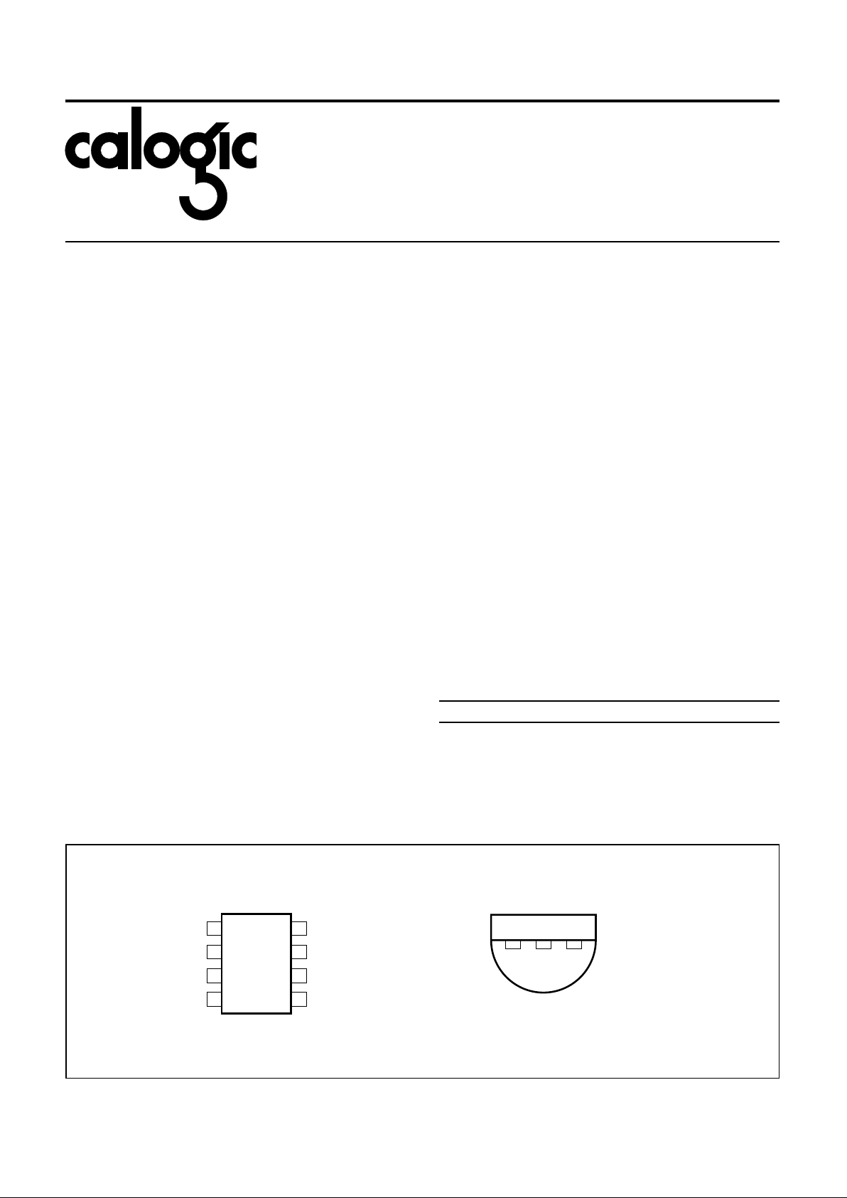
PIN CONNECTIONS
1D-20
123
1. OUTPUT
2. GROUND
3. INPUT
TO-92
BOTTOM VIEW
GROUND
1
2
3
8
7
6
4 5 ERROR
LP2951
1D-19
8-PIN SURFACE MOUNT
5V OR 3.3V TAP
FEEDBACK
INPUT
SHUTDOWN
SENSE
OUTPUT
TOP VIEW
CALOGIC CORPORATION, 237 Whitney Place, Fremont, California 9453 9, Telephone: 510 -656- 2900, FAX: 510-651-3025
Page 2
ABSOLUTE MAXIMUM RATINGS
Power Dissipation . . . . . . . . . . . . . . . . . . . . . Internally Limited
Lead Temp. (Soldering, 5 Seconds) . . . . . . . . . . . . . . . 260
o
C
Storage Tem per atur e Ra nge. . . . . . . . . . . . . . . -65 to +150
o
C
Operating Junct ion Te mper at ure Ra nge
LP2951. . . . . . . . . . . . . . . . . . . . . . . . . . . . . . -55 to +150
o
C
LP2950AC/LP2950C
LP2951AC/LP2951C. . . . . . . . . . . . . . . . . . . -40 to +125
o
C
Input Supply Vo ltag e . . . . . . . . . . . . . . . . . . . . . . -0.3 to +30V
Feedback Input Voltage. . . . . . . . . . . . . . . . . . . . -1.5 to +30V
Shutdown Input Voltage. . . . . . . . . . . . . . . . . . . . -0.3 to +30V
Error Comparator Output. . . . . . . . . . . . . . . . . . . -0.3 to +30V
ESD Rating . . . . . . . . . . . . . . . . . . . . . . . . . . . . . . . . 2KV Min
LP2950 / LP2951
CORPORATION
CALOGIC CORPORATION, 237 Whitney Place, Fremont, California 9453 9, Telephone: 510 -656- 2900, FAX: 510-651-3025
ELECTRICAL CHARACTERISTICS: V
S
= 15V, TA = 25oC, unless otherwise specified .
PARAMETER
LP2951 LP2950AC / LP2951AC LP2950C / LP2951C
UNITS
CONDITIONS
(Note 2)
MIN TYP MAX MIN TYP MAX MIN TYP MAX
3V VERSIONS
Output Voltage
2.985
2.964
3.0 3.015
3.036
2.985
2.970
2.964
3.0
3.0
3.0
3.015
3.030
3.036
2.970
2.955
2.940
3.0
3.0
3.0
3.030
3.045
3.060
V
V
V
TJ = 25oC
-25
o
C ≤ TJ ≤ 85oC
Full Operating T emperature
Output Voltage 2.955 3.0 3.045 2.958 3.0 3.042 2.928 3.0 3.072 V
100µA ≤ I
L
≤ 100mA
T
J
≤T
JMAX
3.3V VERSIONS
Output Voltage
3.284
3.260
3.3 3.317
3.340
3.284
3.267
3.260
3.3
3.3
3.3
3.317
3.333
3.340
3.267
3.251
3.234
3.3
3.3
3.3
3.333
3.350
3.366
V
V
V
T
J
= 25oC
-25
o
C ≤ TJ ≤ 85oC
Full Operating T emperature
Output Voltage 3.251 3.3 3.350 3.254 3.3 3.346 3.221 3.3 3.379 V
100µA ≤ I
L
≤ 100m A
T
J
≤T
JMAX
5V VERSIONS
Output Voltage
4.975
4.94
5.0 5.025
5.06
4.975
4.95
4.94
5.0
5.0
5.0
5.025
5.050
5.06
4.95
4.925
4.90
5.0
5.0
5.0
5.05
5.075
5.10
V
V
V
T
J
= 25oC
-25
o
C ≤ TJ ≤ 85oC
Full Operating T emperature
Output Voltage 4.925 5.0 5.075 4.93 5.0 5.07 4.88 5.0 5.12 V
100µA ≤ I
L
≤ 100m A
T
J
≤ T
JMAX
ALL VOLTAGE OPTIONS
Output Voltage
T emperature Coefficient
20 120 20 50 ppm/
o
C (Note 1)
Line Regulation (Note 3) 0.03 0.1 0.03 0.1 0.04 0.2 % 6V ≤ V
IN
≤ 30V (Note 4)
Load Regulation (Note 3) 0.04 0.1 0.04 0.1 0.1 0.2 % 100µA ≤ I
L
≤ 100m A
Dropout Voltage
(Note 5)
50
38080450
50
38080450
50
38080450mVmV
I
L
= 100µA
I
L
= 100m A
Ground Current
1508170
12
1508170
12
1508170
12
µAmAI
L
= 100µA
I
L
= 100m A
Current Limit 130 200 130 200 130 200 mA V
OUT
= 0
Thermal Regulation 0.05 0.2 0.05 0.2 0.05 0.2 %/W
Output Noise,
10Hz to 100KHz
430
160
100
430
160
100
430
160
100
µVrms
µVrms
µVrms
C
L
= 1µF
C
L
= 200µF
C
L
= 13.3µF
(Bypass = 0.01µF pins 7 to 1 (LP2951))
8-PIN VERSIONS ONLY LP2951 LP2951AC LP2951C
Reference Voltage 1.22 1.235 1.25 1.22 1.235 1.25 1.21 1.235 1.26 V
Reference Voltage 1.19 1.27 1.19 1.27 1.185 1.285 V Over Temperature (Note 6)
Feedback Pin Bias Current 40 60 40 60 40 60 nA
Reference Voltage
T emperature Coefficient
20 20 50 ppm/
o
C (Note 7)
Feedback Pin Bias Current
T emperature Coefficient
0.1 0.1 0.1 nA/
o
C
Page 3
LP2950 / LP2951
CORPORATION
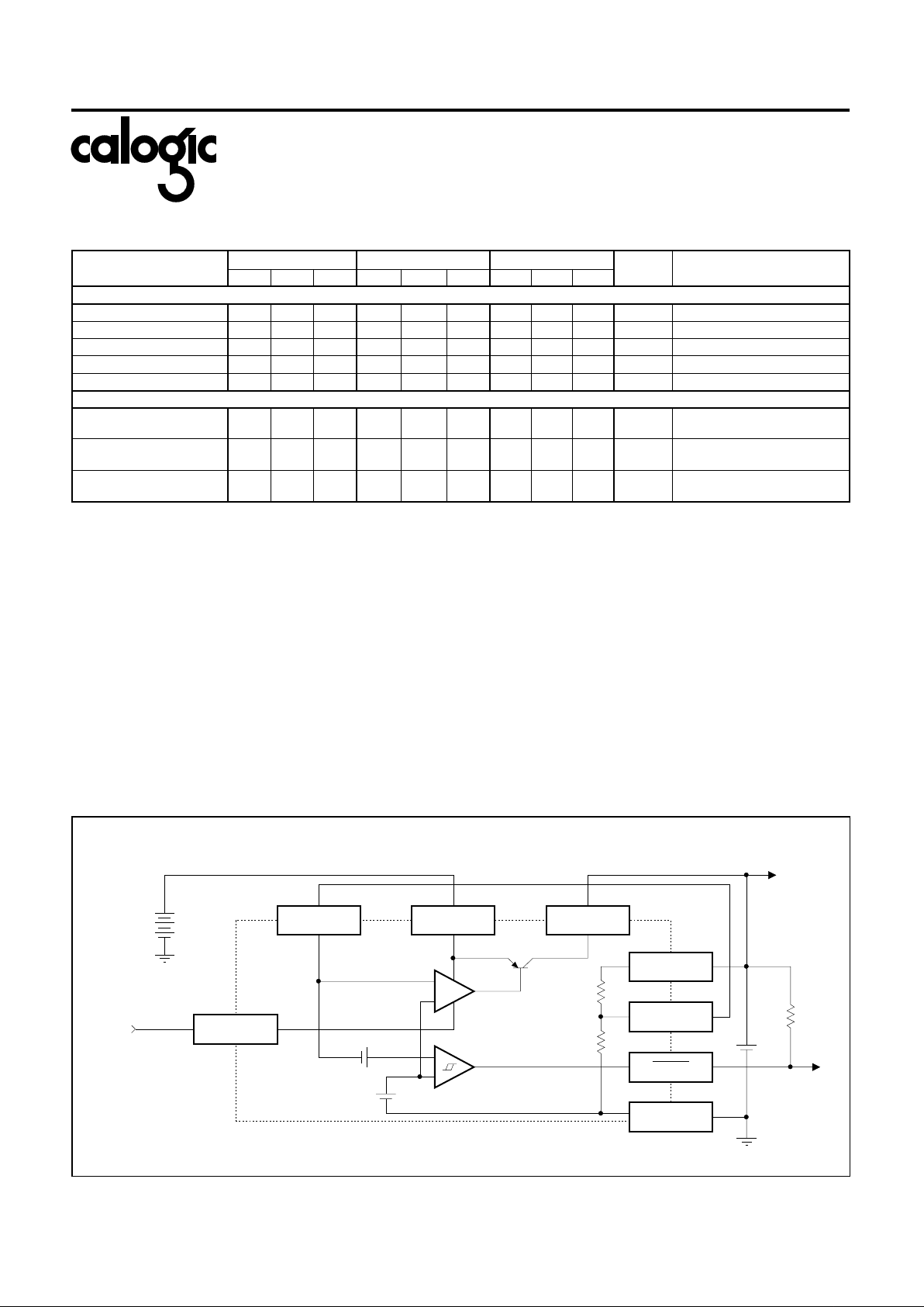
BLOCK DIAGRAM
ERROR DETECTION
COMPARATOR
1D-21
1µF
REFERENCE
1.23V
UNREGULATED DC
ERROR
AMPLIFIER
60mV
+
+
TO CMOS OR
TTL
330kΩ
FROM
CMOS
OR TTL
+
+
5V @ 100mA
MAX
60kΩ
LP2950 AND LP2951 BLOCK DIAGRAM
180kΩ
817
SENSE
6
2
4
5
5V TAP
ERROR
GROUND
INPUT OUTPUTFEEDBACK
SHUTDOWN
3
–
+
–
+
CALOGIC CORPORATION, 237 Whitney Place, Fremont, California 9453 9, Telephone: 510 -656- 2900, FAX: 510-651-3025
ELECTRICAL CHARACTERISTIC S (continued)
PARAMETER
LP2951 LP2950AC / LP2951AC LP2950C / LP2951C
UNITS
CONDITIONS
(Note 2)
MIN TYP MAX MIN TYP MAX MIN TYP MAX
ERROR COMPARATOR
Output Leakage Current 0.01 1 0.01 1 0.01 1 µAV
OH
= 30V
Output Low Voltage 150 250 150 250 150 250 mV V
IN
= 4.5V, IOL = 400µA
Upper Threshold Voltage 40 60 40 60 40 60 mV (Note 7)
Lower Threshold Voltage 75 95 75 95 75 95 mV (Note 7)
Hysteresis 15 15 15 mV (Note 7)
SHUTDOWN INPUT
Inp ut Logic Voltage
2
1.3 0.6
2
1.3 0.7
2
1.3 0.7 V
V
Low (Regulato r ON)
High (Regulator OFF)
Shutdown Pin
Input Current
30
67550800
30
67550800
30
67550800
µAµAV
S
= 2.4V
V
S
= 30V
Regulator Output Current
in Shutdown
310 310 310µA (Note 9)
Note 1: Output or reference voltage temperature coefficients defined as the worst case voltage change divided by the total temperature range.
Note 2: Unless otherwise specified all limits guaranteed for T
J
= 25oC, VIN = 6V, IL=100µA and CL = 1µF. Additional conditions for the 8-pin
versions are feedback tied to 5V tap and output tied to output Sense (V
OUT
= 5V) and V
SHUTDOWN
≤ 0.8V.
Note 3: Regulation is measured at constant junction temperature, using pulse testing with a low duty cycle. Changes in output voltage due to
heating effects are covered under the specification for thermal regulation.
Note 4: Line regulation for the LP2951 is tested at 150
o
C for IL = 1mA. For IL = 100µA and TJ = 125oC, line regulatio n is guara nte ed by desig n to
0.2%. See typical performance characteristics for line regulation versus temperature and load current.
Note 5: Dropout voltage is defined as the input to output differential at which the output voltage drops 100mV below its nominal value measured
at 1V differential at very low values of programmed output voltage, the minimum input supply voltage of 2V (2.3V over temperature) must be
taken input account.
Note 6: V
REF
≤ V
OUT
≤ (VIN - 1V), 2.3 ≤ VIN ≤ 30V, 100µA ≤ IL ≤ 100mA, TJ ≤ T
JMAX
.
Note 7: Comparator thresholds are expressed in terms of a voltage differential at the feedback terminal below the nominal reference voltage
measured at 6V input. To express these thre sh old s in terms of output vo lta ge chan ge , mu ltip l y by the erro r amp lifi er g ai n = V
OUT/VREF
=
(R1+R2)/R2. For example, at a programmed output voltage of 5V, the error output is guaranteed to go low when the output drops by 95 mV x
5V/1.235 = 384mV. Thresho lds remain constant as a percent of V
OUT
as V
OUT
is varied, with the dropout warning occurring at typically 5% below
nominal, 7.5% guaranteed.
Note 8: V
SHUTDOWN
≥ 2V, VIN ≤ 30V, V
OUT
= 0, Feedback pin tied to 5V Tap.
Note 9: All typical values are not guaranteed.
Page 4

APPLICATION HINTS
EXTERNAL CAPACITORS
• The stability of the LP2950/LP2951 requires a 1.0µF or
greater capacitor between output and ground. Oscillation
could occur without this capacitor. Most types of tantalum
or aluminum electrolytic are acceptable. For operations
below -25
o
C a solid tantalum is recommended since the
many aluminum types have electrolytes that freeze at about
-30
o
C. The ESR of about 5Ω or less and resonant
frequency about 500kHz are the most imp orta nt param eter s
in the value of the capacitor. The capacitors value may be
increased without limit .
• At lower values of output current, less output cap acitance is
required for stability. For currents below 10mA the value of
the capacitor can be reduced to 0.33µF and 0.1µF for 1mA.
More output capacitance is needed for the 8-pin version at
voltages below 5V since it runs the error amplifier at lower
gain.
• At worst case 3.3µF or greater must be used for the
condition of 100mA load at 1.23V output.
• The LP2950, unlike other low dropout regulators will remain
stable and in regulation with no load in addition to the
internal voltage divider. This feature is especially important
in applications l ike CMOS RAM keep-alive ci rcuits. When
setting the output voltage of the LP2951 version with
external resistors, a m inimum load of 1µA is r ecommended.
• I f there is more than 10 inches of wire between the input
and the AC filter capacitor or if a battery is used as the input
then a 1µA tantalum or aluminum electrolytic capacitor
should be placed from the input to the ground.
• Instability can occur if there is a stray capacitance to the
LP2951 feedback terminal (pin 7). This could cause more
problems when using a higher value of external resistors to
set the output voltage. This problem can be eliminated by
adding a 100pF capacitor between output and feedback
and increasing the ou tput capacitor t o at least 3.3 µF.
ERROR DETECTION COMP A RATOR OUTPUT
The Comparator produces a logic low output whenever the
LP2951 output falls out of regulatio n by mo re than ar ou nd 5% .
This occurs at approximately 60mV offset divided by the
1.235 reference voltage. This trip level remains 5% below
normal regardless of the programmed output voltage of the
regulator. Figure 1 shows the timing diagram depicting the
ERROR signal and the regulator output voltage as the
LP2951 input is ramped up and down. The ERROR signal
becomes low at around 1.3V input, and goes high around 5V
input (in put v oltage at which V
OUT
= 4.75). Sinc e the LP2951’s
dropout voltage is load dependent, the input voltage trip point
(around 5V) will vary w ith the load cur rent . The outpu t vo ltag e
trip point (appro x. 4.75V) does no t vary with load.
The error comparator has an open-collector output which
requires an external pullup resistor. Depending on the syst em
requirements the resistor may be returned to 5V output or
other supply voltage. In determining the value of this resistor,
note that the output is rated to sink 400µA, this value adds to
battery drain in a low battery condition. Suggested values
range from 100K to 1MΩ. If the output is unused this resistor
is not required.
PROGRAMMING THE OUTPUT VOLTAGE OF LP2951
The LP2951 may be pin-strapped for 5V using its internal
voltage divider by tying Pin 1 (outpu t) to Pin 2 (sense) and Pin
7 (feedback) to Pin 6 (5V Tap). Also, i t may be programmed
for any output voltage between its 1.235V reference and its
30V maximum rating. As seen in Figure 2, an external pair of
resistors is requir ed.
Refer to the equation below for the programm ing of the out put
voltage:
V
OUT
= V
REF
× (1 + R1\R2) + IFBR
1
The V
REF
is 1.235 and IFB is the feedback bias current,
nominally -20nA. The minimum recomme nded load current of
1µA forces an upper limit of 1.2MΩ on value of R
2
. If no load
is presented the I
FB
produces an error of typically 2% in V
OUT
which may be eliminate d at room te mperature by trim m ing R1.
To improve the accuracy choose the value of R2 = 100k this
reduces the error by 0.17% and increases the resistor
program current by 12µA. Since the LP2951 typically draws
60µA at no l oad with Pin 2 open-circuited this is a small price
to pay .
REDUCING OUTPUT NOISE
It may be an advantage to reduce the AC noise present at the
output. One way is to reduce the regulator bandwidth by
increasing the size of the output capacitor. This is the only
way that noise can be reduced on the lead 3 of LP2950, but is
relatively inefficient, as increasing the capacitor from 1µF to
220µF only decreases the noise from 430µV to 160µVrms for
a 100kHz bandwidth at 5V output .
Noise could also be reduced fourfold by a bypass capacitor
across R
1
, since it reduces the high frequency gain from 4 to
unity.
C
BYPASS
≅ 1/2πR1 × 200Hz
or choose 0.01µF. When doing this, the output capacit or must
be increased to 3.3µF to maintain stability. These changes
reduce the output noise from 430µV to 100µVrms for a
100kHz bandwidth at 5V output. With the bypass capacitor
added, noise no longer scales with output voltage so that
improveme nt s are mor e dram at ic at hig her voltages .
LP2950 / LP2951
CORPORATION
CALOGIC CORPORATION, 237 Whitney Place, Fremont, California 9453 9, Telephone: 510 -656- 2900, FAX: 510-651-3025
Page 5

LP2950 / LP2951
CORPORATION
CALOGIC CORPORATION, 237 Whitney Place, Fremont, California 9453 9, Telephone: 510 -656- 2900, FAX: 510-651-3025
LOAD CURRENT (mA)
10
0.01
0.1 100
1D-22
QUIESCENT CURRENT
GROUND PIN CURRENT (mA)
0.1
1
1.0 10
INPUT VOLTAGE (VOLTS)
250
0
010
1D-24
INPUT CURRENT
INPUT CURRENT (µA)
5 6 7 84 9321
25
50
75
100
125
150
175
200
225
=
RL= 50kΩ
∞
R
L
5V OUTPUT
INPUT VOLTAGE (VOLTS)
6
0
3
06
1D-23
DROPOUT
CHARACTERISTICS
3
OUTPUT VOLTAGE (VOLTS)
12 45
1
2
4
5
RL= 50kΩ
R
L
= 50Ω
5V OUTPUT
TYPICAL PERFORMANCE CHARACTERI STIC S
INPUT VOLTAGE (VOLTS)
120
0
010
1D-25
INPUT CURRENT
INPUT CURRENT (mA)
5 6 7 84 9321
60
20
40
80
100
10
70
30
50
90
110
RL= 50Ω
5V OUTPUT
INPUT VOLTAGE (VOLTS)
160
0
08
1D-27
QUIESCENT CURRENT
QUIESCENT CURRENT (µA)
1 2 3 4 5 6 7
20
40
60
100
120
140
80
5V OUTPUT
IL= 1mA
I
L
= 0
TEMPERATURE (˚C)
5.06
4.94
5.0
–75 150
1D-26
OUTPUT VOLTAGE vs
TEMPERATURE OF 3
REPRESENTATIVE UNITS
OUTPUT VOLTAGE (V)
4.96
4.98
5.02
5.04
–50 –25 0 25 50 75 100 125
5V OUTPUT
0.2%
TEMPERATURE (˚C)
170
100
–75 150
1D-28
SHORT CIRCUIT CURRENT
SHORT CIRCUIT CURRENT (mA)
–50 –25 0 25 50 75 100 125
160
150
140
130
120
110
OUTPUT CURRENT
500
0
100µA 100mA
1D-30
DROPOUT VOLTAGE
DROPOUT VOLTAGE (mV)
400
300
200
100
10mA1mA
TJ= 25˚C
TEMPERATURE (˚C)
600
0
–75 150
1D-29
DROPOUT VOLTAGE
DROPOUT VOLTAGE (mV)
–50 –25 0 25 50 75 100 125
500
400
300
100
50
IL= 100mA
I
L
= 100µA
TEMPERATURE (˚C)
120
50
–75 150
1D-31
QUIESCENT CURRENT
QUIESCENT CURRENT (µA)
–50 –25 0 25 50 75 100 125
110
100
90
80
70
60
5V OUTPUT
V
IN
= 6V
I
L
= 100µA
INPUT VOLTAGE (V)
8
0
08
1D-33
QUIESCENT CURRENT
QUIESCENT CURRENT (mA)
1 2 3 4 5 6 7
1
2
3
5
6
7
4
IL= 100mA
5V OUTPUT
TEMPERATURE (˚C)
10
7
–75 150
1D-32
QUIESCENT CURRENT
QUIESCENT CURRENT (mA)
–50 –25 0 25 50 75 100 125
9
8
5V OUTPUT
VIN= 6V
I
L
= 100mA
Page 6

LP2950 / LP2951
CORPORATION
CALOGIC CORPORATION, 237 Whitney Place, Fremont, California 9453 9, Telephone: 510 -656- 2900, FAX: 510-651-3025
TEMPERATURE (˚C)
2.2
1.6
–75 150
1D-34
LP2951 MINIMUM
OPERATING VOLTAGE
MINIMUM OPERATING VOLTAGE (V)
–50 –25 0 25 50 75 100 125
2.0
1.8
1.7
2.1
1.9
FEEDBACK VOLTAGE (V)
50
–250
–2.0 1.0
1D-36
LP2951 FEEDBACK
PIN CURRENT
FEEDBACK CURRENT (µA)
–100
–150
–200
–1.5 –1.0 0.50–0.5
–50
0
TA= 125˚C
T
A
= –55˚C
PIN 7 DRIVEN BY
EXTERNAL SOURCE
(REGULATROR RUN
OPEN LOOP)
TA= 25˚C
TEMPERATURE (˚C)
20
–30
–75 150
1D-35
LP2951 FEEDBACK
BIAS CURRENT
BIAS CURRENT (nA)
–50 –25 0 25 50 75 100 125
10
0
–10
–20
INPUT VOLTAGE (V)
8
–2
5
1D-37
LP2951 ERROR
COMPARATOR OUTPUT
COMPARATOR OUTPUT (V)
6
4
2
0
4
3210
V
OUT
= 5V
NOTE: PULLUP RESISTOR
TO SEPARATE 5V SUPPLY
HYSTERESIS
TIME (µs)
100mV
4V
800
1D-39
LINE TRANSIENT
RESPONSE
INPUT
VOLTAGE
0 200 400 600
0
8V
6V
50mV
–50mV
OUTPUT VOLTAGE
CHANGE
IL= 1mA
V
OUT
= 5V
C
L
= 1µA
OUTPUT LOW VOLTAGE (V)
2.5
0.0
0.0 0.9
1D-38
LP2951 COMPARATOR
SINK CURRENT
SINK CURRENT (mA)
0.1 0.2 0.3 0.4 0.5 0.6 0.7 0.8
2.0
1.5
1.0
0.5
TA= 125˚C
T
A
= 25˚C
T
A
= –55˚C
TYPICAL PERFORMANCE CHARACTERI STICS ( cont inue d)
FREQUENCY (Hz)
10
0.01
10 1M
OUTPUT IMPEDANCE
OUTPUT IMPEDANCE (OHMS)
100 1K 100K10K
0.1
1
0.02
0.05
0.2
0.5
2
5
1D-40
IO= 100µA
I
O
= 1mA IO= 100mA
V
OUT
= 5V
C
L
= 1µA
FREQUENCY (Hz)
90
20
1D-42
RIPPLE REJECTION
RIPPLE REJECTION (dB)
80
70
60
50
40
30
10
6
10
5
10
4
10
3
10
2
10
1
IL= 1mA
IL= 10mA
V
OUT
CL= 1µF
V
IN
= 6V
= 5V
FREQUENCY (Hz)
90
20
1D-41
RIPPLE REJECTION
RIPPLE REJECTION (dB)
80
70
60
50
40
30
10
6
10
5
10
4
10
3
10
2
10
1
IL= 0
I
L
= 100µA
V
OUT
= 5V
V
IN
= 6V
CL= 1µF
TIME (ms)
250
100µA
5
1D-43
LOAD TRANISENT
RESPONSE
LOAD CURRENT
50
100mA
150
OUTPUT VOLTAGE
CHANGE (mV)
43210
200
100
0
–50
–100
CL= 1µF
V
OUT
= 5V
TIME (µs)
1D-45
LP2951
ENABLE TRANSIENT
SHUTDOWN
PIN VOLTAGE (V)
OUTPUT
VOLTAGE (V)
–100 7000 100 200 300 400 500 600
7
–2
0
2
0
1
2
3
4
5
6
CL= 1µF
I
L
= 10mA
V
IN
= 8V
V
OUT
= 5VCL= 10µF
TIME (ms)
80
100µA
20
1D-44
LOAD TRANSIENT
RESPONSE
LOAD CURRENT
0
100mA
40
OUTPUT VOLTAGE
CHANGE (mV)
1612840
60
20
–20
–40
–60
OUT
CL= 10µF
V = 5V
Page 7

LP2950 / LP2951
CORPORATION
CALOGIC CORPORATION, 237 Whitney Place, Fremont, California 9453 9, Telephone: 510 -656- 2900, FAX: 510-651-3025
TYPICAL APPLICA TION S
1F-44
*SEE APPLICATION INFO.
OUTPUT
VOLTAGE
INPUT
VOLTAGE
4.75V
ERROR*
1.3V
5.0V
R
1
+V
IN
LP2951
FB
4
1F-45
SD
GND
V
OUT
7
ERROR
8
1
3
R
2
ERROR
OUTPUT
SHUTDOWN
INPUT
3.3µF
+
+V
IN
1.2 TO 30V
1.23V
.01µF
100K
5
V
REF
R
1
+V
IN
LP2951
FB
4
1F-46
SD
GND
V
OUT
7
ERROR
8
1
+V
IN
1µF
+
3
V
OUT
470KΩ
470KΩ
R
2
LATCH OFF WHEN ERROR FLAG OCCURS
5
*V
OUT
= V
IN
+V
IN
LP2951
FB
4
1F-47
SD
GND
V
OUT
7
ERROR
OUTPUT
SHUTDOWN
INPUT
ERROR
8
1
+V
IN
*MINIMUM INPUT - OUTPUT VOLTAGE RANGES FROM 4mV TO 400mV.
DEPENDING ON LOAD CURRENT. CURRENT LIMIT IS TYPICALLY 160mA.
WIDE INPUT VOLTAGE RANGE CURRENT LIMITER
5
3
FIGURE 1. ERROR OUTPUT TIMING FIGURE 2. ADJUSTABLE REG ULATOR
Page 8

CALOGIC CORPORATION, 237 Whitney Place, Fremont, California 9453 9, Telephone: 510 -656- 2900, FAX: 510-651-3025
LP2950 / LP2951
CORPORATION
TYPICAL APPLICA T IONS (continue d)
LP2951
4
1G-24
GND
8
1
3
SENSE
MAIN V-
MEMORY V+
NI-CAD
BACKUP
BATTERY
CLM385
6V
SEALED
LEADACID
BATTERY
SOURCE
100KΩ
1.5KΩ120KΩ
400KΩ
20KΩ
FB
IN457
SD
V
OUT
+V
IN
FOR 5.5V
LOW BATTERY DISCONNECT
+
1µF
+
+V
IN
LP2951
TAP
4
1G-25
SD
GND
V
OUT
6
ERROR
8
1
1µF
+
3
+V
OUT
39k
Ω
100k
Ω
100k
Ω
100k
Ω
–
+
C4
2
SENSE
= 5V
7
39k
Ω
100k
Ω
1k
Ω
1k
Ω
10k
Ω
20k
Ω
<6.2V**
<6.0V**
<5.8V**
1%
1%
1%
1%
5
R
3
6V
LEADACID
BATTERY
REGULATOR WITH STATE-OF-CHARGE INDICATOR
RESET
–
+
C1
–
+
C2
–
+
C3
*OPTIONAL LATCH OFF WHEN DROPOUT OCCURS. ADJUST R3 FOR C2 SWITCHING WHEN V IS 6.0V.
**OUTPUTS GO LOW WHEN V DROPS BELOW DESIGNATED THRESHHOLDS.
IN
IN
Page 9

CALOGIC CORPORATION, 237 Whitney Place, Fremont, California 9453 9, Telephone: 510 -656- 2900, FAX: 510-651-3025
LP2950 / LP2951
CORPORATION
TYPICAL APPLICA T IONS (continue d)
+V
IN
LP2951
FB
4
1F-48
GND
8
5
SYSTEM OVER TEMPERATURE PROTECTION CIRCUIT
AUX SHUTDOWN
INPUT
+V
IN
AS35
5 DEGREE SHUTDOWN FLAG
V
OUT
1
EXTERNAL CIRCUIT
PROTECTED FROM
OVER TEMPERATURE
(V+ GOES OFF WHEN
TEMP > 125)
OR
TEMP
SENSOR
7
+
–
3
ERROR
SD
10KΩ
ON
OFF
RELAY
8.2KΩ
LP2951
4
1F-49
GND
8
1
OPEN CIRCUIT DETECTOR FOR 4mA TO 20mA CURRENT LOOP
7
FB 2
4 20mA
IN4001
360KΩ
0.1µF
IN457
OUTPUT
4.7mA
+5v
MIN VOLTAGE = 4V
+V
IN
V
OUT
LP2951
4.7µF
LOAD 50mA
TO 300mA
OUTPUT
5V
1
2
SENSE
GND
5
UNREGULATED INPUT
3
300mA REGULATOR WITH 0.75 DROPOUT
74
2N5432
27KΩ
330KΩ
IN
1F-50
V
TAP
FB
V
OUT
+
Page 10

CALOGIC CORPORATION, 237 Whitney Place, Fremont, California 9453 9, Telephone: 510 -656- 2900, FAX: 510-651-3025
LP2950 / LP2951
CORPORATION
SCHEMAT IC DIAGRAM
GND
SHDN
5V TAP
SENSE
OUT
FEEDBACKIN
R25
2.8
k
Ω
R23 60k
Ω
R21 8
Ω
R24
50k
Ω
R16
30k
Ω
R15
100k
Ω
R17
10
Ω
R13
100
k
Ω
R14
350
k
Ω
R22
150k
Ω
R17
12k
Ω
R28
60k
Ω
R27
182k
Ω
R18
20k
Ω
R26
60k
Ω
R3
50k
Ω
R4
13k
Ω
R30
30k
Ω
R5
180
k
Ω
R6
140
k
Ω
R9
27.8k
Ω
R2
50k
Ω
R1
20k
Ω
R8
31.4k
Ω
R10
150
k
Ω
R12
110
k
Ω
R11
18
k
Ω
R11
20.6
k
Ω
Q1
Q30 Q31
Q19Q18
Q29
Q28
Q22
Q21
Q20
Q34
Q40
Q41
Q42
Q13 Q12
Q3 Q4
Q7
Q8
Q9
Q6
Q15A Q15B
Q16 Q17
Q14
Q25
Q24
Q23
Q11
Q38
Q37 Q36
Q39
Q26
Q2
Q5
C1
20pF
C2
40pF
1G-01
10
4
2
5
6
3
4
1
2
1
2
3
3
24
ERROR
— — — DENOTES CONNECTION ON LP2950 ONLY
 Loading...