

Page 1
Product Specification
SPECIFICATION
LP154WU1
Liquid Crystal Display
FOR
APPROVAL
)
(
(
Preliminary Specification
◆
)
Final Specification
www.jxlcd.com
15.4” WUXGA TFT LCDTitle
DELLCustomer
LP154WU1-TLA1MODEL
*When you obtain standard approval,
www.jxlcd.com
please use the above model name without suffix
LG.Philips LCD Co., Ltd.SUPPLIER
LP154WU1*MODEL
TLA1Suffix
SIGNATUREAPPROVED BY
/
/
/
Please return 1 copy for your confirmation with
your signature and comments.
Ver. 1.2 Sep. 29, 2007
APPROVED BY
S.C. Yoon / G.Manager
REVIEWED BY
Y.S.Ha / Manager
/ Manager
PREPARED BY
P.A.Choi / Engineer
/ Engineer
Products Engineering Dept.
LG. Philips LCD Co., Ltd
SIGNATURE
1 / 32
Page 2
Product Specification
Contents
LP154WU1
Liquid Crystal Display
ITEMNo
COVER
CONTENTS
RECORD OF REVISIONS
GENERAL DESCRIPTION1
ABSOLUTE MAXIMUM RATINGS2
ELECTRICAL SPECIFICATIONS3
ELECTRICAL CHARACTREISTICS 3-1
INTERFACE CONNECTIONS 3-2
SIGNAL TIMING SPECIFICATIONS 3-3
SIGNAL TIMING WAVEFORMS 3-4
COLOR INPUT DATA REFERNECE 3-5
www.jxlcd.com
www.jxlcd.com
POWER SEQUENCE 3-6
OPTICAL SFECIFICATIONS4
MECHANICAL CHARACTERISTICS5
Page
1
2
3
4
5
6
8
12
12
13
14
15
18
RELIABLITY6
INTERNATIONAL STANDARDS7
SAFETY 7-1
EMC 7-2
PACKING8
DESIGNATION OF LOT MARK 8-1
PACKING FORM 8-2
PRECAUTIONS9
APPENDIX. Enhanced Extended Display Identification Data A
Ver. 1.2 Sep. 29, 2007
25
26
26
26
27
27
27
28
30
2 / 32
Page 3
Product Specification
RECORD OF REVISIONS
LP154WU1
Liquid Crystal Display
DescriptionPageRevision DateRevision No
First Draft.Feb.8.20071.0
Dclk FrequencyApril.16.20071.1
EDID Update (Dclk Frequency)Sep.21.20071.2
www.jxlcd.com
www.jxlcd.com
EDID
ver
0.3
0.3
0.4
Ver. 1.2 Sep. 29, 2007
3 / 32
Page 4
LP154WU1
Liquid Crystal Display
Product Specification
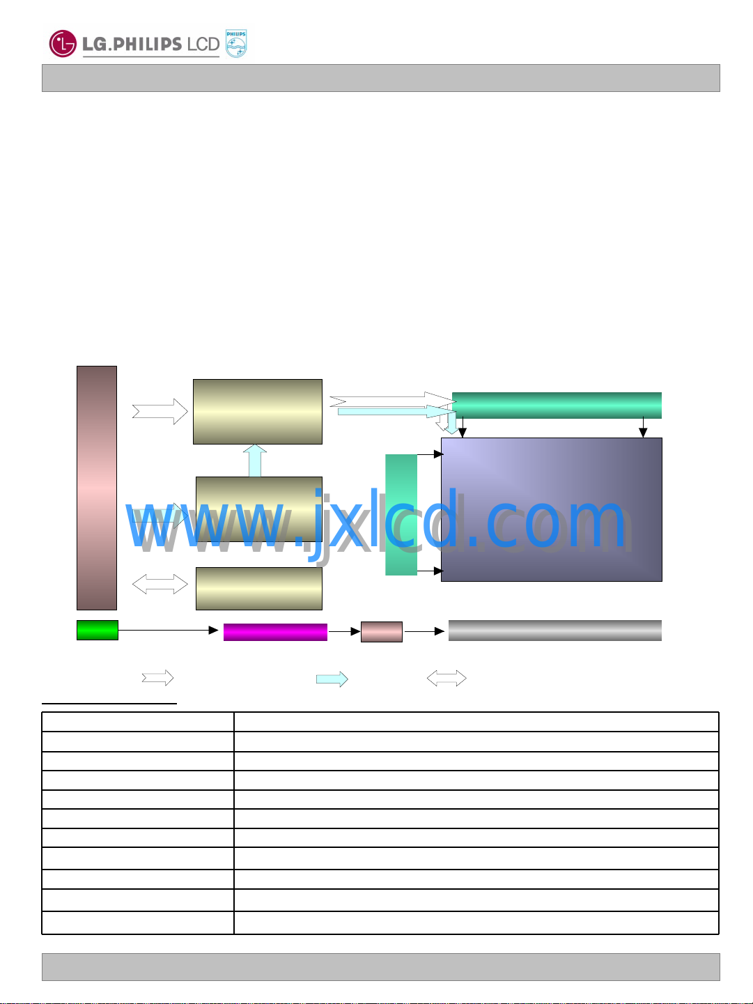
1. General Description
The LP154WU1 is a Color Active Matrix Liquid Crystal Display with an integral Cold Cathode Fluorescent
Lamp (CCFL) backlight system. The matrix employs a-Si Thin Film Transistor as the active element. It is a
transmissive type display operating in the normally white mode. This TFT-LCD has 15.4 inches diagonally
measured active display area with WXGA resolution(1200 vertical by 1920 horizontal pixel array). Each pixel
is divided into Red, Green and Blue sub-pixels or dots which are arranged in vertical stripes. Gray scale or
the brightness of the sub-pixel color is determined with a 6-bit gray scale signal for each dot, thus, presenting
a palette of more than 262,144 colors.
The LP154WU1 has been designed to apply the interface method that enables low power, high speed, low
EMI.
The LP154WU1 is intended to support applications where thin thickness, low power are critical factors and
graphic displays are important. In combination with the vertical arrangement of the sub-pixels, the
LP154WU1 characteristics provide an excellent flat display for office automation products such as Notebook
PC.
CN1 User connector 30 Pin
www.jxlcd.com
www.jxlcd.com
J1
General Features
LVDS &
Timing
Control
Block
POWE
R
BLOCK
EDID
BLOCK
Inverter
Control & Data Power EDID signal & Power
15.4 inches diagonal Active Screen Size
344.0 (H) × 222.0 (V) × 6.5(D, max) mmOutline Dimension
0.1725 mm × 0. 1725 mm Pixel Pitch
1920 horiz. by 1200 vert. Pixels RGB strip arrangementPixel Format
6-bit, 262,144 colorsColor Depth
210 cd/m2(Typ.) , 5 pointLuminance, White
Total 6.27 Watt(Typ.) @ LCM circuit 1.85 Watt(Typ.), B/L input 4.42 Watt(Typ.)Power Consumption
575 g (Max.) without inverter & bracketWeight
Transmissive mode, normally whiteDisplay Operating Mode
Anti-glare treatment of the front polarizerSurface Treatment
YesRoHS Comply
(LOG_B type)
CN2
1
Gate Driver
1200
Source Driver Circuit
1 1920
TFT-LCD Panel
(1920 x 1200)
Backlight Ass’y
Ver. 1.2 Sep. 29, 2007
4 / 32
Page 5
LP154WU1
Liquid Crystal Display
Product Specification
2. Absolute Maximum Ratings
The following are maximum values which, if exceeded, may cause faulty operation or damage to the unit.
Table 1. ABSOLUTE MAXIMUM RATINGS
Parameter Notes
Power Input Voltage
Operating Temperature
Storage Temperature
Operating Ambient Humidity
Storage Humidity
Note : 1. Temperature and relative humidity range are shown in the figure below.
Wet bulb temperature should be 39C Max, and no condensation of water.
www.jxlcd.com
www.jxlcd.com
Wet Bulb
Temperature [℃]
20
10
0
Symbol
60
50
40
30
Values
MaxMin
90% 80%
60%
40%
20%
10%
Units
Humidity[(%)RH]
Storage
Operation
at 25 5CVdc4.0-0.3VCC
1C500TOP
1C60-20HST
1%RH9010HOP
1%RH9010HST
-20
Ver. 1.2 Sep. 29, 2007
10
20 30 40 50
Dry Bulb Temperature [℃]
60 70 800
5 / 32
Page 6
LP154WU1
Liquid Crystal Display
Product Specification
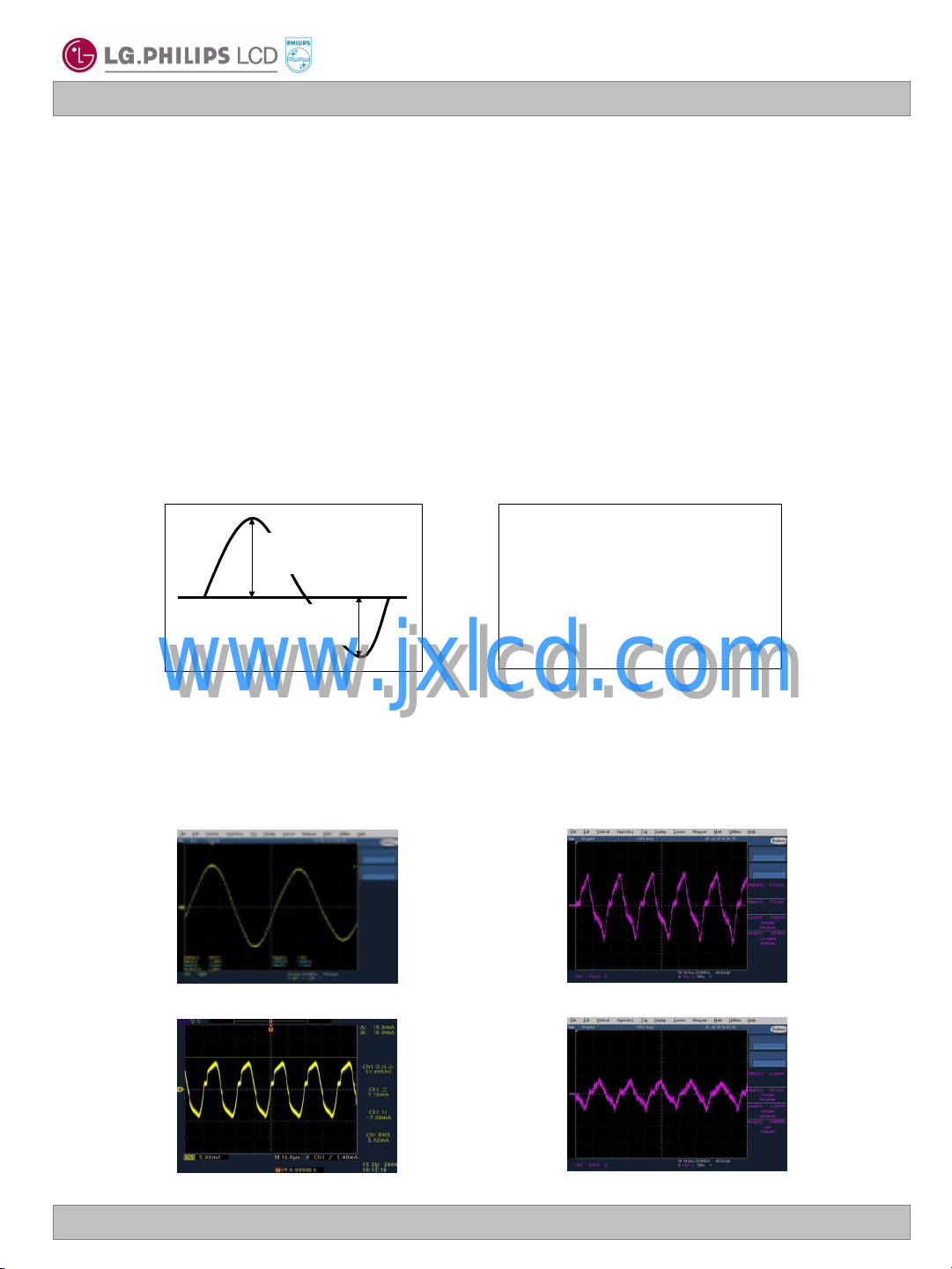
3. Electrical Specifications
3-1. Electrical Characteristics
The LP154WU1 requires two power inputs. One is employed to power the LCD electronics and to drive the
TFT array and liquid crystal. The second input which powers the CCFL, is typically generated by an
inverter. The inverter is an external unit to the LCD.
Table 2. ELECTRICAL CHARACTERISTICS
Parameter Symbol
MODULE :
Power Supply Input Current
LAMP :
Operating Voltage
Operating Current
Power Consumption
Operating Frequency
www.jxlcd.com
www.jxlcd.com
Mosaic 1mA640560480
I
CC
BL
BL
BL
BL
Values
DC
RMS
RMS
NotesUnit
1Watt2.121.851.58Pc Power Consumption
2Ohm11010090Zm Differential Impedance
3mA
4Min3--Ts Discharge Stabilization Time
5Hrs--12,000 Life Time
MaxTypMin
3.63.33.0VCC Power Supply Input Voltage
835(3.0mA)680(6.5mA)665(7.0mA)V
7.06.53.0I
4.64.2-P
V
V
kHz806045f
Established Starting Voltage
at 25℃
at 0 ℃
Note)
1. The specified current and power consumption are under the Vcc = 3.3V , 25℃, fv = 60Hz condition
whereas Mosaic pattern is displayed and fv is the frame frequency.
2. This impedance value is needed to proper display and measured form LVDS Tx to the mating connector.
3. The typical operating current is for the typical surface luminance (LWH) in optical characteristics.
4. Define the brightness of the lamp after being lighted for 5 minutes as 100%, Ts is the time required for
the brightness of the center of the lamp to be not less than 95%.
5. The life time is determined as the time at which brightness of lamp is 50% compare to that of initial value
at the typical lamp current.
Ver. 1.2 Sep. 29, 2007
Vs
1200
1500
V
RMS
V
RMS
6 / 32
Page 7
LP154WU1
Liquid Crystal Display
Product Specification
Note)
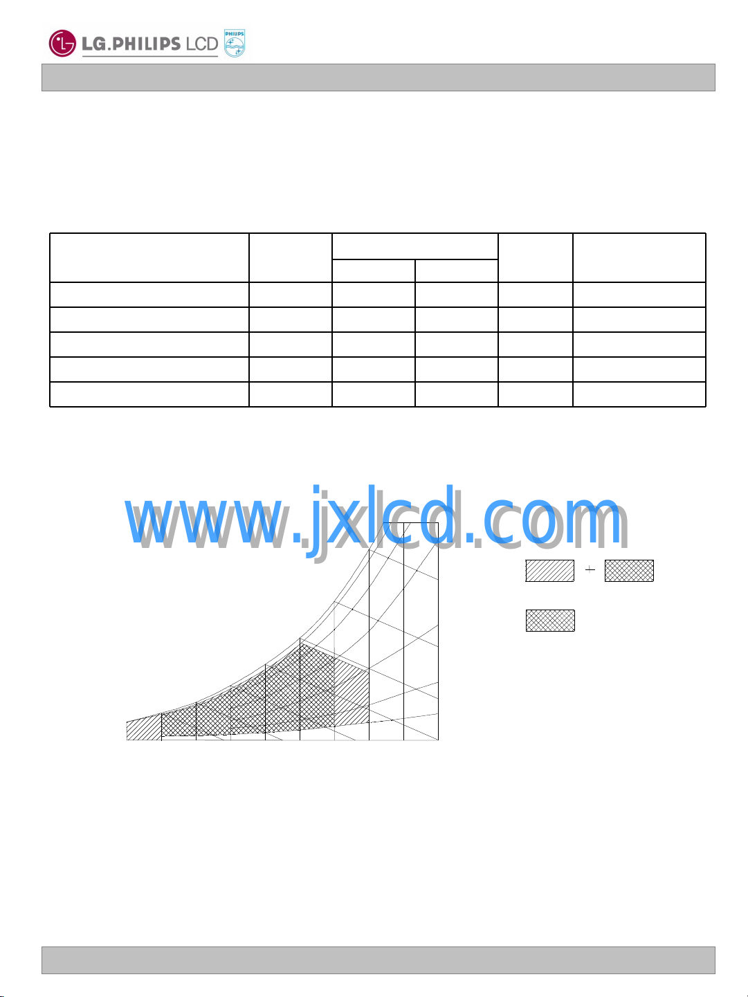
6. The output of the inverter must have symmetrical(negative and positive) voltage waveform and
symmetrical current waveform.(Asymmetrical ratio is less than 10%) Please do not use the inverter
which has asymmetrical voltage and asymmetrical current and spike wave.
Lamp frequency may produce interface with horizontal synchronous frequency and as a result this may
cause beat on the display. Therefore lamp frequency shall be as away possible from the
horizontal synchronous frequency and from its harmonics in order to prevent interference.
7. It is defined the brightness of the lamp after being lighted for 5 minutes as 100%.
TS is the time required for the brightness of the center of the lamp to be not less than 95%.
8. The lamp power consumption shown above does not include loss of external inverter.
The applied lamp current is a typical one.
9. Requirements for a system inverter design, which is intended to have a better display performance, a
better power efficiency and a more reliable lamp, are following.
It shall help increase the lamp lifetime and reduce leakage current.
a. The asymmetry rate of the inverter waveform should be less than 10%.
b. The distortion rate of the waveform should be within √2 ±10%.
* Inverter output waveform had better be more similar to ideal sine wave.
* Asymmetry rate:
I p
| I p – I –p | / I
* 100%
rms
10. Inverter open voltage must be more than lamp voltage for more than 1 second for start-up.
Otherwise, the lamps may not be turned on.
※ Do not attach a conducting tape to lamp connecting wire.
If the lamp wire attach to a conducting tape, TFT-LCD Module has a low luminance and the inverter
has abnormal action. Because leakage current is occurred between lamp wire and conducting tape.
Ex of current wave)
www.jxlcd.com
www.jxlcd.com
Normal current wave - Standard
I -p
* Distortion rate
I p (or I –p) / I
Abnormal current wave - Bad
rms
Abnormal current wave - Bad
Ver. 1.2 Sep. 29, 2007
Abnormal current wave - Bad
7 / 32
Page 8
LP154WU1
Liquid Crystal Display
Product Specification
3-2. Interface Connections
This LCD employs two interface connections, a 30 pin connector is used for the module electronics interface
and the other connector is used for the integral backlight system.
The electronics interface connector is a model GT101-30S-HR11 manufactured by LSC.
Table 3. MODULE CONNECTOR PIN CONFIGURATION (CN1)
NotesDescriptionSymbolPin
GroundGND1
Power Supply, 3.3V Typ.VCC2
Power Supply, 3.3V Typ.VCC3
1, Interface chips
1.1 LCD : SW0610_M(LCD Controller)
including LVDS Receiver
1.2 System : THC63LVD823A or equivalent
* Pin to Pin compatible with THINE LVDS
2. Connector
2.1 LCD : MDF76LBRW-30S-1H (HIROSE)
or
its compatibles
2.2 Mating : FI-X30M or equivalent.
2.3 Connector pin arrangement
30
[LCD Module Rear View]
1
10
11
12
13
14
15
16
17
18
19
20
21
22
23
24
25
26
27
28
29
30
4
5
6
7
8
9
www.jxlcd.com
www.jxlcd.com
RA2+ Even channel differential data input
DDC 3.3V powerV EEDID
Reserved for supplier test pointNC
DDC ClockClk EEDID
DDC DataDATA EEDID
Odd channel differential data inputRIN 0-
Odd channel differential data inputRIN 0+
GroundGND
Odd channel differential data inputRIN 1-
Odd channel differential data inputRIN 1+
GroundGND
Odd channel differential data inputRIN 2-
Odd channel differential data inputRIN 2+
GroundGND
Odd channel differential clock inputCLKIN-
Odd channel differential clock inputCLKIN+
GroundGND
Even channel differential data inputRA2-
GroundGND
Even channel differential data inputRB2-
Even channel differential data inputRB2+
GroundGND
Even channel differential data inputRC2-
Even channel differential data inputRC2+
GroundGND
Even channel differential clock inputRCLK2-
Even channel differential clock inputRCLK2+
The backlight interface connector is a model BHSR-02VS-1, manufactured by JST or Compatible.
The mating connector part number is SM02B-BHSS-1 or equivalent.
PIN1
PIN2PIN2
Table 4. BACKLIGHT CONNECTOR PIN CONFIGURATION (J3)
NotesDescriptionSymbolPin
1Power supply for lamp (High voltage side)HV1
1Power supply for lamp (Low voltage side)LV2
Notes : 1. The high voltage side terminal is colored black and the low voltage side terminal is white.
Ver. 1.2 Sep. 29, 2007
8 / 32
Page 9
Product Specification
LVDS +
LVDS -
0V
V
CM
# |VID| = |(LVDS +) – (LVDS -)|
# VCM= {(LVDS +) + ( LVDS -)}/2
|VID|
V
IN_MAXVIN_MIN
LVDS Data
t
SKEW
LVDS Clock
T
clk
t
SKEW (Fclk
= 1/T
clk
)
1) 85MHz > Fclk ≥ 65MHz : -400 ~ +400
2) 65MHz > Fclk ≥ 25MHz : -600 ~ +600
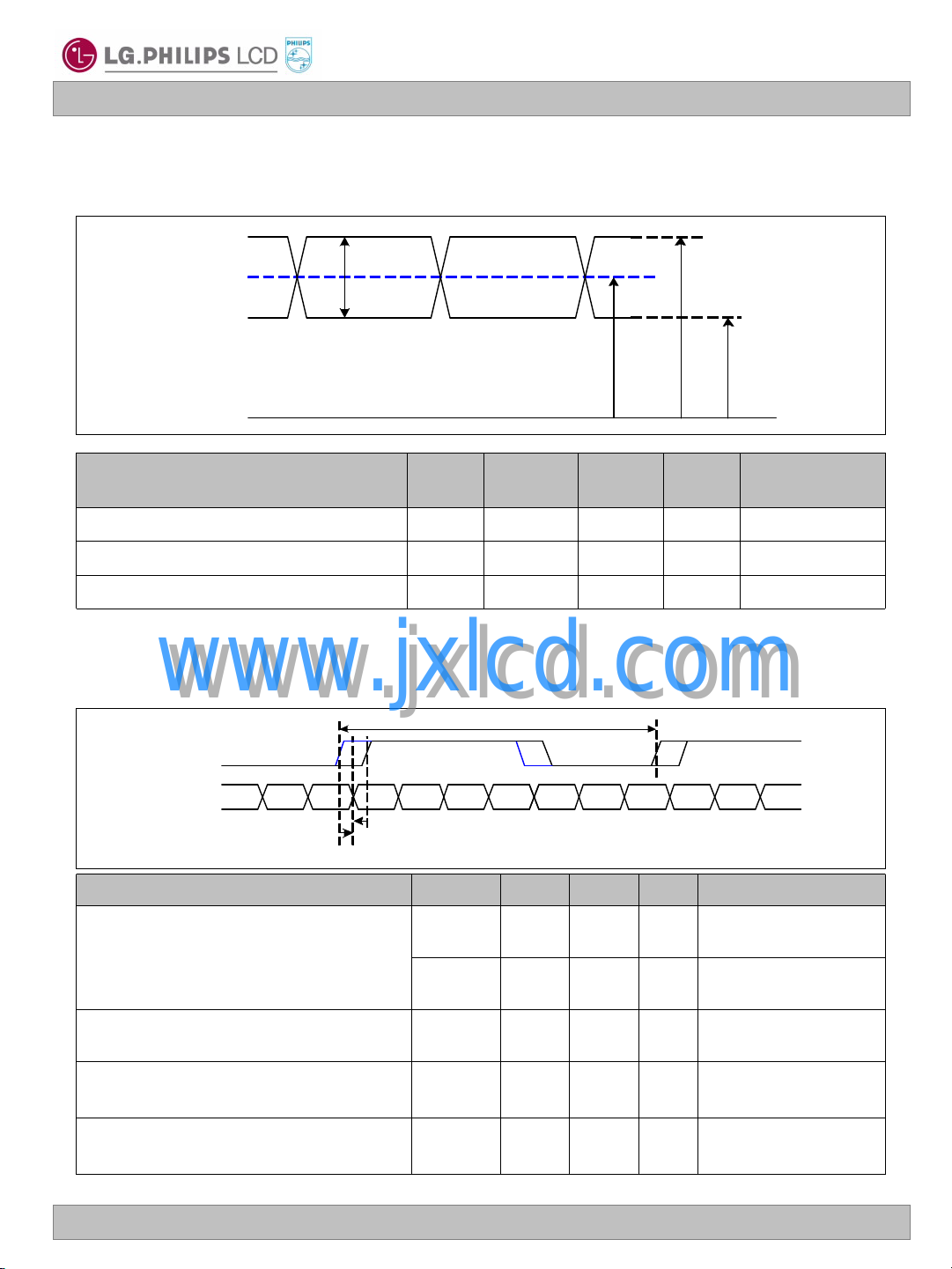
3-3. LVDS Signal Timing Specifications
3-3-1. DC Specification
LP154WU1
Liquid Crystal Display
Description
LVDS Common mode Voltage
LVDS Input Voltage Range
3-3-2. AC Specification
www.jxlcd.com
www.jxlcd.com
LVDS Clock to Data Skew Margin
Symbo
l
CM
IN
SKEW
SKEW
NotesUnitMaxMin
-mV600100|VID|LVDS Differential Voltage
-V1.80.6V
-V2.10.3V
NotesUnitMaxMinSymbolDescription
ps+ 400 400-t
600-
ps+ 600t
85MHz > Fclk ≥
65MHz
65MHz > Fclk ≥
25MHz
LVDS Clock to Clock Skew Margin (Even
to Odd)
Maximum deviation
of input clock frequency during SSC
Maximum modulation frequency
of input clock during SSC
Ver. 1.2 Sep. 29, 2007
SKEW_EO
DEV
MOD
- 1/7
+ 1/7t
T
clk
%± 3-F
KHz200-F
-
-
-
9 / 32
Page 10
LVDS Even Data
LVDS Odd Clock
LVDS Even Clock
t
SKEW_EO
T
clk
T
clk
OG0 OR5 OR4 OR3 OR2 OR1 OR0
OB1 OB0 OG5 OG4 OG3 OG2 OG1
DE VSYNC HSYNC OB5 OB4 OB3 OB2
X OB7 OB6 OG7 OG6 OR7 OR6
Current(Nth) CyclePrevious(N-1)th Cycle Next(N+1)th Cycle
RCLK +
RXinO0 +/-
Tclk * 4/7 Tclk * 3/7
Tclk
Tclk * 1/7
MSB R7
R6
R5
R4
R3
R2
R1
R0LSB
EG0 ER5 ER4 ER3 ER2 ER1 ER0
EB1 EB0 EG5 EG4 EG3 EG2 EG1
DE
VSYNC HSYNC
EB5 EB4 EB3 EB2
X EB7 EB6 EG7 EG6 ER7 ER6
* ODD = 1st Pixel
EVEN = 2nd Pixel
RXinO1 +/-
RXinO2 +/-
RXinO3 +/-
RXinE0 +/-
RXinE1 +/-
RXinE2 +/-
RXinE3 +/-
OR3 OR2 OR1 OR0
OG4 OG3 OG2 OG1
OB5 OB4 OB3 OB2
OG7 OG6 OR7 OR6
ER3 ER2 ER1 ER0
EG4 EG3 EG2 EG1
EB5 EB4 EB3 EB2
EG7 EG6 ER7 ER6
OG0 OR5 OR4
OB1 OB0 OG5
DE VSYNC HSYNC
X OB7 OB6
EG0 ER5 ER4
EB1 EB0 EG5
DE
VSYNC HSYNC
X EB7 EB6
Freq.
F
max
F
center
F
min
Product Specification
< Clock skew margin between channel >
LP154WU1
Liquid Crystal Display
F
* F
center
DEV
3-3-3. Data Format
1) LVDS 2 Port
Ver. 1.2 Sep. 29, 2007
www.jxlcd.com
www.jxlcd.com
< Spread Spectrum >
< LVDS Data Format >
1
F
MOD
Time
10 / 32
Page 11

2) LVDS 1 Port
RCLK+
LP154WU1
Liquid Crystal Display
Product Specification
RA+/-
RB+/-
RC+/-
RD+/-
R3 R2
G4 G3
B5 B4
G7 G6
Previous (N-1)th Cycle Next(N+1)th Cycle
www.jxlcd.com
www.jxlcd.com
R1 R0
G2 G1
B3 B2
R7 R6
G0 R5 R4 R3 R2 R1 R0
B1 B0 G5 G4 G3 G2 G1
DE VSYNC HSYNC B5 B4 B3 B2
X B7 B6 G7 G6 R7 R6
Current (Nth) Cycle
G0
B1
DE
VSYNC HSYNC
X
R5 R4
B0 G5
B7 B6
Ver. 1.2 Sep. 29, 2007
11 / 32
Page 12

LP154WU1
Liquid Crystal Display
Product Specification
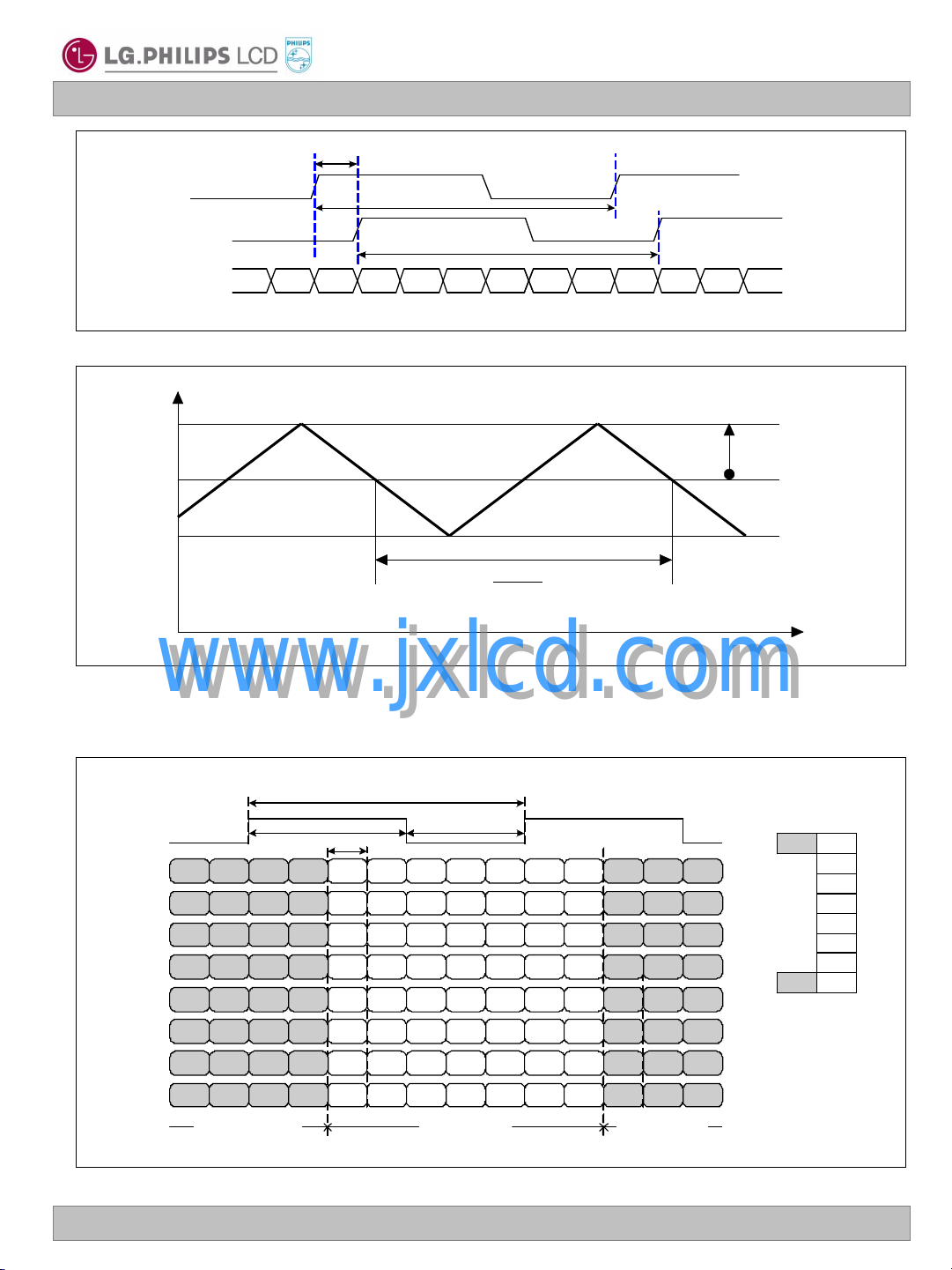
3-4. Signal Timing Specifications
This is the signal timing required at the input of the User connector. All of the interface signal timing should be
satisfied with the following specifications and specifications of LVDS Tx/Rx for its proper operation.
Table 6. TIMING TABLE
NoteUnitMaxTypMinSymbolITEM
FrequencyDCLK
Hsync
Vsync
Horizontal back porch
Data
Enable
3-5. Signal Timing Waveforms
Horizontal front porch
Vertical back porch
Vertical front porch
www.jxlcd.com
www.jxlcd.com
Data Enable, Hsync, Vsync
DCLK
tCLK
0.5 Vcc
f
CLK
ThpPeriod
tWH Width tCLK
t
Width-Active
WHA
tVP Period
tWV Width
t
Width-Active
WVA
t
HBP
t
HFP
t
VBP
t
VFP
High: 0.7VCC
Low: 0.3VCC
-75.375-
10401005990
401510
960960960
140012501207
631
120012001200
--10
--10
--5
--1
MHz
tHP
tCLK
tHP
Condition : VCC =3.3V
t
HP
Hsync
t
WH
t
HBP
tWHA
Data Enable
t
VP
t
WV
Vsync
t
VBP
tWVA
Data Enable
Ver. 1.2 Sep. 29, 2007
t
t
HFP
VFP
12 / 32
Page 13

LP154WU1
Liquid Crystal Display
Product Specification
3-6. Color Input Data Reference
The brightness of each primary color (red,green and blue) is based on the 6-bit gray scale data input for the
color ; the higher the binary input, the brighter the color. The table below provides a reference for color
versus data input.
Table 7. COLOR DATA REFERENCE
Input Color Data
Basic
Color
RED
GREEN
BLUE
Color
Black
Red
Green
Blue
Cyan
Magenta
Yellow
White
RED (00)
www.jxlcd.com
www.jxlcd.com
RED (01)
…
RED (62)
RED (63)
GREEN (00)
GREEN (01)
...
GREEN (62)
GREEN (63)
BLUE (00)
BLUE (01)
…
BLUE (62)
BLUE (63)
MSB LSB
RED
GREEN
MSB LSB
MSB LSB
B5 B4 B3 B2 B1 B0G5 G4 G3 G2 G1 G0R5 R4 R3 R2 R1 R0
BLUE
0 0 0 0 0 00 0 0 0 0 00 0 0 0 0 0
0 0 0 0 0 00 0 0 0 0 01 1 1 1 1 1
0 0 0 0 0 01 1 1 1 1 10 0 0 0 0 0
1 1 1 1 1 10 0 0 0 0 00 0 0 0 0 0
1 1 1 1 1 11 1 1 1 1 10 0 0 0 0 0
1 1 1 1 1 10 0 0 0 0 01 1 1 1 1 1
0 0 0 0 0 01 1 1 1 1 11 1 1 1 1 1
1 1 1 1 1 11 1 1 1 1 11 1 1 1 1 1
0 0 0 0 0 00 0 0 0 0 00 0 0 0 0 0
0 0 0 0 0 00 0 0 0 0 00 0 0 0 0 1
………
0 0 0 0 0 00 0 0 0 0 01 1 1 1 1 0
0 0 0 0 0 00 0 0 0 0 01 1 1 1 1 1
0 0 0 0 0 00 0 0 0 0 00 0 0 0 0 0
0 0 0 0 0 00 0 0 0 0 10 0 0 0 0 0
………
0 0 0 0 0 01 1 1 1 1 00 0 0 0 0 0
0 0 0 0 0 01 1 1 1 1 10 0 0 0 0 0
0 0 0 0 0 00 0 0 0 0 00 0 0 0 0 0
0 0 0 0 0 10 0 0 0 0 00 0 0 0 0 0
………
1 1 1 1 1 00 0 0 0 0 00 0 0 0 0 0
1 1 1 1 1 10 0 0 0 0 00 0 0 0 0 0
Ver. 1.2 Sep. 29, 2007
13 / 32
Page 14

3-7. Power Sequence
LP154WU1
Liquid Crystal Display
Product Specification
Power Supply For LCD
VCC
Interface Signal,
V
(LVDS Signal of Transmitter)
LAMP Power
i
www.jxlcd.com
www.jxlcd.com
90%
0V
T
0V
Table 8. POWER SEQUENCE TABLE
T
1
2
Valid Data
T
3
90%
10%10%
T
T
6
T
5
T
4
OFFOFF LAMP ON
UnitsValueParameter
7
Max.Typ.Min.
1
2
3
4
5
6
7
Note)
1. Valid Data is Data to meet “3-3. LVDS Signal Timing Specifications”
2. Please avoid floating state of interface signal at invalid period.
3. When the interface signal is invalid, be sure to pull down the power supply for LCD VCC to 0V.
4. Lamp power must be turn on after power supply for LCD and interface signal are valid.
Ver. 1.2 Sep. 29, 2007
(ms)10-0T
(ms)50-0T
(ms)--200T
(ms)--200T
(ms)50-0T
(ms)10-0T
(ms)--400T
14 / 32
Page 15

LP154WU1
Liquid Crystal Display
Product Specification
4. Optical Specification
Optical characteristics are determined after the unit has been ‘ON’ and stable for approximately 30 minutes in
a dark environment at 25C. The values specified are at an approximate distance 50cm from the LCD surface
at a viewing angle of and equal to 0.
FIG. 1 presents additional information concerning the measurement equipment and method.
FIG. 1 Optical Characteristic Measurement Equipment and Method
Optical Stage(x,y)
Parameter Symbol NotesUnits
www.jxlcd.com
www.jxlcd.com
Surface Luminance, white
Luminance Variation
Color Coordinates
RED
GREEN
BLUE
x axis, right(=0) 5
x axis, left (=180)
y axis, up (=90)
y axis, down (=270)
LCD Module
50cm
Table 9. OPTICAL CHARACTERISTICS
Ta=25C, VCC=3.3V, fV=60Hz, f
Values
WH
WHITE
R +TrD
CLK
MaxTypMin
0.6260.5960.566RX
0.3810.3510.321RY
0.3530.3230.293GX
0.5790.5490.519GY
0.1880.1580.128BX
0.1780.1480.118BYWHITE
0.3430.3130.283WX
0.3590.3290.299WYViewing Angle
Pritchard 880 or
equivalent
= 150.75MHz, F
-210180L
ms3016-Tr
degree--60r
degree--60l
degree--40u
degree--50dGray Scale
60KHz , IBL= 6.5mA
BL
=
2
±0.03
1--500CRContrast Ratio
2cd/m
22.0--
3Response Time
Ver. 1.2 Sep. 29, 2007
15 / 32
Page 16

LP154WU1
Liquid Crystal Display
Product Specification
Note)
1. Contrast Ratio(CR) is defined mathematically as
Surface Luminance with all white pixels
Contrast Ratio =
Surface Luminance with all black pixels
2. Surface luminance is the average of 5 point across the LCD surface 50cm from the surface with
all pixels displaying white. For more information see FIG 1.
LWH = Average(L1,L2, … L5)
3. The variation in surface luminance , The panel total variation (
at each test position 1 through 13 and then defined as followed numerical formula.
For more information see FIG 2.
Maximum(L1,L2, … L13)
Minimum(L1,L2, … L13)
4. Response time is the time required for the display to transition from white to black (rise time, TrR) and
from black to white(Decay Time, TrD). For additional information see FIG 3.
5. Viewing angle is the angle at which the contrast ratio is greater than 10. The angles are
for the horizontal or x axis and the vertical or y axis with respect to the z axis which is normal to the
LCD surface. For more information see FIG 4.
6. Gray scale specification * fV = 60Hz
=
WHITE
determined
www.jxlcd.com
www.jxlcd.com
Luminance [%] (Typ)Gray Level
L0
L7
L15
L23
L31
L39
L47
L55
L63
) is determined by measuring L
WHITE
0.1
1.0
4.0
11
21
35
53
75
100
N
Ver. 1.2 Sep. 29, 2007
16 / 32
Page 17

Product Specification
FIG. 2 Luminance
<measuring point for surface luminance & measuring point for luminance variation>
H
LP154WU1
Liquid Crystal Display
A
C
V
www.jxlcd.com
www.jxlcd.com
FIG. 3 Response Time
The response time is defined as the following figure and shall be measured by switching the input signal
for “black” and “white”.
L6
L2
B
L9
L4 L5
L11 L13
L7
L3
L1
Center Point
L12
D
L8
L10
H,V : ACTIVE AREA
A : H/4 mm
B : V/4 mm
C : 10 mm
D : 10 mm
POINTS : 13 POINTS
Tr
%
100
90
Optical
Response
10
0
white
Ver. 1.2 Sep. 29, 2007
R
black
Tr
D
white
17 / 32
Page 18

LP154WU1
Liquid Crystal Display
Product Specification
5. Mechanical Characteristics
The contents provide general mechanical characteristics for the model LP154WU1. In addition the figures
in the next page are detailed mechanical drawing of the LCD.
344.0 0.5mmHorizontal
Outline Dimension
Bezel Area
Active Display Area
575 g (Max.) without inverter & bracketWeight
Surface Treatment
www.jxlcd.com
www.jxlcd.com
Anti-glare treatment of the front polarizer
222.0 0.5mmVertical
6.2(typ) 0.3mmDepth
335.0 0.5mmHorizontal
210.7 0.5mmVertical
331.2 mmHorizontal
207.0 mmVertical
Ver. 1.2 Sep. 29, 2007
18 / 32
Page 19

Product Specification
LP154WU1
Liquid Crystal Display
<FRONT VIEW>
Note) Unit:[mm], General tolerance: 0.5mm
www.jxlcd.com
www.jxlcd.com
Ver. 1.2 Sep. 29, 2007
19 / 32
Page 20

Product Specification
LP154WU1
Liquid Crystal Display
<REAR VIEW>
Note) Unit:[mm], General tolerance: 0.5mm
www.jxlcd.com
www.jxlcd.com
Ver. 1.2 Sep. 29, 2007
20 / 32
Page 21

Product Specification
[ DETAIL DESCRIPTION OF SIDE MOUNTING SCREW ]
*Screw Torque (8 point):
LP154WU1
Liquid Crystal Display
www.jxlcd.com
www.jxlcd.com
Ver. 1.2 Sep. 29, 2007
Note) Unit:[mm], General tolerance: 0.5mm
21 / 32
Page 22

Product Specification
LPL Proposal for system cover design.(Appendix)
LP154WU1
Liquid Crystal Display
1
www.jxlcd.com
Gap check for securing the enough gap between LCM
and System cover.
1.Rear side of LCM is sensitive against external stress,and previous check
www.jxlcd.com
about interference is highly needed.
Define
Define
Ver. 1.2 Sep. 29, 2007
2.In case there is something from system cover comes into the boundary
above,mechanical interference may cause the FOS defects.
(Eg:Ripple,White spot..)
Check if antenna cable is sufficiently apart from T-CON of LCD Module. 2
NO GOOD
1.If system antenna is overlapped with T-CON,it might be cause the noise.
GOOD
22 / 32
Page 23

Product Specification
LPL Proposal for system cover design.
LP154WU1
Liquid Crystal Display
3
Define
Gap check for securing the enough gap between LCM
and System hinge.
1.At least 2.0mm of gap needs to be secured to prevent the shock
www.jxlcd.com
www.jxlcd.com
related defects.
2.”L” type of hinge is recommended than “I” type under shock test.
4
Define
Ver. 1.2 Sep. 29, 2007
Checking the path of the System wire.
#4#5#6
Good
1.COF area needs to be handled with care.
2.GOOD Wire path design to system side.
OK Wire path is located between COFs.
BADWire path overlapped with COF area.
Ok
Bad
#3
#2
#1
23 / 32
Page 24

Product Specification
LPL Proposal for system cover design.
5 Using a bracket on the top of LCM is not recommended.
bracket
LP154WU1
Liquid Crystal Display
Define
With bracket Without bracket
1.Condition without bracket is good for mechanical noise,and can minimize
the light leakage from deformation of bracket.
www.jxlcd.com
www.jxlcd.com
2.The results shows that there is no difference between the condition
with or without bracket.
Securing additional gap on CNT area..6
System cover inner side.
User connector
area.
User connector
Cable pathway.
A
A~A-1
A-1
cut
FPC:Flexible Printed Circuit.
1.CNT area is specially sensitive against external stress,and additional
Define
Ver. 1.2 Sep. 29, 2007
gap by cutting on system cover will be helpful on removing the Ripple.
2.Using a thinner CNT will be better. (eg: FPC type)
24 / 32
Page 25

6. Reliability
Environment test condition
LP154WU1
Liquid Crystal Display
Product Specification
ConditionsTest ItemNo.
High temperature storage test1
Low temperature storage test2
High temperature operation test3
Low temperature operation test4
Vibration test (non-operating)5
Shock test (non-operating)6
Altitude operating
7
storage / shipment
{ Result Evaluation Criteria }
There should be no change which might affect the practical display function when the display quality
test is conducted under normal operating condition.
www.jxlcd.com
www.jxlcd.com
Ta= 60C, 240h
Ta= -20C, 240h
Ta= 50C, 50%RH, 240h
Ta= 0C, 240h
Sine wave, 10 ~ 500 ~ 10Hz, 1.5G, 0.37oct/min
3 axis, 1hour/axis
Half sine wave, 180G, 2ms
one shock of each six faces(I.e. run 180G 6ms
for all six faces)
0 ~ 10,000 feet (3,048m) 24Hr
0 ~ 40,000 feet (12,192m) 24Hr
Ver. 1.2 Sep. 29, 2007
25 / 32
Page 26

Liquid Crystal Display
Product Specification
7. International Standards
7-1. Safety
a) UL 60950-1:2003, First Edition, Underwriters Laboratories, Inc.,
Standard for Safety of Information Technology Equipment.
b) CAN/CSA C22.2, No. 60950-1-03 1st Ed. April 1, 2003, Canadian Standards Association,
Standard for Safety of Information Technology Equipment.
c) EN 60950-1:2001, First Edition,
European Committee for Electrotechnical Standardization(CENELEC)
European Standard for Safety of Information Technology Equipment.
7-2. EMC
a) ANSI C63.4 “Methods of Measurement of Radio-Noise Emissions from Low-Voltage
Electrical and
Electrical Equipment in the Range of 9kHZ to 40GHz. “American National Standards
Institute(ANSI),
1992
b) C.I.S.P.R “Limits and Methods of Measurement of Radio Interface Characteristics of
Information
Technology Equipment.“ International Special Committee on Radio Interference.
Technology Equipment.“ European Committee for Electrotechnical
Standardization.(CENELEC), 1998
( Including A1: 2000 )
www.jxlcd.com
c) EN 55022 “Limits and Methods of Measurement of Radio Interface Characteristics of
www.jxlcd.com
Information
LP154WU1
Ver. 1.2 Sep. 29, 2007
26 / 32
Page 27

Product Specification
8. Packing
8-1. Designation of Lot Mark
a) Lot Mark
A B C D E F G H I J K L M
A,B,C : SIZE(INCH) D : YEAR
E : MONTH F ~ M : SERIAL NO.
Note
1. YEAR
LP154WU1
Liquid Crystal Display
Year
Mark
2. MONTH
Month
Mark
www.jxlcd.com
www.jxlcd.com
b) Location of Lot Mark
Serial No. is printed on the label. The label is attached to the backside of the LCD module.
This is subject to change without prior notice.
8-2. Packing Form
a) Package quantity in one box : 20 pcs
b) Box Size : 395mm ×390mm × 309mm
2006720078200892009
6
Jun7Jul8Aug9Sep
6
321
200452005
4
Apr5May
4
200320022001
2010
0
Oct
A
Nov
B
DecMarFebJan
C321
Ver. 1.2 Sep. 29, 2007
27 / 32
Page 28

LP154WU1
Liquid Crystal Display
Product Specification
9. PRECAUTIONS
Please pay attention to the followings when you use this TFT LCD module.
9-1. MOUNTING PRECAUTIONS
(1) You must mount a module using holes arranged in four corners or four sides.
(2) You should consider the mounting structure so that uneven force (ex. Twisted stress) is not applied to the
module. And the case on which a module is mounted should have sufficient strength so that
external
force is not transmitted directly to the module.
(3) Please attach the surface transparent protective plate to the surface in order to protect the polarizer.
Transparent protective plate should have sufficient strength in order to the resist external force.
(4) You should adopt radiation structure to satisfy the temperature specification.
(5) Acetic acid type and chlorine type materials for the cover case are not desirable because the former
generates corrosive gas of attacking the polarizer at high temperature and the latter causes
circuit break
by electro-chemical reaction.
(6) Do not touch, push or rub the exposed polarizers with glass, tweezers or anything harder than HB
pencil lead. And please do not rub with dust clothes with chemical treatment.
Do not touch the surface of polarizer for bare hand or greasy cloth.(Some cosmetics are detrimental
to the polarizer.)
(7) When the surface becomes dusty, please wipe gently with absorbent cotton or other soft materials like
chamois soaks with petroleum benzene. Normal-hexane is recommended for cleaning the
www.jxlcd.com
www.jxlcd.com
used to attach front / rear polarizers. Do not use acetone, toluene and alcohol because they
chemical damage to the polarizer.
(8) Wipe off saliva or water drops as soon as possible. Their long time contact with polarizer causes
deformations and color fading.
9-2. OPERATING PRECAUTIONS
(9) Do not open the case because inside circuits do not have sufficient strength.
adhesives
cause
(1) The spike noise causes the mis-operation of circuits. It should be lower than following voltage :
V=± 200mV(Over and under shoot voltage)
(2) Response time depends on the temperature.(In lower temperature, it becomes longer.)
(3) Brightness depends on the temperature. (In lower temperature, it becomes lower.)
And in lower temperature, response time(required time that brightness is stable after turned on) becomes
longer.
(4) Be careful for condensation at sudden temperature change. Condensation makes damage to polarizer or
electrical contacted parts. And after fading condensation, smear or spot will occur.
(5) When fixed patterns are displayed for a long time, remnant image is likely to occur.
(6) Module has high frequency circuits. Sufficient suppression to the electromagnetic interference shall be
done by system manufacturers. Grounding and shielding methods may be important to minimized the
interference.
Ver. 1.2 Sep. 29, 2007
28 / 32
Page 29

LP154WU1
Liquid Crystal Display
Product Specification
9-3. ELECTROSTATIC DISCHARGE CONTROL
Since a module is composed of electronic circuits, it is not strong to electrostatic discharge. Make certain that
treatment persons are connected to ground through wrist band etc. And don’t touch interface pin directly.
9-4. PRECAUTIONS FOR STRONG LIGHT EXPOSURE
Strong light exposure causes degradation of polarizer and color filter.
9-5. STORAGE
When storing modules as spares for a long time, the following precautions are necessary.
(1) Store them in a dark place. Do not expose the module to sunlight or fluorescent light. Keep the
temperature between 5C and 35C at normal humidity.
(2) The polarizer surface should not come in contact with any other object.
It is recommended that they be stored in the container in which they were shipped.
9-6. HANDLING PRECAUTIONS FOR PROTECTION FILM
(1) When the protection film is peeled off, static electricity is generated between the film and polarizer.
This should be peeled off slowly and carefully by people who are electrically grounded and with well
ion-blown equipment or in such a condition, etc.
(2) The protection film is attached to the polarizer with a small amount of glue. If some stress is applied
to rub the protection film against the polarizer during the time you peel off the film, the glue is apt to
remain on the polarizer.
Please carefully peel off the protection film without rubbing it against the polarizer.
(3) When the module with protection film attached is stored for a long time, sometimes there remains a
very small amount of glue still on the polarizer after the protection film is peeled off.
(4) You can remove the glue easily. When the glue remains on the polarizer surface or its vestige is
recognized, please wipe them off with absorbent cotton waste or other soft material like chamois
soaked with normal-hexane.
www.jxlcd.com
www.jxlcd.com
Ver. 1.2 Sep. 29, 2007
29 / 32
Page 30

Liquid Crystal Display
Byte Value Value
(hex) (hex) (binary)
0 Header
00
00000000
1 Header
FF
11111111
2 Header
FF
11111111
3 Header
FF
11111111
4 Header
FF
11111111
5 Header
FF
11111111
6 Header
FF
11111111
7 Header
00
00000000
8 EISA manufacture code = 3 Character ID=LPL
32
00110010
9 EISA manufacture code (Compressed ASCII)
0C
00001100
0A Panel Supplier Reserved – Product Code
00
00000000
0B Panel Supplier Reserved – Product Code
F2
11110010
0C LCD module Serial No - Preferred but Optional (“0” if not used)
00
00000000
0D LCD module Serial No - Preferred but Optional (“0” if not used)
00
00000000
0E LCD module Serial No - Preferred but Optional (“0” if not used)
00
00000000
0F LCD module Serial No - Preferred but Optional (“0” if not used)
00
00000000
10 Week of manufacture
00
00000000
11 Year of manufacture =2007
11
00010001
12 EDID structure version # = 1
01
00000001
13 EDID revision # = 3
03
00000011
14 Video I/P definition = Digital I/P (80h)
80
10000000
15 Max H image size =33.138cm (Rounded to cm) (33)
21
00100001
16 Max V image size =20.711 (Rounded to cm) (21)
15
00010101
17 Display gamma = (gamma ×100)-100 = Example: ( 2.2×100 ) – 100 = 120
78
01111000
18 Feature support ( no DPMS, Active off, RGB, timing BLK 1)
EA
11101010
19 Red/Green Low bit (RxRy/GxGy)
BA
10111010
1A Blue/White Low bit (BxBy/WxWy)
70
01110000
1B Red X Rx = 0.596
98
10011000
1C Red Y Ry = 0.351
59
01011001
1D Green X Gx = 0.323
52
01010010
1E Green Y Gy = 0.549
8C
10001100
1F Blue X Bx = 0.158
28
00101000
20 Blue Y By = 0.148
25
00100101
21 White X Wx = 0.313
50
01010000
22 White Y Wy = 0.329
54
01010100
23 Established timings 1 (00h if not used)
21
00100001
24 Established timings 2 (00h if not used)
08
00001000
25 Manufacturer’s timings (00h if not used)
00
00000000
26 Standard timing ID1 (01h if not used)
81
10000001
27 Standard timing ID1 (01h if not used)
80
10000000
28 Standard timing ID2 (01h if not used)
A9
10101001
29 Standard timing ID2 (01h if not used)
40
01000000
2A Standard timing ID3 (01h if not used)
01
00000001
2B Standard timing ID3 (01h if not used)
01
00000001
2C Standard timing ID4 (01h if not used)
01
00000001
2D Standard timing ID4 (01h if not used)
01
00000001
2E Standard timing ID5 (01h if not used)
01
00000001
2F Standard timing ID5 (01h if not used)
01
00000001
30 Standard timing ID6 (01h if not used)
01
00000001
31 Standard timing ID6 (01h if not used)
01
00000001
32 Standard timing ID7 (01h if not used)
01
00000001
33 Standard timing ID7 (01h if not used)
01
00000001
34 Standard timing ID8 (01h if not used)
01
00000001
35 Standard timing ID8 (01h if not used)
01
00000001
Panel Color
Coordinates
Standard Timing ID
Established
Timings
Field Name and Comments
Vendor / Product
EDID Version
Display
Parameters
Header
Product Specification
APPENDIX A. Enhanced Extended Display Identification Data (EEDIDTM) 1/3
LP154WU1
www.jxlcd.com
www.jxlcd.com
Ver. 1.2 Sep. 29, 2007
30 / 32
Page 31

Liquid Crystal Display
Byte Value Value
(hex) (hex) (binary)
36 Pixel Clock/10,000 150.75MHz (LSB)
E3
11100011
37 Pixel Clock/10,000 150.75MHz (MSB)
3A
00111010
38 Horizontal Active = 1920 pixels (lower 8 bits)
80
10000000
39 Horizontal Blanking (Thbp) = 90 pixels (lower 8 bits)
5A
01011010
3A Horizontal Active/Horizontal blanking (Thbp) (upper4:4 bits)
70
01110000
3B Vertical Active = 1200lines
B0
10110000
3C Vertical Blanking (Tvbp) = 50 lines (DE Blanking typ. for DE only panels)
32
00110010
3D Vertical Active : Vertical Blanking (Tvbp) (upper4:4 bits)
40
01000000
3E Horizontal Sync, Offset (Thfp) = 30 pixels
1E
00011110
3F Horizontal Sync, Pulse Width = 30 pixels
1E
00011110
40 Vertical Sync, Offset (Tvfp) = 1 lines Sync Width =3 lines
13
00010011
41 Horizontal Vertical Sync Offset/Width upper 2 bits
00
00000000
42 Horizontal Image Size =331.38 mm(331)
4B
01001011
43 Vertical image Size = 207.11 mm(207)
CF
11001111
44 Horizontal Image Size / Vertical image size
10
00010000
45 Horizontal Border = 0 (Zero for Notebook LCD)
00
00000000
46 Vertical Border = 0 (Zero for Notebook LCD)
00
00000000
47
Non-interlaced, Normal, no stereo, Separate sync, H/V pol Negatives,
DE only note: LSB is set to “1” if
panel is DE-timing only. H/V can be ignored.
19
00011001
48 Pixel Clock/10,000 150.75MHz (LSB)
00
00000000
49 Pixel Clock/10,000 150.75MHz (MSB)
00
00000000
4A Horizontal Active = 1920 pixels (lower 8 bits)
00
00000000
4B Horizontal Blanking (Thbp) = 90 pixels (lower 8 bits)
00
00000000
4C Horizontal Active/Horizontal blanking (Thbp) (upper4:4 bits)
00
00000000
4D Vertical Active = 1200lines
00
00000000
4E Vertical Blanking (Tvbp) = 50 lines (DE Blanking typ. for DE only panels)
00
00000000
4F Vertical Active : Vertical Blanking (Tvbp) (upper4:4 bits)
00
00000000
50 Horizontal Sync, Offset (Thfp) = 30 pixels
00
00000000
51 Horizontal Sync, Pulse Width = 30 pixels
00
00000000
52 Vertical Sync, Offset (Tvfp) = 1 lines Sync Width =3 lines
00
00000000
53 Horizontal Vertical Sync Offset/Width upper 2 bits
00
00000000
54 Horizontal Image Size =331.38 mm(331)
00
00000000
55 Vertical image Size = 207.11 mm(207)
00
00000000
56 Horizontal Image Size / Vertical image size
00
00000000
57 Horizontal Border = 0 (Zero for Notebook LCD)
00
00000000
58 Vertical Border = 0 (Zero for Notebook LCD)
00
00000000
59 Module “A” Revision = Example: 00, 01, 02, 03, etc.
00
00000000
5A Flag
00
00000000
5B Flag
00
00000000
5C Flag
00
00000000
5D Dummy Descriptor
FE
11111110
5E Flag
00
00000000
5F Dell P/N 1st Character =X
58
01011000
60 Dell P/N 2nd Character=U
55
01010101
61 Dell P/N 3rd Character=3
33
00110011
62 Dell P/N 4th Character=0
30
00110000
63 Dell P/N 5th Character=1
31
00110001
64 LCD Supplier EEDID Revision # =VER 0.4
04
00000100
65 Manufacturer P/N=1
31
00110001
66 Manufacturer P/N=5
35
00110101
67 Manufacturer P/N=4
34
00110100
68 Manufacturer P/N=W
57
01010111
69 Manufacturer P/N=U
55
01010101
6A Manufacturer P/N=1
31
00110001
6B Manufacturer P/N (If <13 char, then terminate with ASCII code 0Ah, set remaining char = 20h)
0A
00001010
Timing Descripter #1
Timing Descripter #2
Timing Descripter #3
Dell specific information
Field Name and Comments
Product Specification
APPENDIX A. Enhanced Extended Display Identification Data (EEDIDTM) 2/3
LP154WU1
www.jxlcd.com
www.jxlcd.com
Ver. 1.2 Sep. 29, 2007
31 / 32
Page 32

Liquid Crystal Display
Byte Value Value
(hex) (hex) (binary)
6C Flag
00
00000000
6D Flag
00
00000000
6E Flag
00
00000000
6F Data Type Tag:
FE
11111110
70 Flag
00
00000000
71
SMBUS Value = 10 nits +/- 10% (5 - point average)
28
00101000
72
SMBUS Value = 17 nits +/- 10% (5 - point average)
3E
00111110
73
SMBUS Value = 24 nits +/- 10% (5 - point average)
4C
01001100
74
SMBUS Value = 30 nits +/- 10% (5 - point average)
53
01010011
75
SMBUS Value = 60 nits +/- 10% (5 - point average)
73
01110011
76
SMBUS Value = 110 nits +/- 10% (5 - point average)
9B
10011011
77
SMBUS Value = 150 nits +/- 10% (5 - point average)
BA
10111010
78
SMBUS Value = MAX nits (Typically = FFh, XXX nits)
FF
11111111
79 Number of LVDS receiver chips = ‘01’ or ‘02’
02
00000010
7A BIST Enable: Yes = ‘01’ No = ‘00’
01
00000001
7B (If <13 char, then terminate with ASCII code 0Ah, set remaining char = 20h)
0A
00001010
7C (If <13 char, then terminate with ASCII code 0Ah, set remaining char = 20h)
20
00100000
7D (If <13 char, then terminate with ASCII code 0Ah, set remaining char = 20h)
20
00100000
7E Extension flag (# of optional 128 EDID extension blocks to follow, Typ = 0)
00
00000000
7F Checksum (The 1-byte sum of all 128 bytes in this EDID block shall = 0) AA 10101010
Checksum
Timing Descripter #4
Field Name and Comments
Product Specification
APPENDIX A. Enhanced Extended Display Identification Data (EEDIDTM) 3/3
LP154WU1
www.jxlcd.com
www.jxlcd.com
Ver. 1.2 Sep. 29, 2007
32 / 32
 Loading...