

Page 1
Product Specification
SPECIFICATION
LP150X09
Liquid Crystal Display
FOR
APPROVAL
)
(
(
Preliminary Specification
)
Final Specification
◆
MODEL
www.jxlcd.com
www.jxlcd.com
15.0” XGA TFT LCDTitle
GeneralBUYER
*When you obtain standard approval,
please use the above model name without suffix
LG.Philips LCD Co., Ltd.SUPPLIER
LP150X09*MODEL
B5K8Suffix
SIGNATUREAPPROVED BY
/
/
/
Please return 1 copy for your confirmation with
your signature and comments.
Ver. 1.1 Oct. 23. 2007
SIGNATUREAPPROVED BY
S. C. Yoon / S.Manager
REVIEWED BY
G.J. Han / Manager
J.W. Park / Manager
PREPARED BY
I. Y. Jung / Engineer
J.H. Kim / Engineer
Products Engineering Dept.
LG. Philips LCD Co., Ltd
1 / 27
Page 2
Product Specification
Contents
LP150X09
Liquid Crystal Display
ITEMNo
COVER
CONTENTS
RECORD OF REVISIONS
GENERAL DESCRIPTION1
ABSOLUTE MAXIMUM RATINGS2
ELECTRICAL SPECIFICATIONS3
ELECTRICAL CHARACTERISTICS 3-1
INTERFACE CONNECTIONS 3-2
SIGNAL TIMING SPECIFICATIONS 3-3
SIGNAL TIMING WAVEFORMS 3-4
COLOR INPUT DATA REFERNECE 3-5
www.jxlcd.com
www.jxlcd.com
POWER SEQUENCE 3-6
OPTICAL SFECIFICATIONS4
MECHANICAL CHARACTERISTICS5
Page
1
2
3
4
5
6
7
9
9
10
11
12
16
RELIABILITY6
INTERNATIONAL STANDARDS7
SAFETY 7-1
EMC 7-2
PACKING8
DESIGNATION OF LOT MARK 8-1
PACKING FORM 8-2
PRECAUTIONS9
APPENDIX. Enhanced Extended Display Identification Data A
Ver. 1.1 Oct. 23. 2007
20
21
21
22
22
23
25
2 / 27
Page 3
Product Specification
RECORD OF REVISIONS
LP150X09
Liquid Crystal Display
DescriptionPageRevision DateRevision No
-12. 10. 20051.0
Final Specifications
4
Power consumption changed
Electrical characteristics changed6
10. 23. 20071.1
www.jxlcd.com
www.jxlcd.com
LCD Interface chip changed7
Timing table updated9
color coordinates changed12
EDID
Ver.
1.0
1.0
Ver. 1.1 Oct. 23. 2007
3 / 27
Page 4
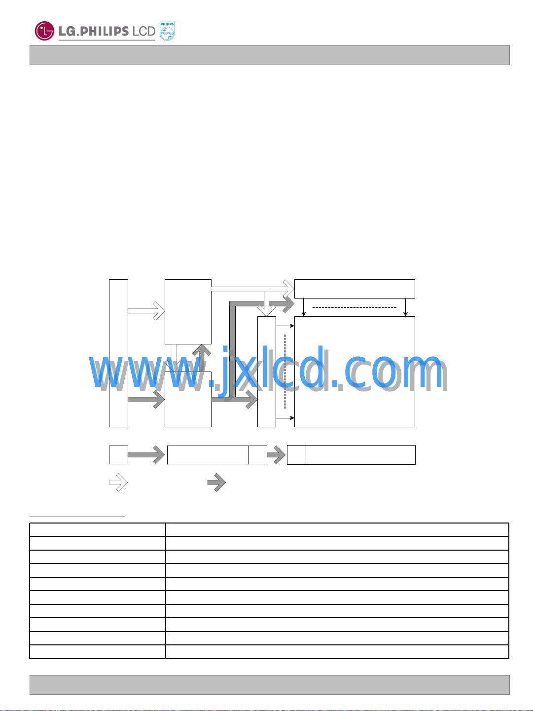
LP150X09
CN1
LVDS
&
Timing
Control
Block
Power
Block
Column Driver Circuit
Row Dirver Circuit
TFT-LCD
(1024 X 768)
J1
:Control & Data :Power
B/L Inverter
J2
Backlight Ass'y
J3
Liquid Crystal Display
Product Specification
1. General Description
The LP150X09 is a Color Active Matrix Liquid Crystal Display with an integral Cold Cathode Fluorescent
Lamp (CCFL) backlight system. The matrix employs a-Si Thin Film Transistor as the active element. It is a
transmissive type display operating in the normally white mode. This TFT-LCD has 15.0 inches diagonally
measured active display area with XGA resolution(768 vertical by 1024 horizontal pixel array). Each pixel is
divided into Red, Green and Blue sub-pixels or dots which are arranged in vertical stripes. Gray scale or the
brightness of the sub-pixel color is determined with a 6-bit gray scale signal for each dot, thus, presenting a
palette of more than 262,144 colors.
The LP150X09 has been designed to apply the interface method that enables low power, high speed, low
EMI.
The LP150X09 is intended to support applications where thin thickness, low power are critical factors and
graphic displays are important. In combination with the vertical arrangement of the sub-pixels, the LP150X09
characteristics provide an excellent flat display for office automation products such as Notebook PC.
General Features
www.jxlcd.com
www.jxlcd.com
15.0 inches(38.1cm) diagonal Active Screen Size
317.3(H) × 241.5(V) × 5.7(D) mm (Typ.)Outline Dimension
0.297 mm × 0.297 mm Pixel Pitch
1024 horiz. By 768 vert. Pixels RGB strip arrangementPixel Format
6-bit, 262,144 colorsColor Depth
180 cd/m2(Typ.), 5p averageLuminance, White
Total 4.96 Watt (Typ.)Power Consumption
575 g(Max.) with inverter and bracketWeight
Transmissive mode, normally whiteDisplay Operating Mode
Hard coating(3H) Anti-glare treatment of the front polarizerSurface Treatment
Ver. 1.1 Oct. 23. 2007
4 / 27
Page 5
LP150X09
Liquid Crystal Display
Product Specification
2. Absolute Maximum Ratings
The following are maximum values which, if exceeded, may cause faulty operation or damage to the unit.
Table 1. ABSOLUTE MAXIMUM RATINGS
Parameter Notes
Power Input Voltage
Operating Temperature
Storage Temperature
Operating Ambient Humidity
Storage Humidity
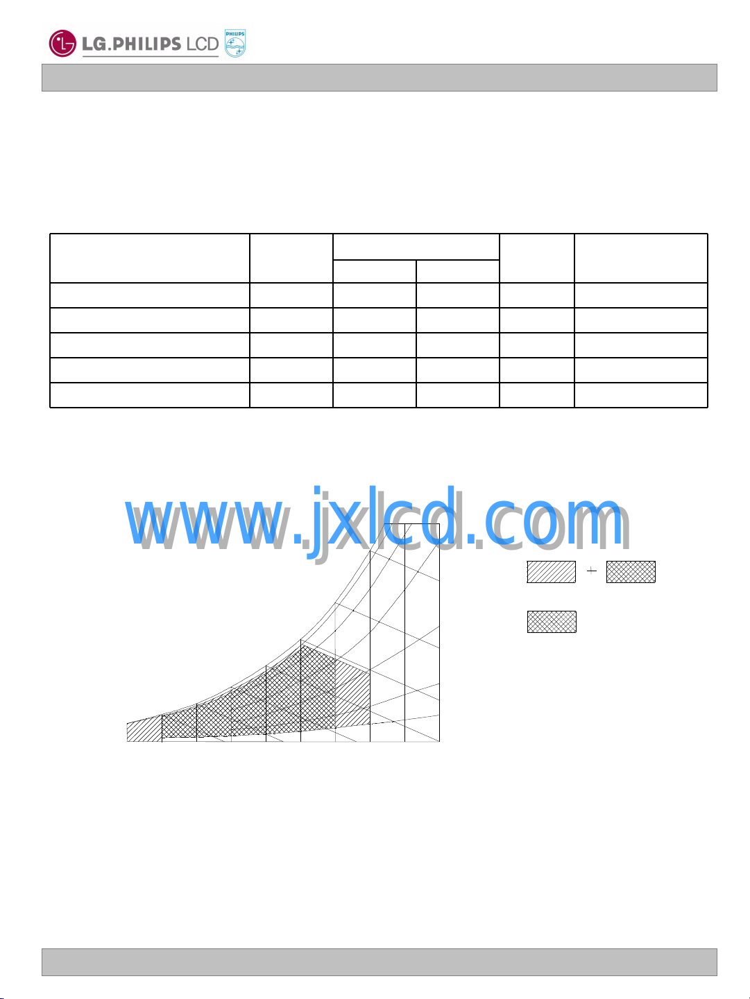
Note : 1. Temperature and relative humidity range are shown in the figure below.
Wet bulb temperature should be 39C Max, and no condensation of water.
www.jxlcd.com
www.jxlcd.com
Wet Bulb
Temperature [℃]
20
10
0
Symbol
60
50
40
30
Values
MaxMin
90% 80%
60%
40%
20%
10%
Units
Humidity[(%)RH]
Storage
Operation
at 25 5CVdc4.0-0.3VCC
1C500TOP
1C60-20HST
1%RH9010HOP
1%RH9010HST
-20
Ver. 1.1 Oct. 23. 2007
10
20 30 40 50
Dry Bulb Temperature [℃]
60 70 800
5 / 27
Page 6
LP150X09
Liquid Crystal Display
Product Specification
3. Electrical Specifications
3-1. Electrical Characteristics
The LP150X09 requires two power inputs. One is employed to power the LCD electronics and to drive the
TFT array and liquid crystal. The second input which powers the CCFL, is typically generated by an
inverter. The inverter is an external unit to the LCD.
Table 2. ELECTRICAL CHARACTERISTICS
Parameter Symbol
MODULE :
Power Supply Input Current
Differential Impedance
LAMP :
Operating Voltage
Operating Current
Operating Frequency
INVERTER :
Input Voltage
Input Current
Input Power Consumption
Output Voltage
Output Power Consumption
Open Lamp Voltage
Striking Time
www.jxlcd.com
www.jxlcd.com
OUT
OUT
CC
Zm
BL
BL
BL
IN
IN
IN
OUT
_FF Output Current (Aging 30minutes)
_00
OUT
OPEN
S
Values
DC
RMS
RMS
DC
DC
DC
RMS
RMS
RMS
RMS
NotesUnit
1mA260230-I
1Watt0.860.76-Pc Power Consumption
2Ohm11010090
3mA
4Min3--Ts Discharge Stabilization Time
5Hrs--15,000 Life Time
6mA-360-I
6W-5.18-P
7V
7mA
7KHz65-45Freq. Operating Frequency
6W4.914.283.65P
8V
9%--75 Efficiency
8sec1.4-0.6T
MaxTypMin
3.63.33.0VCC Power Supply Input Voltage
870(2.0mA)665(6.3mA)630(7.0mA)V
7.06.32.0I
21.014.47.5V
5.25-2.0FPVEE_High Backlight On/Off Control
0.8--0.3FPVEE_Low
780680580V
--2I
6.66.36.0I
1800-1400V
V
V
kHz806550f
V
V
V
Hex00-FF Backlight Adjust (IBL Control)
mA
Note)
1. The specified current and power consumption are under the Vcc = 3.3V , 25℃, fv = 60Hz condition
whereas Mosaic Pattern is displayed and fv is the frame frequency.
2. This impedance value is needed to proper display and measured form LVDS Tx to the mating connector.
3. The typical operating current is for the typical surface luminance (LWH) in optical characteristics.
Ver. 1.1 Oct. 23. 2007
6 / 27
Page 7
LP150X09
Liquid Crystal Display
Product Specification
Note)
4. Define the brightness of the lamp after being lighted for 5 minutes as 100%, Ts is the time required for
the brightness of the center of the lamp to be not less than 95%.
5. The life time is determined as the time at which brightness of lamp is 50% compare to that of initial value
at the typical lamp current.
6. VIN = 14.4V(Typ.), 28_H
7. SMData=00_H
8. No Load, SMData=00_H.
9. VIN =7.5V(Min.), 00H.
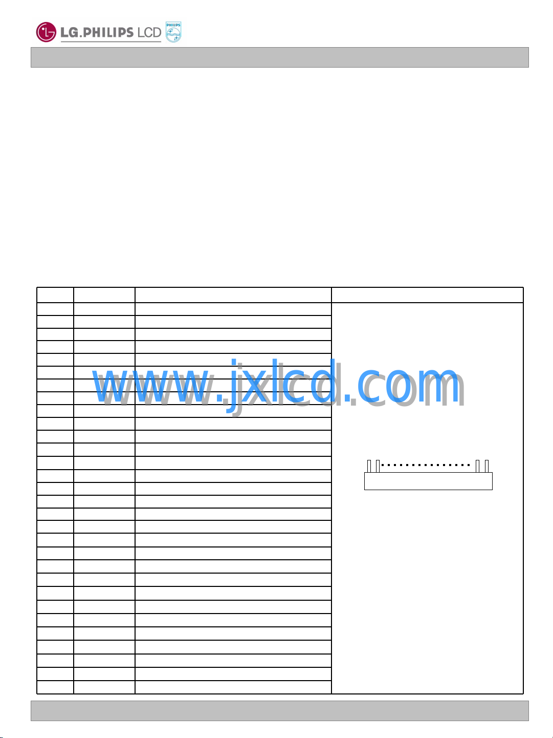
3-2. Interface Connections
This LCD employs two interface connections, a 30 pin connector is used for the module electronics interface
and the other connector is used for the integral backlight system.
The electronics interface connector is a model FI-XB30SRL-HF11 manufactured by JAE.
Table 3. MODULE CONNECTOR PIN CONFIGURATION (CN1)
NotesDescriptionSymbolPin
GroundGND1
Power Supply, 3.3V Typ.VCC2
Power Supply, 3.3V Typ.VCC3
1, Interface chips
1.1 LCD : SiW, SiWLVDSRx
1.2 System : it must include international
standard LVDS Transmitter.
* Pin to Pin compatible with LVDS
2. Connector
2.1 LCD : FI-XB30SRL-HF11, JAE or
MDF76LBRW-30S-1H, HIROSE
2.2 Mating : FI-X30M or equivalent.
2.3 Connector pin arrangement
30
[LCD Module Rear View]
1
10
11
12
13
14
15
16
17
18
19
20
21
22
23
24
25
26
27
28
29
30
4
5
6
7
8
9
www.jxlcd.com
www.jxlcd.com
RIN 1- Negative LVDS differential data input
NC
GND
DDC 3.3V powerV EEDID
Reserved for supplier Bist test pointBIST
DDC ClockClk EEDID
DDC DataDATA EEDID
Negative LVDS differential data inputRIN 0-
Positive LVDS differential data inputRIN 0+
GroundGND
Positive LVDS differential data inputRIN 1+
GroundGND
Negative LVDS differential data inputRIN 2-
Positive LVDS differential data inputRIN 2+
GroundGND
Negative LVDS differential clock inputCLKIN-
Positive LVDS differential clock inputCLKIN+
GroundGND
No connectionNC
No connection
Ground
No connectionNC
No connectionNC
GroundGND
No connectionNC
No connectionNC
GroundGND
No connectionNC
No connectionNC
Ver. 1.1 Oct. 23. 2007
7 / 27
Page 8
LP150X09
Liquid Crystal Display
Product Specification
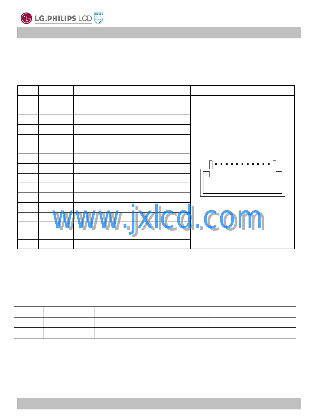
The inverter interface connector(J1) is a LVC-D20SFYG model manufactured by Honda. The pin configuration
for the connector is shown in the table below.
Table 4. BACKLIGHT INVERTER CONNECTOR PIN CONFIGURATION (J1)
NotesDescriptionSymbolPin
2
3
14
V
IN
IN
IN
www.jxlcd.com
www.jxlcd.com
LAMP_STAT
Power for the inverter 1
Power for the inverter V
Power for the inverter V
No connectionNC4
GroundGND5
Power for the control circuit5V_SUS6
Power for storing a brightness values5V_ALW7
GroundGND8
Brightness dataSMB_DAT9
Clock for brightness dataSMB_CLK10
GroundGND11
Enable for lamp turn on and offFPVEE12
GroundGND13
Lamp status (Feedback, Lamp On = 5V,
Lamp Off 0V), from control chip
No ConnectionNC15~20
[Connector]
LVC-D20SFYG, Honda
[Connector pin arrangement]
1 20
The backlight interface connector is a model BHSR-02VS-1, manufactured by JST or a model 1376176-1,
manufactured by AMP. The mating connector part number is SM02B-BHSS-1 or equivalent.
Table 5. BACKLIGHT CONNECTOR PIN CONFIGURATION (J3)
NotesDescriptionSymbolPin
1Power supply for lamp (High voltage side)HV1
1Power supply for lamp (Low voltage side)LV2
Notes : 1. The high voltage side terminal is colored pink and the low voltage side terminal is white
Ver. 1.1 Oct. 23. 2007
8 / 27
Page 9
LP150X09
Liquid Crystal Display
Product Specification
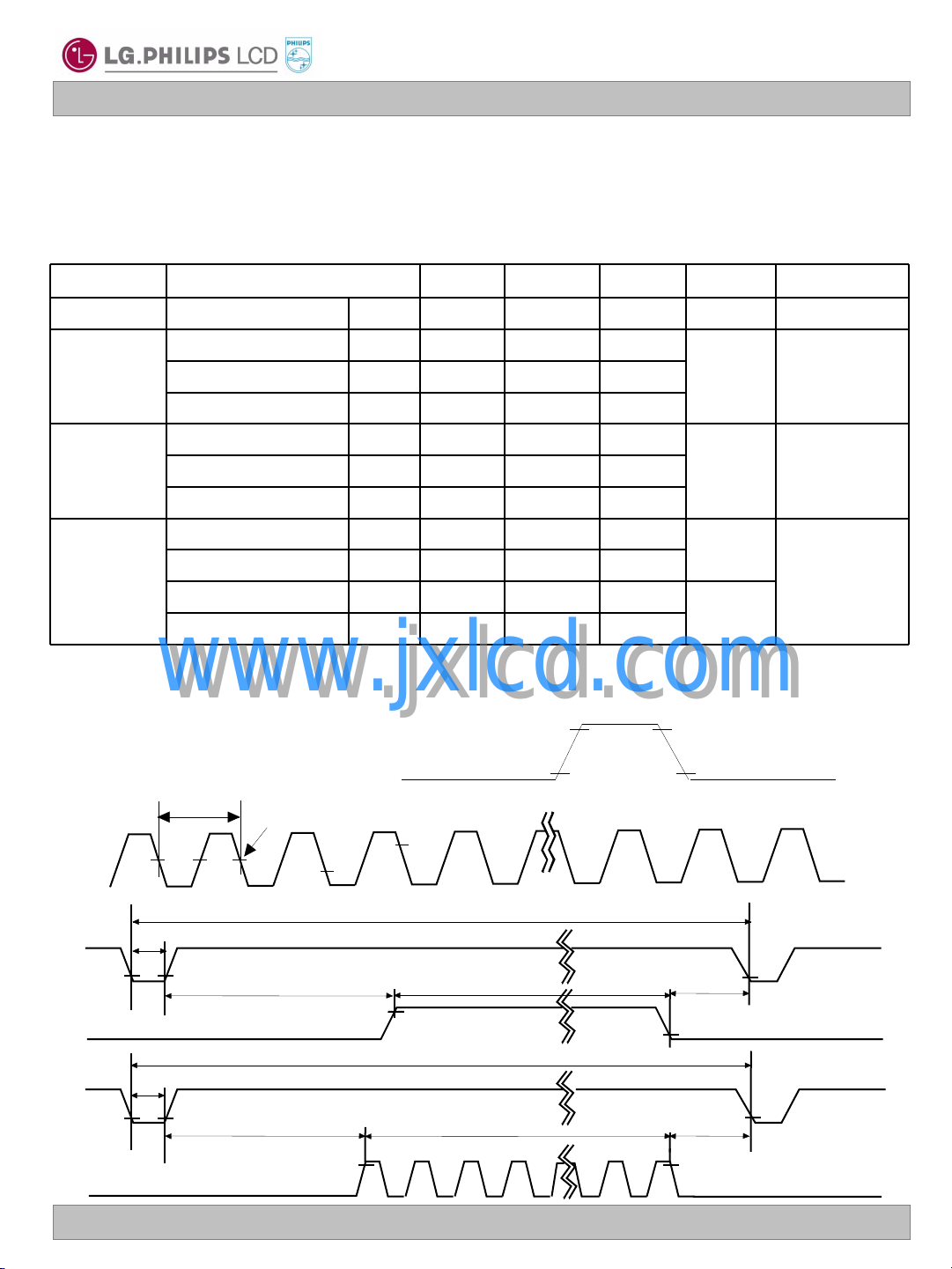
3-3. Signal Timing Specifications
This is the signal timing required at the input of the User connector. All of the interface signal timing should be
satisfied with the following specifications and specifications of LVDS Tx/Rx for it’s proper operation.
Table 6. TIMING TABLE
NoteUnitMaxTypMinSymbolITEM
Vsync
Data
Enable
3-4. Signal Timing Waveforms
www.jxlcd.com
www.jxlcd.com
Data Enable, Hsync, Vsync
DCLK
tCLK
0.5 Vcc
fCLK FrequencyDCLK
tHPPeriodHsync
tWH Width
tWHA Width-Active
tVP Period
tWV Width
tWVA Width-Active
tHBPHorizontal back porch
tHFPHorizontal front porch
tVBPVertical back porch
tVFPVertical front porch
High: 0.7VCC
Low: 0.3VCC
136413441206
3081368
102410241024
830806780
5461
768768768
31616010
3162410
60297
5431
tCLK
tHP
tCLK
tHP
Condition : VCC =3.3V
15.4nsMHz686562
t
HP
Hsync
Data Enable
Vsync
Ver. 1.1 Oct. 23. 2007
t
WH
t
WV
Data Enable
t
VBP
t
HBP
tWHA
t
VP
tWVA
t
t
HFP
VFP
9 / 27
Page 10

LP150X09
Liquid Crystal Display
Product Specification
3-5. Color Input Data Reference
The brightness of each primary color (red,green and blue) is based on the 6-bit gray scale data input for the
color ; the higher the binary input, the brighter the color. The table below provides a reference for color
versus data input.
Table 7. COLOR DATA REFERENCE
Input Color Data
Basic
Color
RED
GREEN
BLUE
Color
Black
Red
Green
Blue
Cyan
Magenta
Yellow
White
RED (00)
www.jxlcd.com
www.jxlcd.com
RED (01)
…
RED (62)
RED (63)
GREEN (00)
GREEN (01)
...
GREEN (62)
GREEN (63)
BLUE (00)
BLUE (01)
…
BLUE (62)
BLUE (63)
MSB LSB
RED
GREEN
MSB LSB
MSB LSB
B5 B4 B3 B2 B1 B0G5 G4 G3 G2 G1 G0R5 R4 R3 R2 R1 R0
BLUE
0 0 0 0 0 00 0 0 0 0 00 0 0 0 0 0
0 0 0 0 0 00 0 0 0 0 01 1 1 1 1 1
0 0 0 0 0 01 1 1 1 1 10 0 0 0 0 0
1 1 1 1 1 10 0 0 0 0 00 0 0 0 0 0
1 1 1 1 1 11 1 1 1 1 10 0 0 0 0 0
1 1 1 1 1 10 0 0 0 0 01 1 1 1 1 1
0 0 0 0 0 01 1 1 1 1 11 1 1 1 1 1
1 1 1 1 1 11 1 1 1 1 11 1 1 1 1 1
0 0 0 0 0 00 0 0 0 0 00 0 0 0 0 0
0 0 0 0 0 00 0 0 0 0 00 0 0 0 0 1
………
0 0 0 0 0 00 0 0 0 0 01 1 1 1 1 0
0 0 0 0 0 00 0 0 0 0 01 1 1 1 1 1
0 0 0 0 0 00 0 0 0 0 00 0 0 0 0 0
0 0 0 0 0 00 0 0 0 0 10 0 0 0 0 0
………
0 0 0 0 0 01 1 1 1 1 00 0 0 0 0 0
0 0 0 0 0 01 1 1 1 1 10 0 0 0 0 0
0 0 0 0 0 00 0 0 0 0 00 0 0 0 0 0
0 0 0 0 0 10 0 0 0 0 00 0 0 0 0 0
………
1 1 1 1 1 00 0 0 0 0 00 0 0 0 0 0
1 1 1 1 1 10 0 0 0 0 00 0 0 0 0 0
Ver. 1.1 Oct. 23. 2007
10 / 27
Page 11

3-6. Power Sequence
LP150X09
Liquid Crystal Display
Product Specification
Power Supply For LCD
VCC
Interface Signal,
V
(LVDS Signal of Transmitter)
FPVEE
Power for Inverter
V
i
www.jxlcd.com
IN
www.jxlcd.com
0V
90%
T
T
1
2
Valid Data
0V
T
3
T
8
8.5V
Table 8. POWER SEQUENCE TABLE
90%
10%10%
T
T
6
T
5
T
4
OFFOFF LAMP ON
7
UnitsValueParameter
Max.Typ.Min.
1
2
3
4
5
6
7
8
Note)
1. Please avoid floating state of interface signal at invalid period.
2. When the interface signal is invalid, be sure to pull down the power supply for LCD VCC to 0V.
3. Lamp power must be turn on after power supply for LCD and interface signal are valid.
Ver. 1.1 Oct. 23. 2007
(ms)10--T
(ms)50-0T
(ms)--200T
(ms)--0T
(ms)50-0T
(ms)10-0T
(ms)--400T
(ms)--10T
11 / 27
Page 12

LP150X09
Liquid Crystal Display
Product Specification
4. Optical Specification
Optical characteristics are determined after the unit has been ‘ON’ and stable for approximately 30 minutes in
a dark environment at 25C. The values specified are at an approximate distance 50cm from the LCD surface
at a viewing angle of and equal to 0.
FIG. 1 presents additional information concerning the measurement equipment and method.
FIG. 1 Optical Characteristic Measurement Equipment and Method
Optical Stage(x,y)
Parameter Symbol NotesUnits
www.jxlcd.com
www.jxlcd.com
Surface Luminance, white
Luminance Variation
Color Coordinates
RED
GREEN
BLUE
x axis, right(=0) degree-4540r
x axis, left (=180)
y axis, up (=90)
y axis, down (=270
)
LCD Module
50cm
Table 9. OPTICAL CHARACTERISTICS
Ta=25C, VCC=3.3V, fV=60Hz, f
Values
WH
WHITE
RX
RY
GX
GY
BX
BY
= 65MHz, Iout = 6.3mA(SMB-DAT=00H)
CLK
MAxTypMin
0.6210.5910.561
0.3760.3460.316
0.3600.3300.300
0.5770.5470.517
0.1910.1610.131
0.1820.1520.122
0.3430.3130.283WXWHITE
0.3590.3290.299WY
Pritchard 880 or
equivalent
-180150L
degree-4540l
degree-1510u
degree-3530d
1--350CRContrast Ratio
2
2cd/m
3%50--
4ms4030-Tr(TrR+TrD)Response Time
5Viewing Angle
6Gray Scale
Ver. 1.1 Oct. 23. 2007
12 / 27
Page 13

Liquid Crystal Display
Product Specification
Note)
1. Contrast Ratio(CR) is defined mathematically as
Surface Luminance with all white pixels
Contrast Ratio =
Surface Luminance with all black pixels
2. Surface luminance is the average of 5 point across the LCD surface 50cm from the surface with
all pixels displaying white. For more information see FIG 1.
LWH = Average(L4, L5, L7, L9, L10)
LP150X09
3. The variation in surface luminance , The panel total variation (
at each test position 1 through 13 and then defined as followed numerical formula.
For more information see FIG 2.
Maximum(L1,L2, … L13) - Minimum(L1,L2, … L13)
Maximum(L1,L2, … L13)
4. Response time is the time required for the display to transition from white to black (rise time, TrR) and
from black to white(Decay Time, TrD). For additional information see FIG 3.
5. Viewing angle is the angle at which the contrast ratio is greater than 10. The angles are
for the horizontal or x axis and the vertical or y axis with respect to the z axis which is normal to the
LCD surface. For more information see FIG 4.
6. Gray scale specification * fV=60Hz
= x 100
WHITE
determined
www.jxlcd.com
www.jxlcd.com
Luminance [%] (Typ)Gray Level
) is determined by measuring L
WHITE
0.15L0
0.80L7
4.25L15
10.90L23
21.0L31
34.8L39
52.5L47
74.2L55
100L63
N
Ver. 1.1 Oct. 23. 2007
13 / 27
Page 14

Product Specification
FIG. 2 Luminance
<measuring point for surface luminance & measuring point for luminance variation>
H
LP150X09
Liquid Crystal Display
A
C
V
www.jxlcd.com
www.jxlcd.com
FIG. 3 Response Time
The response time is defined as the following figure and shall be measured by switching the input signal
for “black” and “white”.
L13
L10
B
L8
L5 L4
L3 L1
L12
L9
L7
Center Point
L2
D
L11
L6
H,V : ACTIVE AREA
A : H/4 mm
B : V/4 mm
C : 10 mm
D : 10 mm
POINTS : 13 POINTS
Tr
%
100
90
Optical
Response
10
0
white
Ver. 1.1 Oct. 23. 2007
R
black
Tr
D
white
14 / 27
Page 15

FIG. 4 Viewing angle
Normal
Y
Eye
= 0
,
Right
= 180
,
Left
= 270
,
Down
= 90, Up
LP150X09
Liquid Crystal Display
Product Specification
<Dimension of viewing angle range>
www.jxlcd.com
www.jxlcd.com
Ver. 1.1 Oct. 23. 2007
15 / 27
Page 16

Liquid Crystal Display
Product Specification
5. Mechanical Characteristics
The contents provide general mechanical characteristics for the model LP150X09. In addition the figures
in the next page are detailed mechanical drawing of the LCD.
317.3 0.5mmHorizontal
LP150X09
Outline Dimension
Bezel Area
Active Display Area
575g (Max.) with inverter & bracketWeight
Surface Treatment
www.jxlcd.com
www.jxlcd.com
Hard coating(3H)
Anti-glare treatment of the front polarizer
241.5 0.5mmVertical
5.7 mm(Typ.) 6.0mm(Max.)Depth
307.5 0.5mmHorizontal
231.4 0.5mmVertical
304.128 mmHorizontal
228.096 mmVertical
Ver. 1.1 Oct. 23. 2007
16 / 27
Page 17

Product Specification
LP150X09
Liquid Crystal Display
<FRONT VIEW>
Note) Unit:[mm], General tolerance: 0.5mm
www.jxlcd.com
www.jxlcd.com
Ver. 1.1 Oct. 23. 2007
17 / 27
Page 18

Product Specification
LP150X09
Liquid Crystal Display
<REAR VIEW>
Note) Unit:[mm], General tolerance: 0.5mm
www.jxlcd.com
www.jxlcd.com
Ver. 1.1 Oct. 23. 2007
18 / 27
Page 19

Product Specification
[ DETAIL DESCRIPTION OF SIDE MOUNTING SCREW ]
LP150X09
Liquid Crystal Display
www.jxlcd.com
www.jxlcd.com
Ver. 1.1 Oct. 23. 2007
19 / 27
Page 20

6. Reliability
Environment test condition
LP150X09
Liquid Crystal Display
Product Specification
ConditionsTest ItemNo.
High temperature storage test1
Low temperature storage test2
High temperature operation test3
Low temperature operation test4
Vibration test (non-operating)5
Shock test (non-operating)6
Altitude operating
7
storage / shipment
{ Result Evaluation Criteria }
There should be no change which might affect the practical display function when the display quality
test is conducted under normal operating condition.
www.jxlcd.com
www.jxlcd.com
Ta= 60C, 240h
Ta= -20C, 240h
Ta= 50C, 50%RH, 240h
Ta= 0C, 240h
Sine wave, 10 ~ 500 ~ 10Hz, 1.5G, 0.37oct/min
3 axis, 1hour/axis
Half sine wave, 180G, 2ms
one shock of each six faces(I.e. run 180G 2ms
for all six faces)
0 ~ 10,000 feet (3,048m) 24Hr
0 ~ 40,000 feet (12,192m) 24Hr
Ver. 1.1 Oct. 23. 2007
20 / 27
Page 21

Liquid Crystal Display
Product Specification
7. International Standards
7-1. Safety
a) UL 60950-1:2003, First Edition, Underwriters Laboratories, Inc.,
Standard for Safety of Information Technology Equipment.
b) CAN/CSA C22.2, No. 60950-1-03 1st Ed. April 1, 2003, Canadian Standards Association,
Standard for Safety of Information Technology Equipment.
c) EN 60950-1:2001, First Edition,
European Committee for Electrotechnical Standardization(CENELEC)
European Standard for Safety of Information Technology Equipment.
7-2. EMC
a) ANSI C63.4 “Methods of Measurement of Radio-Noise Emissions from Low-Voltage
Electrical and
Electrical Equipment in the Range of 9kHZ to 40GHz. “American National Standards
Institute(ANSI),
1992
b) C.I.S.P.R “Limits and Methods of Measurement of Radio Interface Characteristics of
Information
Technology Equipment.“ International Special Committee on Radio Interference.
www.jxlcd.com
Technology Equipment.“ European Committee for Electrotechnical
Standardization.(CENELEC), 1998
( Including A1: 2000 )
c) EN 55022 “Limits and Methods of Measurement of Radio Interface Characteristics of
www.jxlcd.com
Information
LP150X09
Ver. 1.1 Oct. 23. 2007
21 / 27
Page 22

8. Packing
8-1. Designation of Lot Mark
a) Lot Mark
A B C D E F G H I J K L M
A,B,C : Inch
D : Year
E : Month
F : Panel Code
G : Factory Code
H : Assembly Code
I,J,K,L,M : Serial No
Note
1. Year
LP150X09
Liquid Crystal Display
Product Specification
Year
Mark
2. Month
Month
Mark
www.jxlcd.com
www.jxlcd.com
3. Panel Code
Panel Code1P1 Factory
Mark
4. Factory Code
Factory Code
Mark
5. Serial No
Serial No.
Mark
b) Location of Lot Mark
Serial NO. is printed on the label. The label is attached to the backside of the LCD module.
This is subject to change without prior notice.
LPL Gumi
K
P2 Factory
200012001
0
Apr5May
4
P3 Factory
2
LPL Nanjing
C
A0001 ~ A9999, - - - - , Z999900001 ~ 99999
2002320034200452005
2
Jun7Jul8Aug9Sep
6
P4 Factory
3
HEE SUNG
D
100,000 ~1 ~ 99,999
4
P5 Factory
5
2006
6
Oct
A
2007999897
7987
Nov
Hydis Panel
DecMarFebJan
B
H
C321
8-2. Packing Form
a) Package quantity in one box : 12pcs
b) Box Size : 376mm × 321mm × 317mm
Ver. 1.1 Oct. 23. 2007
22 / 27
Page 23

LP150X09
Liquid Crystal Display
Product Specification
9. PRECAUTIONS
Please pay attention to the followings when you use this TFT LCD module.
9-1. MOUNTING PRECAUTIONS
(1) You must mount a module using holes arranged in four corners or four sides.
(2) You should consider the mounting structure so that uneven force (ex. Twisted stress) is not applied to the
module. And the case on which a module is mounted should have sufficient strength so that
external
force is not transmitted directly to the module.
(3) Please attach the surface transparent protective plate to the surface in order to protect the polarizer.
Transparent protective plate should have sufficient strength in order to the resist external force.
(4) You should adopt radiation structure to satisfy the temperature specification.
(5) Acetic acid type and chlorine type materials for the cover case are not desirable because the former
generates corrosive gas of attacking the polarizer at high temperature and the latter causes
circuit break
by electro-chemical reaction.
(6) Do not touch, push or rub the exposed polarizer with glass, tweezers or anything harder than HB
pencil lead. And please do not rub with dust clothes with chemical treatment.
Do not touch the surface of polarizer for bare hand or greasy cloth.(Some cosmetics are detrimental
to the polarizer.)
(7) When the surface becomes dusty, please wipe gently with absorbent cotton or other soft materials like
chamois soaks with petroleum benzene. Normal-hexane is recommended for cleaning the
www.jxlcd.com
www.jxlcd.com
used to attach front / rear polarizer. Do not use acetone, toluene and alcohol because they
chemical damage to the polarizer.
(8) Wipe off saliva or water drops as soon as possible. Their long time contact with polarizer causes
deformations and color fading.
9-2. OPERATING PRECAUTIONS
(9) Do not open the case because inside circuits do not have sufficient strength.
adhesives
cause
(1) The spike noise causes the mis-operation of circuits. It should be lower than following voltage :
V=± 200mV(Over and under shoot voltage)
(2) Response time depends on the temperature.(In lower temperature, it becomes longer.)
(3) Brightness depends on the temperature. (In lower temperature, it becomes lower.)
And in lower temperature, response time(required time that brightness is stable after turned on) becomes
longer.
(4) Be careful for condensation at sudden temperature change. Condensation makes damage to polarizer or
electrical contacted parts. And after fading condensation, smear or spot will occur.
(5) When fixed patterns are displayed for a long time, remnant image is likely to occur.
(6) Module has high frequency circuits. Sufficient suppression to the electromagnetic interference shall be
done by system manufacturers. Grounding and shielding methods may be important to minimized the
interference.
Ver. 1.1 Oct. 23. 2007
23 / 27
Page 24

LP150X09
Liquid Crystal Display
Product Specification
9-3. ELECTROSTATIC DISCHARGE CONTROL
Since a module is composed of electronic circuits, it is not strong to electrostatic discharge. Make certain that
treatment persons are connected to ground through wrist band etc. And don’t touch interface pin directly.
9-4. PRECAUTIONS FOR STRONG LIGHT EXPOSURE
Strong light exposure causes degradation of polarizer and color filter.
9-5. STORAGE
When storing modules as spares for a long time, the following precautions are necessary.
(1) Store them in a dark place. Do not expose the module to sunlight or fluorescent light. Keep the
temperature between 5C and 35C at normal humidity.
(2) The polarizer surface should not come in contact with any other object.
It is recommended that they be stored in the container in which they were shipped.
9-6. HANDLING PRECAUTIONS FOR PROTECTION FILM
(1) When the protection film is peeled off, static electricity is generated between the film and polarizer.
This should be peeled off slowly and carefully by people who are electrically grounded and with well
ion-blown equipment or in such a condition, etc.
(2) The protection film is attached to the polarizer with a small amount of glue. If some stress is applied
to rub the protection film against the polarizer during the time you peel off the film, the glue is apt to
remain on the polarizer.
Please carefully peel off the protection film without rubbing it against the polarizer.
(3) When the module with protection film attached is stored for a long time, sometimes there remains a
very small amount of glue still on the polarizer after the protection film is peeled off.
(4) You can remove the glue easily. When the glue remains on the polarizer surface or its vestige is
recognized, please wipe them off with absorbent cotton waste or other soft material like chamois
soaked with normal-hexane.
www.jxlcd.com
www.jxlcd.com
Ver. 1.1 Oct. 23. 2007
24 / 27
Page 25

Liquid Crystal Display
Product Specification
APPENDIX A. Enhanced Extended Display Identification Data (EEDIDTM) 1/3
LP150X09
www.jxlcd.com
www.jxlcd.com
Ver. 1.1 Oct. 23. 2007
25 / 27
Page 26

Liquid Crystal Display
Product Specification
APPENDIX A. Enhanced Extended Display Identification Data (EEDIDTM) 2/3
LP150X09
www.jxlcd.com
www.jxlcd.com
Ver. 1.1 Oct. 23. 2007
26 / 27
Page 27

Liquid Crystal Display
Product Specification
APPENDIX A. Enhanced Extended Display Identification Data (EEDIDTM) 3/3
LP150X09
www.jxlcd.com
www.jxlcd.com
Ver. 1.1 Oct. 23. 2007
27 / 27
 Loading...