

Page 1
www.DataSheet.net/
Datasheet pdf - http://www.DataSheet4U.co.kr/
Product Specification
LP141XB
Liquid Crystal Display
SPECIFICATION
FOR
APPROVAL
( ) Preliminary Specification
( ♦♦♦♦ ) Final Specification
Title 14.1” XGA TFT LCD
BUYER SUPPLIER LG.Philips LCD Co., Ltd.
MODEL
SUFFIX B1
please use the above model name without suffix.
Please return 1 copy for your confirmation
with your signature and comments.
www.jxlcd.com
www.jxlcd.com
SIGNATURE
/
/
/
DATE
****MODEL
* When you obtain standard approval ,
APPROVED BY
S.C.Yun / Manager
REVIEWED BY
J.C.Hong / Manager
B.H.Koo / Manager
PREPARED BY
M.J.Lee / Engineer
H.J.Kim / Engineer
Product Engineering Dept.
LG.Philips LCD Co., Ltd.
LP141XB
DATE
Ver 0.5 Apr 19, 2001 Page 1/24
Page 2
www.DataSheet.net/
Datasheet pdf - http://www.DataSheet4U.co.kr/
Product Specification
LP141XB
Liquid Crystal Display
CONTENTS
NO. ITEM Page
- COVER 1
- CONTENTS 2
- RECORD OF REVISIONS 3
1 GENERAL DESCRIPTION 4
2 ABSOLUT E MAXIMUM RATINGS 5
3 ELECTRICAL SPECIFICATIONS 6
3-1 ELECTRICAL CHARACTERISTICS 6
3-2 INTERFACE CONNECTIONS 7
3-3 SIGNAL TIMING SPECIFICATIONS 9
3-4 SIGNAL TIMING WAVEFORMS 10
3-5 COLOR INPUT DATA REFERENCE 11
3-6 POWER SEQUENCE 12
4 OPTICAL SPECIFICATIONS 13
5 MECHANICAL CHARACTERISTICS 14
6 RELIABILITY 18
7 INTERNATIONAL STANDARDS 19
7-1 SAFETY 19
7-2 EMC 19
8 PACKING 20
8-1 DESIGNATION OF LOT MARK 20
8-2 PACKING FORM 20
9 PRECAUTIONS 21
APPENDIX
A-1 OPTICAL CHARACTERISTIC MEASUREMENT EQUIPMENT AND METHOD 23
A-2 LUMINANCE 23
www.jxlcd.com
www.jxlcd.com
A-3 RESPONSE TIME 23
A-4 VIEWING ANGLE 24
Ver 0.5 Apr 19, 2001 Page 2/24
Page 3
www.DataSheet.net/
Datasheet pdf - http://www.DataSheet4U.co.kr/
Product Specification
LP141XB
Liquid Crystal Display
RECORDS OF REVISIONS
Version No Date Page DESCRIPTION
0.0
0.1
0.2
0.3
0.4
NOV 22, 2000
DEC 21, 2000
DEC 27,2000
JAN 19,2001
MAR 22,2001
www.jxlcd.com
www.jxlcd.com
4,6
6,7
12
14,15
18
14,15
15
4,13
6
7
18
First Draft
Change Module Power consumption from 1.06W to
1.1W(Typ) by changing Liquid crys tal for Image
sticking improvement.
Add Note 3,10.
Change the Power sequence specification.
Add the depth of User Connector area : max 6.1mm.
Change the Shock and Vibration test conditions.
Change the depth of User Connector area
from max 6.1mm to max 6.2mm.
Add Note 3.
Final Specification
Change the luminance specification.
Define the measurement condition about the specifi
-cated rush current and duration of rush current.
Correct the backlight wire color.
Correct the environment test condition(Altitude).
0.5
APR 19,2001
20
12
Add the box size.
Change the power sequence specification
T4( From min 50ms to min 15ms)
Ver 0.5 Apr 19, 2001 Page 3/24
Page 4
www.DataSheet.net/
Datasheet pdf - http://www.DataSheet4U.co.kr/
Product Specification
LP141XB
Liquid Crystal Display
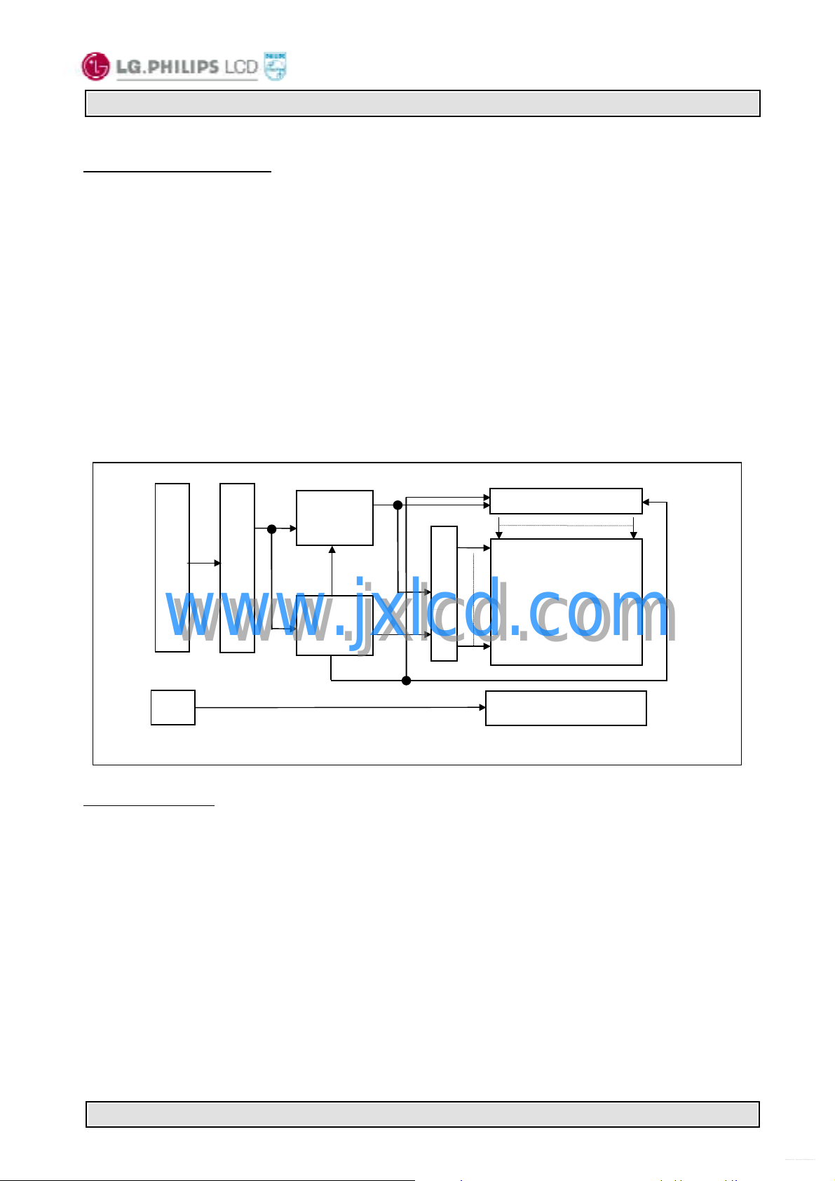
1. General Description
The LP141XB is a Color Active Matrix Liquid Crystal Display with an integral Cold Cathode Fluorescent
Lamp(CCFL) back light system. The m atrix employs a-Si Thin Film Transistor as the active elem ent. It is a
transmissive type display operating in the normally white mode. This TFT-LCD has a 14.1 inc hes diagonally
measured active display area with XGA resolution(768 vertical by 1024 horizontal pixel array). Each pixel is
divided into Red, Green and Blue sub-pixels or dots which ar e arranged in vertical str ipes. Gray scale or the
brightness of the sub-pixel color is determined with a 6-bit gray scale signal for each dot, thus, pres enting a
palette of more than 262,144 colors.
The LP141XB has been designed to apply the interface method that enables low power, high speed, low EMI.
Flat Link must be used as a LVDS(Low Voltage Differential Signaling) chip.
The LP141XB is intended to support applications where thin thickness, low power are critical factors and
graphic displays are important. In com bination with the vertical arrangement of the sub-pix els, the LP141XB
characteristics provide an excellent flat panel display for office automation products such as Notebook PC.
Timing
Control
Block
CN1
www.jxlcd.com
www.jxlcd.com
CN2
FlatLink interface
Power
Block
Row Driver circuit
Column driver circuit
TFT-LCD
(1024×768)
Backlight Ass’y
General Features
Active screen size 14.1 inches(35.814cm) diagonal
Outline dimensions 298.5(H) × 227(V) × 5.5(D) mm (Typ.)
Pixel pitch 0.279 mm × 0.279 mm
Pixel format 1024 horiz. by 768 vert. pixels
RGB stripe arrangement
Color depth 6-bit, 262,144 colors
Luminance, White 160 cd/m
Power Consumption Total 4.73Watt(Typ.)
Weight 485g (Typ.)
Display operating mode Transmissive mode, normally white
Surface treatments Hard coating (3H),
Anti-glare treatment of the front polarizer
2
(Typ.)
Ver 0.5 Apr 19, 2001 Page 4/24
Page 5
www.DataSheet.net/
Datasheet pdf - http://www.DataSheet4U.co.kr/
Product Specification
LP141XB
Liquid Crystal Display
2. Absolute Maximum Ratings
The following are maximum values which, if exceeded, may cause faulty operation or damage to the unit.
Table 1 ABSOLUTE MAXIMUM RATINGS
Parameter Symbol
Power Input Voltage
Operating Temperature
Storage Temperature
Operating Ambient Humidity
Storage Humidity
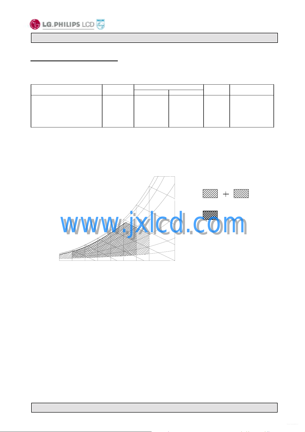
Note: 1. Temperature and relative humidity range are shown in the figure below.
Wet bulb temperature should be 39℃ Max, and no condensation of water.
V
CC
T
OP
T
ST
H
OP
H
ST
Values
Min. Max.
-0.3
0
-20
10
10
4.0
50
60
90
90
Units Notes
%RH
%RH
Vdc
℃
℃
at 25 ±5℃
1
1
1
1
Wet Bulb
Temperature [℃]
30
www.jxlcd.com
www.jxlcd.com
10
0
-20
10
Dry Bulb Temperature [℃]
20
20 30 40 50
40
50
60
60 70 80 0
95% 80%
60
40
20
10
%
%
%
Humidity [(%)RH]
%
Storage
Operation
Ver 0.5 Apr 19, 2001 Page 5/24
Page 6
www.DataSheet.net/
Datasheet pdf - http://www.DataSheet4U.co.kr/
Product Specification
LP141XB
Liquid Crystal Display
3. Electrical Specifications
3-1. Electrical Characteristics
The LP141XB requires two power inputs. One is employed to power the LCD electronics and to drive the
TFT array and liquid crystal. The second input which powers the CCFL, is typically generated by an inverter.
The inverter is an external unit to the LCD.
Table 2 ELECTRICAL CHARACTERISTICS:
Parameter Symbol Values Units Notes
Min. Typ. Max.
MODULE:
Power Supply Input Voltage
Power Supply Input Current
Differential Impedance
Power Consumption
Rush Current
Duration of rush current
LAMP
Operating Voltage
Operating Current
Established Starting Voltage
at 25℃
at 0℃
Operating Frequency
Discharge Stabilization Time
Power Consumption
Life Time
Note)The design of the inverter must have specifications for the lamp in LCD Assembly.
The performance of the Lamp in LCM, for example life time or brightness, is extremely influenced by the
characteristics of the DC-AC Inverter. So all the parameters of an inverter should be carefully designed
so as not to produce too much leakage current from high-voltage output of the inverter.
When you design or order the inverter, please make sure unwanted lighting caused by the mismatch of
the lamp and the inverter(no lighting, flicker, etc) never occurs. When you confirm it, the LCD Assembly
should be operated in the same condition as installed in your instrument.
Notes: 1. The specified current and power consumption are under the Vcc = 3.3V , 25℃, fv = 60Hz condition
whereas full black pattern is displayed and fv is the frame frequency.
2. This impedance value is needed to proper display and measured from LVDS Tx to the mating
connector.
3. The specified rush current and duration of rush current are under the Vcc = 3.3V,
Current limit = 1.6A, 25℃, fv = 60Hz condition whereas full black pattern is displayed and fv is the
frame frequency. The duration of rush current is about 20ms.
4. The variance of the voltage is ±10%.
5. The voltage above V
6. The output of the inverter must have symmetrical(negative and positive) voltage waveform and
symmetrical current waveform.(Unsymmetrical ratio is less than 10%) Please do not use the inverter
which has unsymmetrical voltage and unsymmetrical current and spike wave. Lamp frequency may
produce interference with horizontal synchronous frequency and as a result this may cause beat on
the display. Therefore lamp frequency shall be as away as possible from the horizontal synchronous
frequency and from its harmonics in order to prevent interference.
www.jxlcd.com
www.jxlcd.com
should be applied to the lamps for more than 1second for start-up.
s
Otherwise, the lamps may not be turned on.
V
I
Z
I
RUSH
T
RUSH
CC
CC
Pc
V
IL
V
F
T
PL
m
L
s
L
s
3.0
-
90
-
-
-
680(6mA)
3.0
-
-
45
-
10,000
3.3
0.335
100
1.1
1.0
-
725(5mA)
5.0
-
-
58
3.63
3.6
0.370
110
1.22
1.5
30
875(3mA)
6.0
1170
1450
80
3
4.08
-
Vdc
A
Ohm
W
A
ms
V
rms
MA
rms
V
rms
V
rms
kHz
Minutes
W
Hours
1
2
1
3
3
4
5
6
7
8
6mA
Ver 0.5 Apr 19, 2001 Page 6/24
Page 7
www.DataSheet.net/
Datasheet pdf - http://www.DataSheet4U.co.kr/
Product Specification
7.Let’s define the brightness of the lamp after being lighted for 5 minutes as 100%.
T
8. The lamp power consumption shown above does not include loss of external inverter. The used
lamp current is the lamp typical current.
9. The life is determined as the time at which brightness of lamp is 50% compared to that of initial value
at the typical lamp current on condition of continuous operating at 25 ±2℃.
10. Do not attach a conducting tape to lamp connecting wire. If conducting tape is attached to lamp wire,
TFT-LCD Module can have low luminance and the inverter can have abnormal action because of
leakage current.
is the time required for the brightness of the center of the lamp to be not less than 95%.
s
LP141XB
Liquid Crystal Display
3-2. Interface Connections
This LCD employs two interface connections, a 20 pin connector is used f or the module electronics and the
other connector is used for the integral backlight system.
The electronics interface connector is a model GT122-20P-H13R manufactured by LG Cable. The pin
configuration for the connector is shown in the table below.
Pin Symbol Description Notes
1
2
3
4
5
6
7
8
9
10
11
12
13
14
15
16
17
18
19
20
The backlight interfac e connector is a model BHSR-02VS-1, m anufactured by JST. The mating connec tor
part number is SM02B-BHSS-1 or equivalent. The pin conf iguration for the connector is shown in the table
below.
Table 4 BACKLIGHT CONNECTOR PIN CONFIGURATION
Notes: 1. The high voltage side terminal is colored pink. The low voltage side terminal is black.
Table 3 MODULE CONNECTOR PIN CONFIGURATION (LVDS) [CN1]
Vcc
Vcc
GND
GND
A0M
A0P
www.jxlcd.com
GND
www.jxlcd.com
A1M
A1P
GND
A2M
A2P
GND
CLKM
CLKP
GND
NC
NC
GND
GND
Pin Symbol Description Notes
1
2
Differential Signal
Differential Signal
Differential Signal
Differential Signal
Differential Signal
Differential Signal
Differential Signal
Differential Signal
No Connection
No Connection
Power (3.3V)
Power (3.3V)
Ground
Ground
Ground
Ground
Ground
Ground
Ground
Ground
HV
LV
1. Interface chips
1.1 LCD : SN75LVDS88B (TI)
(SN75LVDS86 core + Timing Controller)
1.2 System : SN75LVDS84(TI)
* Pin to Pin compatible with TI LVDS
2. Connector
2.1 LCD : GT122-20P-H13 R (LG Cable)
2.2 Mating : FI-SE20M (JAE) or compatible
2.3 Connector pin arrangement
Viewing on Display side
Power supply for lamp
(High voltage side)
Power supply for lamp
(Low voltage side)
1 … 20
CN1
CN2
1
1
Ver 0.5 Apr 19, 2001 Page 7/24
Page 8
www.DataSheet.net/
Datasheet pdf - http://www.DataSheet4U.co.kr/
Product Specification
Table 5 REQUIRED SIGNAL ASSIGNMENT FOR FlatLink Transmitter
Pin # Pin Name Require Signals Pin # Pin Name Require Signals
1 D4 R4 48 D3 R3
2 Vcc Vcc 47 D2 R2
3 D5 R5 46 GND GND
4 D6 G0 45 D1 R1
5 GND GND 44 D0 R0
6 D7 G1 43 NC NC
7 D8 G2 42 LVDS GND LVDS GND
8 Vcc Vcc 41 Y0M A0M
9 D9 G3 40 Y0P A0P
10 D10 G4 39 Y1M A1M
11 GND GND 38 Y1P A1P
12 D11 G5 37 LVDS Vcc LVDS Vcc
13 D12 B0 36 LVDS GND LVDS GND
14 NC NC 35 Y2M A2M
15 D13 B1 34 Y2P A2P
16 D14 B2 33 CLKOUTM CLKM
17 GND GND 32 CLKOUTP CLKP
18 D15 B3 31 LVDS GND LVDS GND
19 D16 B4 30 PLLGND PLL GND
20 D17 B5 29 PLLVcc PLL Vcc
21 Vcc Vcc 28 PLLGND PLL GND
22 D18 HSYNC 27 SHDN SHDN
23 D19 VSYNC 26 CLKIN Dclk
24 GND GND 25 D20 DE(Data Enable)
www.jxlcd.com
www.jxlcd.com
LP141XB
Liquid Crystal Display
Notes : Refer to LVDS Transmitter Data Sheet for detail descriptions.
Ver 0.5 Apr 19, 2001 Page 8/24
Page 9

www.DataSheet.net/
Datasheet pdf - http://www.DataSheet4U.co.kr/
Product Specification
LP141XB
Liquid Crystal Display
3-3. Signal Timing Specifications
This is the signal timing required at the input of the LVDS Transmitter. All of the interface signal timing
s hould be s atis f ied with the following spec if ic ations f or it’s proper operation.
Table 6 Timing Table
ITEM SYMBOL MIN. Typ. MAX. UNIT NOTE
Frequency fCLK 62 65 68 MHz
Dclk Width-Low t
Width –High t
Period tHP 1196 1344 1364
Hsync Width tWH 8 136 240
Active Period t
Period tVP 780 806 830
Vsync Width tWV 1 6 24
Active Period t
Set up Time tSI 5 - - ns for Dclk
Hold Time tHI 5 - -
Horizontal tHBP 10 160
www.jxlcd.com
Back Porch t
DTMG Horizontal tHFP 10 24
(DE) Front Porch
Vertical tVBP 2 29
Back Porch tHP
www.jxlcd.com
3 - -
WCL
3 - -
WCH
1024 1024 1024
WHA
768 768 768
WVA
CLK
Vertical tVFP 1 3
Front Porch
Set up Time tSD 5 - - ns for Dclk
DATA Hold Time tHD 5 - -
* The Maximum Dclk jitter is 2.0nsec.
Ver 0.5 Apr 19, 2001 Page 9/24
Page 10

V
www.DataSheet.net/
Datasheet pdf - http://www.DataSheet4U.co.kr/
3-4. Signal Timing Waveforms
Dclk,Hsync, Vsync, DTMG, DATA
t
Dclk
tSD
Product Specification
t
t
WCH
t
HD
V
=0.7VDD
H
=0.3VDD
LP141XB
Liquid Crystal Display
DATA Invalid Data
DTMG
DTMG
DTMGDTMG
tttt
WH
WH
WHWH
Hsyn
DTM
Vsync
DTM
www.jxlcd.com
www.jxlcd.com
tttt
WV
WV
WVWV
t
t
VBP
HBP
Invalid Data
t
S
IIII
t
t
HP
t
WHA
tttt
VP
VP
VPVP
t
WVA
t
HfP
t
VfP
Ver 0.5 Apr 19, 2001 Page 10/24
Page 11

www.DataSheet.net/
Datasheet pdf - http://www.DataSheet4U.co.kr/
LP141XB
Liquid Crystal Display
Product Specification
3-5. Color Input Data Reference
The brightness of each prim ary color(red, green and blue) is based on the 6-bit gray sc ale data input for the
color; the higher the binary input, the brighter the color. The table below provides a reference for color
versus data input.
Table 7 COLOR DATA REFERENCE
Input Color Data
Basic
Colors
Red
Green
Blue
Color Red
MSB LSB
R5 R4 R3 R2 R1 R0 G5 G4 G3 G2 G1 G0 B5 B4 B3 B2 B1 B0
0
0
Black
Red(63)
Green(63)
Blue(63)
Cyan
Magenta
Yellow
White
Red(00) Dark
Red(01)
Red(02)
Red(61)
Red(62)
Red(63) Bright
Green(00)Dark
Green(01)
Green(02)
Green(61)
www.jxlcd.com
Green(62)
www.jxlcd.com
Green(63)Bright
Blue(00) Dark
Blue(01)
Blue(02)
Blue(61)
Blue(62)
Blue(63) Bright
0
1
0
0
0
1
1
1
0
0
0
:
1
1
1
0
0
0
:
0
0
0
0
0
0
:
0
0
0
0
0
1
1
1
1
0
0
0
0
0
0
0
0
0
0
0
0
1
1
1
1
1
1
1
1
1
1
1
1
0
0
0
0
0
0
0
0
1
0
0
0
:
:
:
:
0
1
1
1
1
1
1
1
1
1
1
1
0
0
0
0
0
0
0
0
0
0
0
0
:
:
:
:
0
0
0
0
0
0
0
0
0
0
0
0
0
0
0
0
0
0
0
0
0
0
0
0
:
:
:
:
0
0
0
0
0
0
0
0
0
0
0
0
MSB LSB
0
0
0
1
1
0
0
0
1
0
0
1
1
1
1
1
0
0
0
1
0
0
:
:
0
1
0
0
0
1
0
0
0
0
0
0
:
:
1
0
1
0
1
0
0
0
0
0
0
0
:
:
0
0
0
0
0
0
0
0
1
0
1
0
1
1
0
0
0
:
0
0
0
0
0
0
:
1
1
1
0
0
0
:
0
0
0
Green
0
0
0
0
1
1
0
0
1
1
0
0
1
1
1
1
0
0
0
0
0
0
:
:
0
0
0
0
0
0
0
0
0
0
0
0
:
:
1
1
1
1
1
1
0
0
0
0
0
0
:
:
0
0
0
0
0
0
Blue
MSB LSB
0
0
0
0
0
0
0
0
0
0
0
0
0
0
0
0
0
0
0
0
0
0
1
1
1
1
1
1
1
1
0
0
1
1
1
1
1
1
1
1
1
1
1
1
1
1
0
0
0
0
0
0
0
0
1
1
1
1
1
1
1
1
1
1
0
0
0
0
0
0
0
0
0
0
0
0
0
0
0
0
0
0
0
0
0
0
0
0
:
:
:
:
:
:
:
:
0
0
0
0
0
0
0
0
0
0
0
0
0
0
0
0
0
0
0
0
0
0
0
0
0
0
0
0
0
0
0
0
0
0
0
0
0
0
1
0
0
0
0
0
0
0
0
1
:
:
:
:
:
:
:
:
0
0
0
0
0
0
1
0
0
0
0
0
0
0
0
1
0
0
0
0
0
0
1
1
0
0
0
0
0
0
0
0
1
0
0
0
0
0
0
0
0
1
0
0
0
0
0
0
:
:
:
:
:
:
:
:
1
0
1
1
1
1
0
0
0
1
1
1
1
1
0
0
1
1
1
1
1
1
0
0
Ver 0.5 Apr 19, 2001 Page 11/24
Page 12

www.DataSheet.net/
Datasheet pdf - http://www.DataSheet4U.co.kr/
3-6. Power Sequence
Power Supply For LCD
V
Interface Signal,
V
(LVDS Signal of Transmitter)
Power for Lamp
CC
i
0V
0V
0V0V
90%
90%
90%90%
10%
10%10%
0V
0V
0V0V
OFF
OFF
OFFOFF
Product Specification
TTTT
2222
TTTT
1111
Vali
Valid
ValiVali
TTTT
3333
LAMP ON
LAMP ON
LAMP ONLAMP ON
d
d d
LP141XB
Liquid Crystal Display
90%
90%
90%90%
10%
10% 10%
10%10%
TTTT
TTTT
6666
TTTT
5555
TTTT
4444
OFF
OFF
OFFOFF
7777
Parameter Values Units
Min. Typ. Max.
T
T
T
T
T
T
T
Notes: 1. Please avoid floating state of interface signal at invalid period.
www.jxlcd.com
1
2
3
4
5
6
7
www.jxlcd.com
2. When the interface signal is invalid, be sure to pull down the power supply for LCD V
3. Lamp power must be turn on after power supply for LCD and interface signal are valid.
0.01
0.01
50
15
0.01
0.01
1
-
-
-
-
-
-
-
10
50
-
50
10
-
ms
ms
ms
ms
ms
ms
s
to 0V.
CC
Ver 0.5 Apr 19, 2001 Page 12/24
Page 13

www.DataSheet.net/
Datasheet pdf - http://www.DataSheet4U.co.kr/
LP141XB
Liquid Crystal Display
Product Specification
4. Optical Specifications
Optical characteristics ar e determined after the unit has been ‘O N’ and stable for approxim ately 30 minutes
in a dark environment at 25℃. The values specified are at an approximate distance 50cm from the LCD
surface at a viewing angle of Φ and θ equal to 0°.
Appendix A -1 presents additional information concerning the measurement equipment and method.
Table 8 OPTICAL CHARACTERISTICS
Parameter Symbol Values Units Notes
Min. Typ. Max.
Contrast Ratio
Surface Luminance, white
Luminance Variation
Response Time
Rise Time
Decay Time
CIE Color Coordinates
Red
Green
Blue
White
Viewing Angle
x axis, right (Φ=0º)
x axis, left(Φ=180º)
y axis, up(Φ=90º)
y axis, down (Φ=270º
www.jxlcd.com
www.jxlcd.com
)
Gray Scale
δ
CR
L
WH
WHITE
Tr
Tr
R
Tr
D
x
R
y
R
x
G
y
G
x
B
y
B
x
W
y
W
θr
θl
θu
θd
150
130
-
-
-
0.562
0.308
0.291
0.521
0.124
0.122
0.308
0.327
40
40
10
30
-
250
160
-
20
30
0.592
0.338
0.321
0.551
0.154
0.152
0.338
0.357
-
-
-
-
-
1.45
40
50
0.622
0.368
0.351
0.581
0.184
0.182
0.368
0.387
Notes 1. Contrast Ratio (CR) is defined mathematically as :
Surface Luminance with all white pixels
Contrast Ratio =
Surface Luminance with all black pixels
2. Surface luminance is the average luminance of 5points across the LCD surface 50cm from
the surface with all pixels displaying white. For more information see Appendix A - 2.
When I
=6mA, LWH= 130cd/m2 (Min.) 160cd/m2 (Typ.)
BL
3. The variation in surface luminance, δWHITE is determined by measuring L
position 1 through 9, and then dividing the maximum L
of 9 points luminance. For more information see Appendix A - 2.
δWHITE = Maximum (L
ON1
, L
ON2
, ....L
ON9
of 9 points luminance by minimum L
ON
) ÷ Minimum (L
4. Response time is the time required for the display to transition from white to black (Rise Time,
) and from black to white (Decay Time, TrD). For additional information see Appendix A - 3.
Tr
R
5. Viewing angle is the angle at which the contrast ratio is greater than 10. The angles are
determined for the horizontal or x axis and the vertical or y axis with respect to the z axis which
is normal to the LCD surface. For more information see Appendix A - 4
( Ta=25℃, Vcc=3.3V, fV =60Hz,
Dclk=65MHz, I
-
-
cd/m
2
BL
ms
PR-650
Only for
Coordinate
-
-
-
-
-
degree
, L
ON1
at each test
ON
, ....L
ON2
=6mA)
1
2
3
4
Color
5
6
)
ON9
ON
6. Gray scale specification.
Ver 0.5 Apr 19, 2001 Page 13/24
Page 14

www.DataSheet.net/
Datasheet pdf - http://www.DataSheet4U.co.kr/
Product Specification
Gray Level
L0 0.4
L7 1.30
L15 5.00
L23 11.0
L31 21.5
L39 35.5
L47 54.5
L55 75.0
L63 100
Luminance(%)
(Typ.)
LP141XB
Liquid Crystal Display
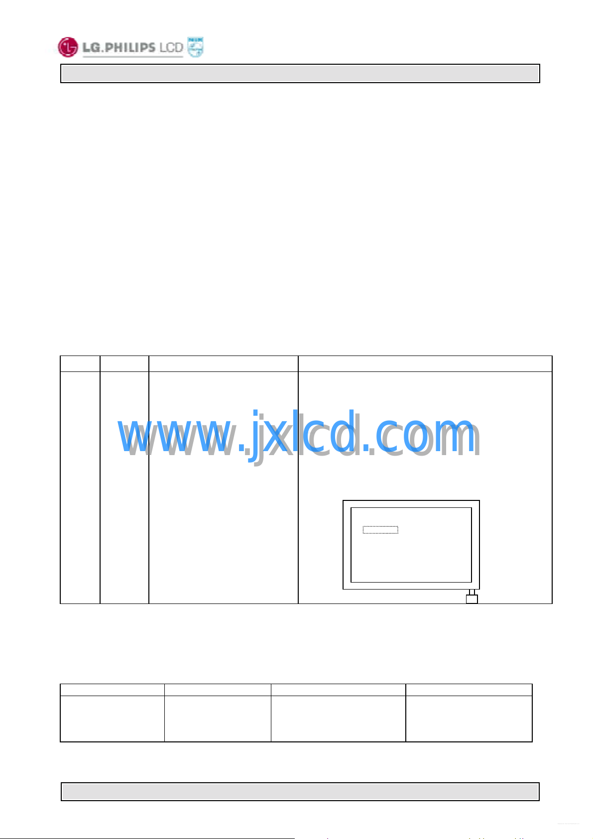
5. Mechanical Characteristics
The contents provide general mechanical characteristics for the model LP141XB LCD. In addition, the
figures in the next page are detailed mechanical drawings of the LCD.
Outside dimensions :
Horizontal 298.5 ±0.5 mm
Vertical 227.0 ±0.5 mm
Bezel area :
Horizontal 288.8 ±0.5 mm
Vertical 217.4 ±0.5 mm
Active Display area :
Horizontal 285.696 mm
Vertical 214.272 mm
Weight (approximate) : 485g (Typ.), 495g(Max.)
Surface Treatment : Hard coating (3H)
Anti-glare treatment of the front polarizer
www.jxlcd.com
www.jxlcd.com
Depth 5.5 ±0.3 mm
(The depth of user connector area : Max. 6.2mm)
< FRONT VIEW >
Ver 0.5 Apr 19, 2001 Page 14/24
Page 15

www.DataSheet.net/
Datasheet pdf - http://www.DataSheet4U.co.kr/
Product Specification
LP141XB
Liquid Crystal Display
www.jxlcd.com
www.jxlcd.com
Note) 1.General Tolerance is ±0.5mm.
2.The depth of user connector area : Max. 6.2mm
3.Due to the thickness (0.2mm) of Sheet, the left side of LCM is not plain.
Ver 0.5 Apr 19, 2001 Page 15/24
Page 16

www.DataSheet.net/
Datasheet pdf - http://www.DataSheet4U.co.kr/
< REAR VIEW >
LP141XB
Liquid Crystal Display
Product Specification
www.jxlcd.com
www.jxlcd.com
Ver 0.5 Apr 19, 2001 Page 16/24
Page 17

www.DataSheet.net/
Datasheet pdf - http://www.DataSheet4U.co.kr/
<Detail description of side mounting screw>
LP141XB
Liquid Crystal Display
Product Specification
www.jxlcd.com
www.jxlcd.com
(Min 1.8)
Ver 0.5 Apr 19, 2001 Page 17/24
Page 18

www.DataSheet.net/
Datasheet pdf - http://www.DataSheet4U.co.kr/
Product Specification
6. Reliability
- Environment test condition
No. Test Item Conditions
LP141XB
Liquid Crystal Display
1 High temperature storage test
2 Low temperature storage test
3 High temperature operation test
4 Low temperature operation test
5 Vibration test
(non-operating)
Shock test
6
(non-operating)
Altitude
7
operating
storage / shipment
{Result Evaluation Criteria}
There should be no change which might affect the practical display function when the display quality
test is conducted under normal operating condition.
- ON/OFF Cycle
: The display module will be capable of being operated over 24,000 ON/OFF cycles (Lamp power &
Vcc ON/OFF)
- Mean Time Between Failure
: The LCD Panel and interface board assembly (excluding the CCFL) have a mean time between
failures of 30,000 hours with a confidence level 90%.
www.jxlcd.com
www.jxlcd.com
Ta = 60℃ 240h
Ta = -20℃ 240h
Ta = 50℃ 50%RH 240h
Ta = 0℃ 240h
Sine wave, 5~100~5Hz, 2G, 1Min/test for 3 axis,
Total: 120 times
55G, 11ms/test for each direction(X,Y,Z)
Total : 5test
0 - 10,000 feet (3,048m)
0 - 40,000 feet (12,192m)
Ver 0.5 Apr 19, 2001 Page 18/24
Page 19

www.DataSheet.net/
Datasheet pdf - http://www.DataSheet4U.co.kr/
Product Specification
7. International Standards
7-1. Safety
a) UL 1950 Third Edition, Underwriters Laboratories, Inc. Jan. 28, 1995.
Standard for Safety of Information Technology Equipment Including Electrical Business
Equipment.
b) CAN/CSA C22.2 No. 950-95 Third Edition, Canadian Standards Association, Jan. 28, 1995.
Standard for Safety of Information Technology Equipment Including Electrical Business
Equipment.
c) EN 60950 : 1992 + A1 : 1993 + A2 : 1993 + A3 : 1995 + A4 : 1997 + A11 : 1997
IEC 950 : 1991 + A1 : 1992 + A2 : 1993 + A3 : 1995 + A4 : 1996
European Committee for Electrotechnical Standardization (CENELEC)
EUROPEAN STANDARD for Safety of Information Technology Equipment Including Electrical
Business Equipment.
LP141XB
Liquid Crystal Display
7-2. EMC
a) ANSI C63.4 “Methods of Measurement of Radio-Noise Emissions from Low-Voltage Electrical
and Electronic Equipment in the Range of 9kHz to 40GHz.” American National Standards
Institute(ANSI),1992.
b) C.I.S.P.R “Limits and Methods of Measurement of Radio Interference Characteristics of
Information Technology Equipment.” International Special Committee on Radio Interference
c) EN 55022 “Limits and Methods of Measurement of Radio Interference Characteristics of
Information Technology Equipment.” European Committee for Electrotechnical
Standardization (CENELEC),1988
www.jxlcd.com
www.jxlcd.com
Ver 0.5 Apr 19, 2001 Page 19/24
Page 20

www.DataSheet.net/
Datasheet pdf - http://www.DataSheet4U.co.kr/
Product Specification
LP141XB
Liquid Crystal Display
8. Packing
8-1. Designation of Lot Mark
a) Lot Mark
A, B ,C : SIZE
D : YEAR
E : MONTH
F,G : PANEL CODE
H : ASSEMBLY CODE
I,J,K,L,M : SERIAL NO.
Note : 1. YEAR
YEAR
Mark
MONTH
Mark
2. MONTH
97
7
Jan. Feb. Mar. Apr. May. Jun. Jul. Aug. Sep. Oct. Nov. Dec.
1
2
98
8
99 2000 2001 2002 2003 2004 2005 2006 2007
9
3
3. Serial No.
www.jxlcd.com
www.jxlcd.com
K J I H G F E D C B A L M
0
1
2
3
4
5
6
7
4
5
6
7
8
9
A
B C
Serial No.
Mark
b) Location of Lot Mark
Serial NO. Is printed on the label. The label is attached to the backside of the LCD module.
This is subject to change without prior notice.
1 ~ 99999
00001 ~ 99999
A0001~A9999, ········ ,Z9999,
100000 ~
8-2. Packing Form
a) Package quantity in one box : 10 pcs
b) Box Size : 371 X 239 X 300 mm
Ver 0.5 Apr 19, 2001 Page 20/24
Page 21

www.DataSheet.net/
Datasheet pdf - http://www.DataSheet4U.co.kr/
Product Specification
LP141XB
Liquid Crystal Display
9.PRECAUTIONS
Please pay attention to the followings when you use this TFT LCD module.
9.1 MOUNTING PRECAUTIONS
(1) You must mount a module using holes arranged in four corners or four sides.
(2) You should consider the mounting structure so that uneven force (ex. twisted stress) is not applied
to the module.
And the case on which a module is mounted should have sufficient strength so that external
force is not transmitted directly to the module.
(3) Please attach a transparent protective plate to the surface in order to protect the polarizer.
Transparent protective plate should have sufficient strength in order to resist external force.
(4) You should adopt radiation structure to satisfy the temperature specification.
(5) Acetic acid type and chlorine type materials for the cover case are not desirable because the former
generates corrosive gas of attacking the polalizer at high temperature and the latter causes circuit
break by electro-chemical reaction.
(6) Do not touch, push or rub the exposed polarizers with glass, tweezers or anything harder than HB
pencil lead. And please do not rub with dust clothes with chemical treatment.
Do not touch the surface of polarizer for bare hand or greasy cloth. (Some cosmetics are
detrimental to the polarizer.)
(7) When the surface becomes dusty, please wipe gently with absorbent cotton or other soft materials
like chamois soaked with petroleum benzene. Normal-hexane is recommended for cleaning the
adhesives used to attach front / rear polarizers. Do not use acetone, toluene and alcohol because
they cause chemical damage to the polarizer.
(8) Wipe off saliva or water drops as soon as possible. Their long time contact with polarizer causes
deformations and color fading.
(9) Do not open the case because inside circuits do not have sufficient strength.
www.jxlcd.com
www.jxlcd.com
9.2 OPERATING PRECAUTIONS
(1) The spike noise causes the mis-operation of circuits. It should be lower than following voltage :
V = ± 200mV (Over and under shoot voltage).
(2) Response time depends on the temperature. (In lower temperature, it becomes longer.)
(3) Brightness depends on the temperature. (In lower temperature, it becomes lower.)
And in lower temperature, response time (required time that brightness is stable after turned on )
becomes longer.
(4) Be careful for condensation at sudden temperature change. Condensation makes damage to
polarizer or electrical contacted parts. And after fading condensation, smear or spot will occur.
(5) When fixed patterns are displayed for a long time, remnant image is likely to occur.
(6) Module has high frequency circuits. Sufficient suppression to the electromagnetic interference
shall be done by system manufacturers. Grounding and shielding methods may be important to
minimize the interference.
Ver 0.5 Apr 19, 2001 Page 21/24
Page 22

www.DataSheet.net/
Datasheet pdf - http://www.DataSheet4U.co.kr/
Product Specification
LP141XB
Liquid Crystal Display
9.3 ELECTROSTATIC DISCHARGE CONTROL
Since a module is composed of electronic circuits, it is not strong to electrostatic discharge. Mak e certain
that treatment persons are connected to ground through wrist band etc . And don’t touch interface pin directly.
9.4 PRECAUTIONS FOR STRONG LIGHT EXPOSURE
Strong light exposure causes degradation of polarizer and color filter.
9.5 STORAGE
When storing modules as spares for a long time, the following precautions are necessary.
(1) Store them in a dark place. Do not expose the module to sunlight or fluorescent light. Keep the
temperature between 5℃ and 35℃ at normal humidity.
(2) The polarizer surface should not come in contact with any other object.
It is recommended that they be stored in the container in which they were shipped.
9.6 HANDLING PRECAUTIONS FOR PROTECTION FILM
(1) When the protection film is peeled off, static electricity is generated between the film and polarizer.
This should be peeled off slowly and carefully by people who are electrically grounded and with well
ion- blown equipment or in such a condition, etc.
(2) The protection film is attached to the polarizer with a small amount of glue. If some stress is applied
to rub the protection film against the polarizer during the time you peel off the film, the glue is apt to
remain on the polarizer.
Please carefully peel off the protection film without rubbing it against the polarizer.
(3) When the module with protection film attached is stored for a long time, sometimes there remains a
very small amount of glue still on the polarizer after the protection film is peeled off.
(4) You can remove the glue easily. When the glue remains on the polarizer surface or its vestige is
recognized, please wipe them off with absorbent cotton waste or other soft material like chamois
soaked with normal-hexane.
www.jxlcd.com
www.jxlcd.com
Ver 0.5 Apr 19, 2001 Page 22/24
Page 23

www.DataSheet.net/
Datasheet pdf - http://www.DataSheet4U.co.kr/
Product Specification
LP141XB
Liquid Crystal Display
A-1 Optical Characteristic Measurement Equipment and Method
Optical Stage(x,y)
LCD Module
Field = 1°
500mm
Pritchard 880 or
equivalent
A-2 Luminance
<measuring point for luminance variation> <measuring point for surface luminance >
768
2222
8888
5555
768 512
768768
3333
6666
9999 7777
192
192
192192
384
384
384384
576
576
576576
256
256256
2222
512 256
512512
1111
256
256256
www.jxlcd.com
512 256
512512
1111
www.jxlcd.com
4444
A-3 Response Time
The response time is defined as the following figure and shall be measured by
switching the input signal for “black” and “white”.
Tr
D
Optical
100
90
Tr
%
R
768
768 512
768768
3333
5555 4444
192
192
192192
384
384
384384
576
576
576576
Response
10
Ver 0.5 Apr 19, 2001 Page 23/24
white
0
black
white
Page 24

www.DataSheet.net/
Datasheet pdf - http://www.DataSheet4U.co.kr/
A-4 Viewing angle
<Definition of viewing angle range>
= 0。
θ
= 90。
φ
yu
(12:00)
=
。
φ
180
xl
(9:00)
z
Product Specification
A
θ
φ
= 0。
φ
(3:00)
LP141XB
Liquid Crystal Display
xr
TFT LCD
MODULE
www.jxlcd.com
www.jxlcd.com
z' yd
= 270。
φ
(6:00)
Ver 0.5 Apr 19, 2001 Page 24/24
 Loading...