

Page 1
www.DataSheet4U.com
( DataSheet : www.DataSheet4U.com )
LG LCD Inc.
( ) Preliminary Specification
Product Specification
SPECIFICATION
For
APPROVAL
LP141XA-A1
Li
quid Crystal Display
( ) Final Specification
Title 14.1” XGA TFT LCD
BUYER NAME PC OBU SUPPLIER LG LCD Inc.
MODEL NAME MODEL NAME LP141XA-A1
www.jxlcd.com
www.jxlcd.com
SIGNATURE DATE SIGNATURE DATE
APPROVED BY
S. H. Kang
REVIEWED BY
S. C. YUN
B. H. KOO
PREPARED BY
Please return 1 copy for our confirmation
with your signature and comments.
+
Version 1.4 08 / Jul. / 1999 Page 1/19
H. S. SONG
S. J. LEE
Product Engineering Dept.
LG LCD Inc.
Page 2

LG LCD Inc.
Product Specification
LP141XA-A1
Li
quid Crystal Display
TABLE of CONTENTS
NO. ITEM Page
-
- TABLE of CONTENTS 2/19
- RECORD of REVISION 3/19
1. GENERAL DESCRIPTION 4/19
2. MAXIMUM RATINGS 5/19
3. ELECTRICAL SPECIFICATIONS 5/19
4. OPTICAL SPECIFICATIONS 6/19
5. INTERFACE CONNECTIONS 7/19
6. SIGNAL TIMING SPECIFICATIONS 9/19
7. SIGNAL TIMING WAVE FORMS 10/19
8. COLOR INPUT DATA REFERENCE 12/19
9. POWER SEQUENCE 13/19
10. MECHANICAL CHARACTERISTICS 14/19
11. HANDLING PRECAUTIONS 16/19
12. INTERNATIONAL STANDARDS 17/19
www.jxlcd.com
www.jxlcd.com
- APPENDIX 18/19
COVER 1/19
Version 1.4 08 / Jul. / 1999 Page 2/19
Page 3
LG LCD Inc.
Product Specification
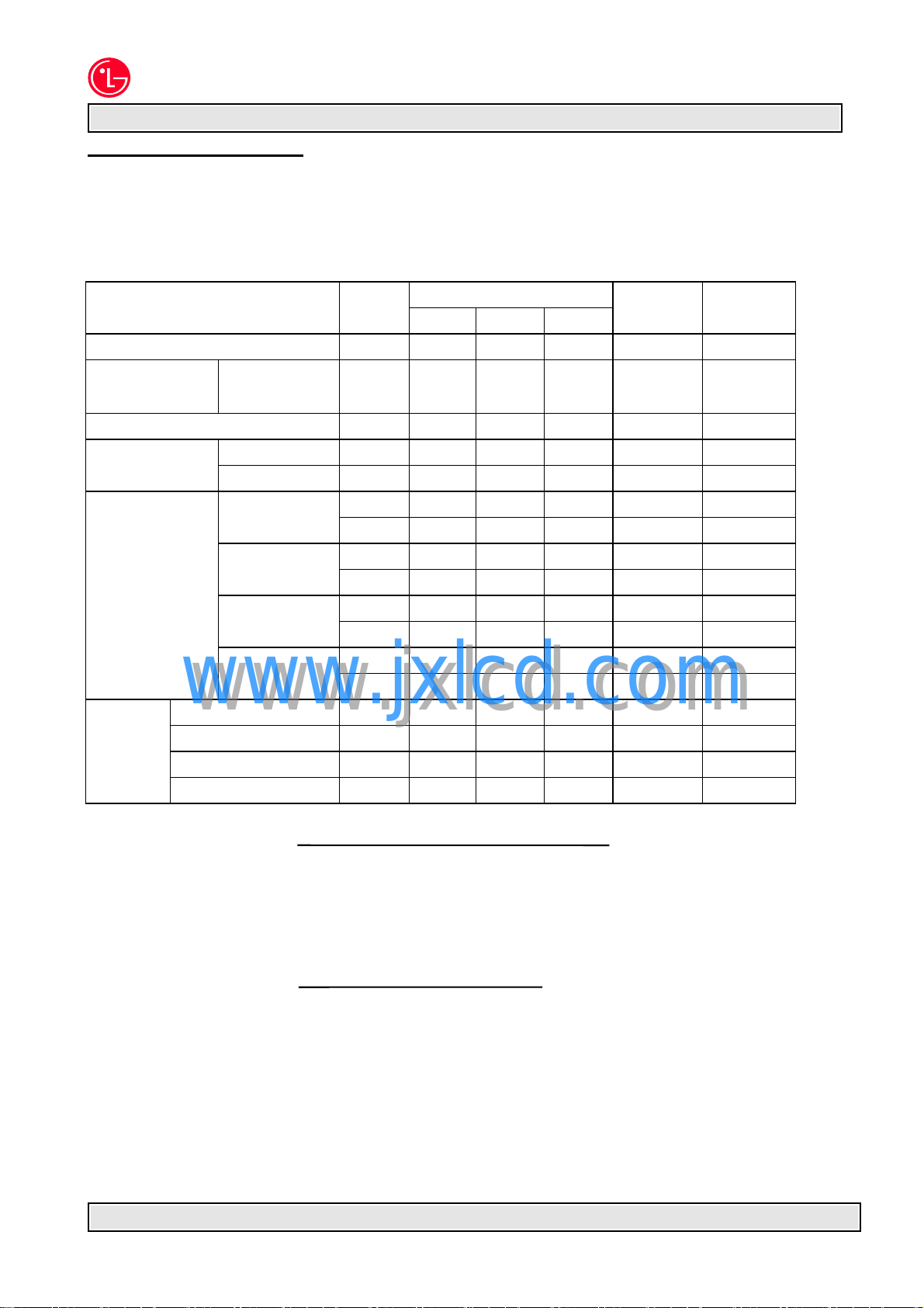
Record of Revision
DATE AND VERSION DESCRIPTION
LP141XA-A1
Li
quid Crystal Display
22 / Jan. / 1999 & Ver. 1.0
12 / Feb. / 1999 & Ver. 1.1
12 / Apr. / 1999 & Ver. 1.2
www.jxlcd.com
28 / May / 1999 & Ver. 1.3
www.jxlcd.com
Initial Release
1. To Change Model Name (All Page)
LP141X4-C1 → LP141XA-A1
2. To change Power supply current (5 Page)
: Typ Max Typ Max
375 510 → 410 570 [mA]
3. To add International Standards (17 Page)
1. To Changed Color Coordinates (6 Page)
: Min. Typ Max Min. Typ Max
① Rx 0.542 0.572 0.602 → 0.548 0.578 0.608
② Ry 0.320 0.350 0.380 → 0.317 0.347 0.377
③ Gx 0.267 0.297 0.327 → 0.278 0.308 0.338
④ Gy 0.519 0.549 0.579 → 0.507 0.537 0.567
⑤ Bx 0.122 0.152 0.182 → 0.121 0.151 0.181
⑥ By 0.110 0.140 0.170 → 0.101 0.131 0.161
⑦ Wy 0.271 0.301 0.331 → 0.281 0.311 0.341
⑧ Wy 0.312 0.342 0.372 → 0.311 0.341 0.371
1. To change Power Sequence (13 Page)
08 / Jul. / 1999 & Ver. 1.4
Lamp On Time : 200[mS] min. → 50[mS] min.
1. Update Mechanical Drawing(14, 15 Page)
2. Change Power Sequence (13 Page)
VDD off time : 20 [mS] max. → 40 [mS] max.
Version 1.4 08 / Jul. / 1999 Page 3/19
Page 4
(
)
r
y
(
)
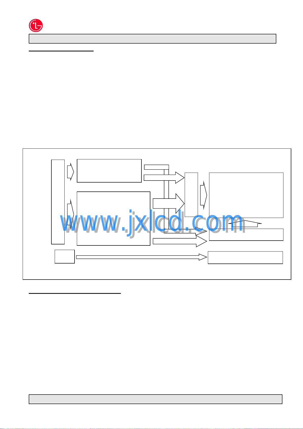
1. General Description
The LG LCD Inc. model LP141XA-A1 LCD is a Color Active Matrix Liquid Crystal Display with an integral
Cold Cathode Fluorescent Tube(CCFT) back light system. The matrix employs a - Si Thin Film Transistor
as the active element. It is a transmissive type display operating in the normally white mode. This TFT-
LCD has a 14.1 inch diagonally measured active display area with XGA resolution(768 vertical by 1024
horizontal pixel array). Each pixel is divided into Red, Green and Blue sub-pixels or dots which are
arranged in vertical stripes. Gray scale or the brightness of the sub-pixel color is determined with a 6-bit
gray scale signal for each dot, thus, presenting a pallet of more than 262,144 colors.
The LP141XA-A1 LCD is intended to support applications where low power consumption, weight and
thickness are critical factors and graphic displays are important. In combination with the vertical
arrangement of the sub-pixels, the LP141XA-A1 characteristics provide an excellent flat panel display for
office automation products such as portable computers.
LG LCD Inc.
Product Specification
LP141XA-A1
Li
quid Crystal Display
Power Supply
VDD
GND
Rin0 -
Rin0 +
Rin1 -
Rin1 +
Rin2 -
Rin2 +
CLK -
CLK +
CN1
LVDS Receiver
Control
Signal
14.1 inch XGA
1024 x RGB x 768
Row Drive
+
www.jxlcd.com
www.jxlcd.com
User Connector
Timing Controller
Column Driver
Data & Control Signal
CN2
General Display Characteristics
The following are general feature of the model LP141XA-A1 LCD;
Active display area
Outsize dimensions
Pixel pitch
Pixel format
Color depth
Display operating mode
Version 1.4 08 / Jul. / 1999 Page 4/19
Surface treatment
14.1 inch diagonal
298.5 W x 227.5 H x 5.8 D mm Typ.
0.279 mm x 0.279 mm
1024 horiz. By 768 vert. pixels
RGB stripe arrangement
transmissive mode, normally white
anti-glare treatment of the front polarizer
hard coating(3H),
Back light Assembl
6-bit
Page 5
LG LCD Inc.
Product Specification
LP141XA-A1
Li
quid Crystal Display
2. Maximum Ratings
The following are maximum values which, if exceeded, may cause faulty operation or damage to the unit.
Table 1 ABSOLUTE MAXIMUM RATINGS
Parameter symbol Values Units Notes
Min. Max.
Power Input Voltage
Logic Input Voltage
Operating Temperature
Storage Temperature
Note: 1. The Relative Humidity must not exceed 80% non-condensing at temperatures of 40℃ or less.
At temperatures greater than 40℃, the wet bulb temperature must not exceed 39℃.
At low temperature the brightness of CCFL drop and the life time of CCFL become to be short.
2. Under no condition should the unit be exposed to corrosive chemicals.
V
DD
V
L/H
TOP
TST
0
-0.3
0
-20
4.0
VDD+0.3
+50
+60
Vdc
Vdc
℃
℃
at 25℃
at 25℃
1
1
3. Electrical Specifications
The LP141XA-A1 requires two power inputs. One is employed to power the LCD electronics and to
derive the voltages to drive the TFT array and liquid crystal. The second input which powers the backlight
CCFT, is typically generated by an inverter. The inverter is an external unit to the LCD.
Parameter Symbol Values Units Notes
Min. Typ. Max.
MODULE:
Power Supply Input Voltage
Power Supply Input Current
Ripple/Noise
Differential input voltage - High
for receiver threshold Low
BACKLIGHT
Backlight Input voltage
Backlight Current
Established starting Voltage
Operating Frequency
CCFL Life Time
Notes 1. The current draw and power consumption specified is for 3.3 Vdc at 25℃.
2.Typical value is measured when displaying black screen.
Maximum power situation measured with alternating vertical lines by 2 black_white pattern.
For more information see Appendix A-1.
3. LVDS common mode voltage, VCM=1.2V
5. The voltage of inverter is more than the established starting voltage.
www.jxlcd.com
www.jxlcd.com
4. The backlight power consumption shown above does not include loss of external inverter.
Table 2 ELECTRICAL CHARACTERISTICS:
V
DD
I
DD
-
V
IH
V
IL
V
BL
I
BL
F
BL
3.0
-
-
-
-100
680
3.0
40
10,000
3.3
410
60
-
-
725
5.0
60
3.6
570
100
100
-
850
6.0
1170
1450
80
Vdc
mA
mV
mV
mV
V
RMS
mA
V
RMS
V
RMS
KHz
Hours
1,2
3
4
25±2℃, 5
0℃
@ I
BL= 6mA
Version 1.4 08 / Jul. / 1999 Page 5/19
Page 6
LG LCD Inc.
Product Specification
LP141XA-A1
Li
quid Crystal Display
4. Optical Specifications
Optical characteristics are determined after the unit has been ‘ON’ and stable for approximately 30 minutes
in a dark environment at 25℃. The values specified are at an approximate distance 50cm from the LCD
surface at a viewing angle of Φ and θ equal to 0°.
Appendix A presents additional information concerning the specified characteristics.
Table 3 OPTICAL CHARACTERISTICS
, ....B
, ....B
Values
)
ON13
)
ON13
ON
Parameter Symbol
Contrast Ratio CR 150 250 - - 1
White Surface
Brightness
Brightness Variation SBV - - 1.80 3
Response Time
Color Coordinates
www.jxlcd.com
www.jxlcd.com
Viewing
Angle
(CR>10:1)
Notes 1. Contrast Ratio (CR) is defined mathematically as:
(Surface Brightness with all white pixels)
(Surface Brightness with all black pixels)
2. Surface brightness is 5 spot average of measurement across the LCD surface 50cm from the
3. The variation in surface brightness, SB
position 1 through 13, and then dividing the maximum B
For more information see Appendix A-3.
Maximum (B
Minimum (B
4. Response time is the time required for the display to transition from white to black
(Rise Time, Tr
For additional information see Appendix A-4.
5. Viewing angle is the angle at which the contrast ratio is greater than 10. The angles are
6. Color Coordinates can be changed according to color filter. (In case of changing color filter,
we will tell our customer.)
x axis, right (Φ =0ٛ) θ
x axis, left(Φ =180ٛ) θ
y axis, up(Φ =90ٛ) θ
y axis, down (Φ =270ٛ) θ
surface with all pixels displaying white. For more information see Appendix A-2.
determined for the horizontal or x axis and the vertical or y axis with respect to the z axis which is
normal to the LCD surface. For more information see Appendix A-5.
IBL=6.0mA
Rise Time TrR - 20 40 msec
Decay Time Tr
RED
GREEN
BLUE
WHITE
) and from black to white (Decay Time, TrD).
R
SB
WH
D
x 0.548 0.578 0.608 - 6
y 0.317 0.347 0.377 - 6
x 0.278 0.308 0.338 - 6
y 0.507 0.537 0.567 - 6
x 0.121 0.151 0.181 - 6
y 0.101 0.131 0.161 - 6
x 0.281 0.311 0.341 - 6
y 0.311 0.341 0.371 - 6
Min. Typ. Max.
100 120 - cd/m2 2
- 30 50 msec
45 degree 5
45 degree 5
10 degree 5
30 degree 5
is determined by measuring BON at each test
V
, B
ON1
ON2
, B
ON1
ON2
Units Notes
by the minimum BON.
Version 1.4 08 / Jul. / 1999 Page 6/19
Page 7

LG LCD Inc.
Product Specification
LP141XA-A1
Li
quid Crystal Display
5. Interface Connections
This LCD employs two interface connections, a 20 pin connector is used for the module electronics and a
two pin connector is used for the integral backlight system.
The electronics interface connector is a model FI-SEB-20P-HF or equivalent.
The pin configuration for the connector is shown in the table below.
Table 4 MODULE CONNECTOR PIN CONFIGURATION (CN1)
Pin Symbol Description Notes
1 VDD Power supply, 3.3V
2 VDD Power supply, 3.3V
3 GND Ground
4 GND Ground
5 Rin0 - Receiver signal (-)
User Connector
6 Rin0 + Receiver signal (+)
7 GND Ground
8 Rin1 - Receiver signal (-)
9 Rin1 + Receiver signal (+)
10 GND Ground
11 Rin2 - Receiver signal (-)
12 Rin2 + Receiver signal (+)
13 GND Ground
14 CLK - Clock signal (-)
15 CLK + Clock signal (+)
16 GND Ground
17 NC Reserved
18 NC Reserved
19 GND Ground
20 GND Ground
Notes: 1. All GND(ground) pins should be connected together and to GND which should also be connected
to the LCD’s metal frame.
2. All V
Version 1.4 08 / Jul. / 1999 Page 7/19
www.jxlcd.com
www.jxlcd.com
(power input) pins should be connected together.
DD
Pin 1
Viewing on Display side
Pin 20
Page 8

Interface Connections (cont’d)
The backlight interface connector is a model BHSR-02VS-1, manufactured by JST. The mating connector
part number is SM02B-BHSS-1-TB or equivalent. The pin configuration for the connector is shown in the
table below.
Notes: 1. The input power terminal is white
LG LCD Inc.
Product Specification
Table 5 BACKLIGHT CONNECTOR PIN CONFIGURATION (CN2)
Pin Symbol Description Notes
1
2
HV
LV
Lamp power input
Ground
LP141XA-A1
Li
quid Crystal Display
1
2
2. The ground terminal is black.
www.jxlcd.com
www.jxlcd.com
6.
Signal Timing Specification
Version 1.4 08 / Jul. / 1999 Page 8/19
Page 9

This is the characteristics of the interface timing parameters. LVDS input timing and LCD interface timing
diagrams are shown in 7.1 and 7.2
LP141XA-A1 with LVDS transmitter recommend to connect to the Display Enable, Horizontal sync, Vertical
sync, Clock signal from Video signal controller to input of Transmitter simultaneously.
LG LCD Inc.
Product Specification
6.1. Interface Signal Timing
LP141XA-A1
Li
quid Crystal Display
ITEM SIGNAL ITEM SYMBOL MIN. TYP. MAX. UNIT
LVDS Clock Frequency
Timing Period
(Note 1) LVDS Low to High time Transition time LLHT - 0.75 1.5 ns
LVDS High to Low time Transition time LHLT - 0.75 1.5 ns
Set up time, serial bits Receiver Input Strobe Bit 0 t0 -0.4 0 0.3 ns
Receiver Input Strobe Bit 1 t1 1.8 2.2 2.5 ns
Receiver Input Strobe Bit 2 t2 4.0 4.4 4.7 ns
Receiver Input Strobe Bit 3 t3 6.2 6.6 6.9 ns
Receiver Input Strobe Bit 4 t4 8.4 8.8 9.1 ns
Receiver Input Strobe Bit 5 t5 10.6 11 11.3 ns
Receiver Input Strobe Bit 6 t6 12.8 13.2 13.5 ns
LVDS DENA Low width
Transimitter Horizontal Front Porch
Input Horizontal Back Porch
(note 2-4) Vertical Front Porch
www.jxlcd.com
www.jxlcd.com
Vertical Back Porch
fCLKIN
tCLKIN
tWDL
tHFP
tHBP
tVFP
tVBP
- 65 66.6 MHz
15 15.4 - ns
100 - -
0 - -
5 - -
0 - -
4 - -
tCLKIN
tCLKIN
tCLKIN
tH
tH
HD Frequency
Period
Low width
VD Frequency
Period
Low width
Note : 1. Measurement is made at panel side flex connector with dummy 100 ohm termination.
2. Polarities of HD and VD are negative.
3. DENA should always be positive polarity.
4. CLKIN should appear during all invalid period. HD should appear during invalid period of the
frame cycle.
tH
tH
t
WHL
fV
tV
tWVL
- 48.5 55.9 kHz
1100 1340 -
1 - -
- 60 62 Hz
772 809 -
0.5 - -
Version 1.4 08 / Jul. / 1999 Page 9/19
tCLKIN
tCLKIN
tH
tH
Page 10

LG LCD Inc.
7. Signal Timing Wave Forms
7.1. LVDS Timing
CLKIN -
CLKIN +
Link a +
Link a (a = 0,1,2)
Link 0
P0C2
G0
P0C1
R5
P0C7
R4
Link 1
P1C2
B1
P1C1
B0
P1C7
G5
Link 2
www.jxlcd.com
tdp 0
tdp 1
tdp 2
tdp 3
tdp 4
tdp 5
tdp 6
P2C2
www.jxlcd.com
DENA
P2C1
VD
P2C7
HD
V IN -
V IN +
VID
Product Specification
t
CLK
P0C6
R3
P1C6
G4
P2C6
B5
P0C5
R2
P1C5
G3
P2C5
B4
P0C4
R1
P1C4
G2
P2C4
B3
P0C3
P1C3
P2C3
LHLTLLHT
R0
G1
B2
LP141XA-A1
Li
quid Crystal Display
“0” “1”
P0C2 P0C1 P0C7
P1C2 P1C1 P1C7
P2C7 P2C1 P2C2
Typical of all
timing instances
Vdiff = 0 V
VID(H)
0V ± 0.01V
VID(L)
Version 1.4 08 / Jul. / 1999 Page 10/19
Page 11

K
LG LCD Inc.
7.2 LCD Interface Timing
CL
Product Specification
LP141XA-A1
Li
quid Crystal Display
DATA
(R,G,B)
DENA
DENA
HD
DENA
3 2 1
Last Data
1023 Invalid Data Invalid Data
tWDL
First Data
tH = 1/fH
www.jxlcd.com
www.jxlcd.com
tHBPtWHL tHFP
tVBPtWVL tVFP
VD
Line data
HD
VD
tV = 1/fV
3
21
4
767
768
Version 1.4 08 / Jul. / 1999 Page 11/19
Page 12

LG LCD Inc.
Product Specification
LP141XA-A1
Li
quid Crystal Display
8. Color Input Data Reference
The brightness of each primary color(red, green and blue) is based on the 6-bit gray scale data input for the
color; the higher the binary input, the brighter the color. The table below provides a reference for color
versus data input.
Table 6 COLOR DATA REFERENCE
Input Color Data
Color Red Green Blue
R5 R4 R3 R2 R1 R0 G5 G4 G3 G2 G1 G0 B5 B4 B3 B2 B1 B0
Basic
Colors
Red
Green
Blue
Black
Red(00)
Green(00)
Blue(00)
Cyan
Magenta
Yellow
White
Red(63) Black
Red(62)
Red(61)
Red(02)
www.jxlcd.com
Red(01)
Red(00)
Green(63) Black
Green(62)
Green(61)
Green(02)
Green(01)
Green(00)
Blue(63) Black
Blue(62)
Blue(61)
Blue(02)
Blue(01)
Blue(00)
www.jxlcd.com
0
1
0
0
0
1
1
1
0
0
0
:
1
1
1
0
0
0
0
0
0
0
0
0
0
0
0
0
0
0
1
0
0
0
1
1
1
0
0
0
:
1
1
1
0
0
0
0
0
0
0
0
0
0
0
0
0
0
0
1
0
0
0
1
1
1
0
0
0
:
1
1
1
0
0
0
0
0
0
0
0
0
0
0
0
0
0
0
1
0
0
0
1
1
1
0
0
0
:
1
1
1
0
0
0
0
0
0
0
0
0
0
0
0
0
0
0
1
0
0
0
1
1
1
0
0
1
:
0
1
1
0
0
0
0
0
0
0
0
0
0
0
0
0
0
0
1
0
0
0
1
1
1
0
1
0
:
1
0
1
0
0
0
0
0
0
0
0
0
0
0
0
0
0
0
0
1
0
1
0
1
1
0
0
0
0
0
0
0
0
0
0
:
1
1
1
0
0
0
0
0
0
0
0
0
1
0
1
0
1
1
0
0
0
0
0
0
0
0
0
0
:
1
1
1
0
0
0
0
0
0
0
0
0
1
0
1
0
1
1
0
0
0
0
0
0
0
0
0
0
:
1
1
1
0
0
0
0
0
0
0
0
0
1
0
1
0
1
1
0
0
0
0
0
0
0
0
0
0
:
1
1
1
0
0
0
0
0
0
0
0
0
1
0
1
0
1
1
0
0
0
0
0
0
0
0
0
1
:
0
1
1
0
0
0
0
0
0
0
0
0
1
0
1
0
1
1
0
0
0
0
0
0
0
0
1
0
:
1
0
1
0
0
0
0
0
0
0
0
0
0
1
1
1
0
1
0
0
0
0
0
0
0
0
0
0
0
0
0
0
0
0
0
;
1
1
1
0
0
0
1
1
1
0
1
0
0
0
0
0
0
0
0
0
0
0
0
0
0
0
0
0
:
1
1
1
0
0
0
1
1
1
0
1
0
0
0
0
0
0
0
0
0
0
0
0
0
0
0
0
0
:
1
1
1
0
0
0
1
1
1
0
1
0
0
0
0
0
0
0
0
0
0
0
0
0
0
0
0
0
:
1
1
1
0
0
0
1
1
1
0
1
0
0
0
0
0
0
0
0
0
0
0
0
0
0
0
0
1
:
0
1
1
0
0
0
1
1
1
0
1
0
0
0
0
0
0
0
0
0
0
0
0
0
0
0
1
0
:
1
0
1
Version 1.4 08 / Jul. / 1999 Page 12/19
Page 13

V
V
LG LCD Inc.
9. Power Sequence
VDD
0V
10%
Product Specification
90%
10mS max
90%
LP141XA-A1
Li
quid Crystal Display
1 Sec min
10%
20mS max
40mS max
Signals
0
Notes : 1. Please avoid floating state of interface signal at invalid period.
2. When the interface signal is invalid, be sure to pull down the power supply for
LCD V
Lamp ON
0
www.jxlcd.com
www.jxlcd.com
to 0V.
DD
10%
50mS min
10%
10%
200mS
10%
Version 1.4 08 / Jul. / 1999 Page 13/19
Page 14

10. Mechanical Characteristics
The chart below provides general mechanical characteristics for the model LP141XA-A1 LCD. The
surface of the LCD has an anti-glare coating to minimize reflection and a 3H hard coating to reduce
scratching. In addition, the figure below is a detailed mechanical drawing of the LCD. Note that dimension
are given for reference purposes only.
< Front View>
LG LCD Inc.
Product Specification
Outside dimensions Width 298.5 mm typ.
Height 227.5 mm typ.
Thickness 5.8 mm typ.
Active Display area Width 285.7 mm
Height 214.3 mm
Diagonal 14.1 inch
Weight 590 g max.
LP141XA-A1
Li
quid Crystal Display
< Rear View>
www.jxlcd.com
www.jxlcd.com
Version 1.4 08 / Jul. / 1999 Page 14/19
Page 15

LG LCD Inc.
Product Specification
LP141XA-A1
Li
quid Crystal Display
www.jxlcd.com
www.jxlcd.com
11. Handling Precautions
* Mounting Screw depth : 2.0[mm] Min. 2.3[mm] Max.
* Torque : 1.3 ~ 1.5 [kgf· cm]
Version 1.4 08 / Jul. / 1999 Page 15/19
Page 16

Please pay attention to the followings when you use this TFT/LCD module with Back-light unit.
11.1.MOUNTING PREACAUTION
1)You must mount Module using mounting holes arranged on metal frame sides. Be sure to turn off the
power when connecting or disconnecting the circuit.
2) Note that the polarizers are easily damaged. Pay attention not to scratch or press this surface with
any hard object.
3) When the LCD surface become dirty, please wipe it off with a soft material. (ie. cotton ball)
4) Protect the module from the ESD as it may damage the electronic circuit (C-MOS). Make certain that
treatment person’s body are grounded through wrist bend.
5) Do not disassemble the module and be careful not to incur a mechanical shock that might occur
during installation. It may cause permanent damage.
6) Do not leave the module in high temperatures, Particularly in areas of high humidity for a long time.
7) The module not be expose to the direct sunlight.
8) Avoid contact with water as it may a short circuit within the module.
11.2 OPERATING PRECAUTION
1) The spike noise causes the mis-operation of circuits. Be lower the spike noise as follows :
VDD=±200mV, V1=±200mV( Over and under shoot voltage.)
2) Response time depends on the temperature. (In lower temperature, it becomes longer.)
3) Brightness depends on the temperature. (In lower temperature, it becomes lower.) And in lower
temperature, response time (Required time that brightness is stable after turn on)becomes longer.
4) Be careful for condensation at suddern temperature change. Condensation make damage to
polarizer or electrical contact part. And after fading condensation, smear or spot will occur.
5) When fixed pattern are displayed at long times, remnant image is likely to occur.
6) Module has high frequency circuit. If you need to shield the electromagnetic noise. Please do in
yours.
7) When Back-light unit is operating, it sounds. If you need to shield the noise, please do in yours.
11.3 ELECTROSTATIC DISCHARGE CONTROL
Since module is composed with electronic circuit, it is not strong to electrostatic discharge.
Make certain that treatment persons are connected to ground through list band etc.. And don’t touch
I/F pin directly.
11.4 PRECAUTION FOR STRONG LIGHT EXPOSURE.
Strong light exposure causes degradation of polarizer and color filter.
11.5 STORAGE
When storing module as spares for long time, the following precautions are necessary.
1) Store them in a dark place : do not expose then to sunlight or fluorescent light. Keep the
temperature between 5 and 35 at normal humidity.
2) The polarizer surface should not come in contact with any other object. It is recommended that
they be stored in the container in which they were shipped.
LG LCD Inc.
Product Specification
www.jxlcd.com
www.jxlcd.com
LP141XA-A1
Li
quid Crystal Display
Version 1.4 08 / Jul. / 1999 Page 16/19
Page 17

11.6 HANDLING PRECAUTIONS FOR PROTECTION FILM
1) When the protection film is pealed off, static electricity is generated between the film and the
polarizer. This film should be pealed off slowly and carefully by people who are electrically
grounded and with well ion-blown equipment or in such a condition. etc.
2) The protection film is attached the polarizer with a small amount of glue. If some stress is applied
to rub the protection film against the polarizer during the time you peal off the film, the glue is apt
to remain more on the polarizer. So please carefully peal off the protection film without rubbing it
against the polarizer.
3) When the module with protection film attached is stored for long time, sometimes there remains a
very small amount of glue still on the polarizer after the protaction film is pealed off. Please
refrain from storing the module at the high temperature and high humidity for glue is apt to remain
in these condition.
4) The glue may be taken for the modules failure, but you can remove the glue easily. When the glue
remains on the polarizer surface or its vestige is recognized, please wipe them off with absorbent
cotton waste or other soft material like chamois soaked with Normal-hexane.
12.1. Safety
12.2. EMC
LG LCD Inc.
Product Specification
12. International Standards
UL1950 “Safety of Information Technology Equipment Including Electrical Business Equipment.
Third Edition” Underwriters Laboratories, Inc. 1995
CAS C22.2 “Safety of Information Technology Equipment Including Electrical Business Equipment.
Third Edition” Canadian Standards Association, 1995
EN 60950 “Safety of Information Technology Equipment Including Electrical Business Equipment.”
European Committee for Electrotechnical Standardization(CENELEC), 1995
Ref. No. EN 60950: 1992 + A1: 1993 + A2: 1993 + A3: 1995 E
(IEC 950: 1991 + A1: 1992 + A2: 1993 + A3: 1995, modified )
ANSI C63.4 “Methods of Measurement of Radio-Noise Emissions from Low-Voltage Electrical and
Electronic Equipment in the Range of 9kHz to 40GHz.”
American National Standards Institute(ANSI),1992.
C.I.S P.R “Limits and Methods of Measurement of Radio Interference Characteristics of Information
Technology Equipment.” International Special Committee on Radio Interference
EN 55 022 “Limits and Methods of Measurement of Radio Interference Characteristics of Information
Technology Equipment.” European Committee for Electrotechnical Standardization
(CENELEC),1988
www.jxlcd.com
www.jxlcd.com
LP141XA-A1
Li
quid Crystal Display
Version 1.4 08 / Jul. / 1999 Page 17/19
Page 18

( p
)
8
2
5
2
(
)
m
m
LG LCD Inc.
Product Specification
※. APPENDIX
A-1 BLACK Pattern & Alternating Vertical Lines by 2 Black_White Pattern
A-2 BRIGHTNESS
R
R
R G B R G B
R G B R G B
G
G
B R
B R
G B R
G B R G
< Vertical Lines by 2 >
< BLACK >
G G
B
G
B
LP141XA-A1
Li
quid Crystal Display
R B
R B
256 512
23
45
www.jxlcd.com
www.jxlcd.com
A-3. 13 SPOT LUMINANCE VARIATION MEASUREMENT LOCATIONS
< Measuring Point >
768
1
ixel
192
384
576
10mm
256 512 768
10m
6
7
10mm
9
11
3
1
10
4
1
13
192
384
576
LINES
10m
Version 1.4 08 / Jul. / 1999 Page 18/19
Page 19

LG LCD Inc.
Product Specification
LP141XA-A1
Li
quid Crystal Display
A-4 RESPONSE TIME
The response time is defined as the following figure and shall be measured by switching the input signal
for “black” and “white”.
Optical
Response
A-5 VIEWING ANGLE
<Definition of viewing angle range>
100
90
10
TrR
%
0
white
black
φ = 90。
(12:00)
θ = 0。
yu
z
A
θ
TrD
white
φ
= 180。
φ
xl
(9:00)
www.jxlcd.com
www.jxlcd.com
TFT LCD
MODULE
z' yd
φ = 270。
(6:00)
φ = 0。
(3:00)
xr
Version 1.4 08 / Jul. / 1999 Page 19/19
 Loading...