

Page 1
1/18October 2000
HARDWARE FEATURES
S/T ISDN Interf a c e
■ SUPPORTS OSI LEVEL 1 IN CONFOR-
MANCE WITH UIT-T I.430 FOR BASIC
ACCESS AT S AND T INTERFACES (ETSI
300012/ANSI T1.605)
■ LINE INTERFACE TRANSFORMER DIRECT
DRIVE
■
FULL-DUPLEX TRANSMISSION AT 192KBps
ON SEPARATE TRANSMIT AND RECEIVE
TWISTED PAIRS US ING ALTERNATE M ARK
INVER SIO N (AMI) LINE CO DING
■ 2 B CHANNELS AT 64KBps EACH PLUS 1 D
CHANNEL AT 16KBps
■ ALL I.430 WIRING CONFIGURATIONS
SUPPORTED INCLUDING PASSIVE BUS
FOR TE’S DISTRIBUTED POINT TO POINT
AND POINT TO MULTIPOINT
■ MULTIFRAME SUPPO R T
■ ANALOG PART: INCLUDED WITH
ADAPTIVE DETECTION THRESHOLD AND
EQUALIZER
USB Interface
■ USB 1.0 SPECIFICATION FULL COMPLI-
ANCE, 1.1 SPECIFICATION COMPATIBILITY (1.1 POWER MANAGEMENT COMPLIANCE), 12 MBps FUL L SPEED
■ ON-CHIP USB TRANSCEIVER WITH
DIGITAL PLL
■ 6 ISOCHRONOUS ENDPOINTS FOR B1,
B2, D CHANNELS DATA.INTERRUPT
ENDPOINT FOR I430
■ ISDN PROTOCOL AND DATA.CONTROL
ENDPOINT FOR USB STANDARD PLUS
VENDOR SPECIFIC REQUEST
■ COMMUNICATION DEVICE CLASS AND
VENDOR REQUESTS
■ BUS OR SELF POWERED APPLICATION
(PIN PROGRAMMABLE)
■
ONNOW POWER MANAGEM ENT (D0 ,D2,D3)
SUSPEND MODE COMPLIANCE
■
PIN PROGRAMMABLE HIGH/LOW POWER
USB DEVICE REGISTRATION, WAKE-UP
CAPABILITY, USB DEVICE IDENTIFICATION
GENERAL
– USB hot plug and play interface.
– Control access and interrupt handling provided
through the USB interface.
– All FIFOS and FIFOS management needed in-
cluded for USB/ISDN data processing.
– Internal PLL to ge nerate the USB 48 MHz clock
from a 15.36MHz crystal.
– Internal regulator for 3.3V generation from USB
bus 5V.
– 48 pin TQFP package.
– 0.35 m icron HC MO S 6 process.
DESCRIPTION
ST5481 combines ISDN li nk access and an USB
interface to allow a very simple USB/ISDN
modem design with all ISDN prot ocols and up per
applications processed into the HOST PC.
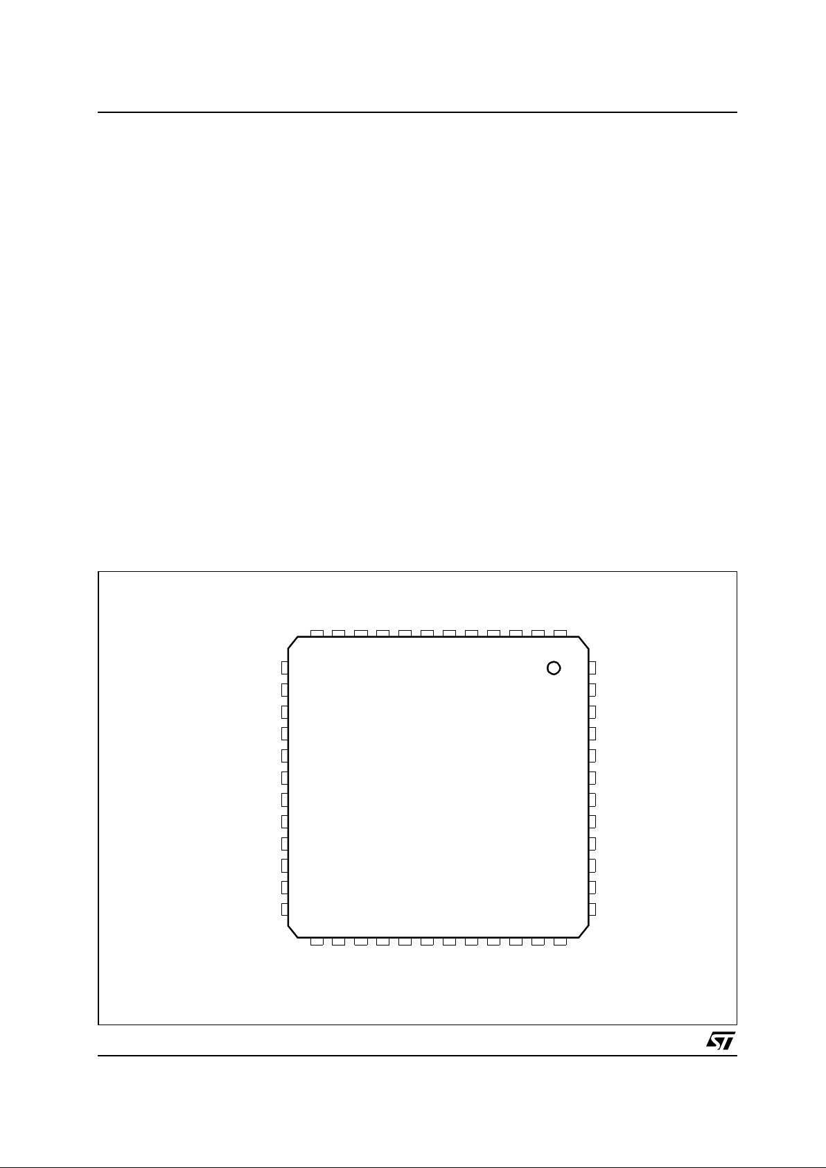
TQFP48
ORDERING NUMBER:
ST5481 TQF7
ST5481
PRODUCT PREVIEW
L.O.U.I.S - LOW COST USB ISDN SOLUTION
This is advance information on a new product now in development or undergoing evaluation. Details are subject to change without notic e.
Page 2
ST5481
2/18
1 - GENERAL PURPOSE
The ST5481 is a single chip ISDN -BRI with USB
Interface low cost controller. The purpose is a low
cost ISDN modem for applications like INTERNET
ACCES and FAX capabilities when the PC is ON
(full operating mode). The bonus is to offer an
easy and lowcost access to INTERNET at a rate
of 128kbits/sec. EASY access due to plug and
play features via USB bus and lowcost due to host
processing concept and remote powering via USB
bus features.
2 - MAIN FUNCTIONS
The device controls the S0 ISDN basic rate
access (ITU normalization I430) and manages the
B1, B2, D channels through the USB bus. B1, B2,
D channels data flow is regulated through FIFO
memories of respectively 32, 32, 16 bytes in each
direction. On D, B1, B2 channels, all upper
protocols than basic HDLC framing protocol
are host processed from upper-datalink protocol
(I440 normalization), network protocol up to
applications drivers. Link Activation, deactivation
protocols (I430) is managed by the device. But the
full handling of the command and indicate
primitives is done by the host processor
accessing to dedicated registers. Call setup
signalling frames through D channel are managed
by the host processor.
Internal regulators can be enabled to feed the
device (and external devices) via the GNDBUS,
VBUS USB powering lines. They convert the USB
5 volts to 3.3 volts.
The device respects the USB release 1.0 power
management recomm endat ions. When e ntered in
suspend mode on USB side the device drop into a
low power mode. An internal oscillator and a P LL
provide from an external 15.36MHz crystal a
48MHz clock for USB data rate recovering and
15.36MHz clock for S interface.
The device offers one operating mode called
CLOSED mode plus several test modes. In
CLOSED MODE the device presents the USB
interface, the S interface and 8 GPIO pins.
3 - PIN-OUT
Figure 1 : Pin-out Synoptic
1098765432112 11
48
47
46
45
44
43
42
41
40
39
38
37
27 28 29 30 31 32 33 34 35 3625 26
13
14
15
16
17
18
19
20
21
22
23
24
MODE3
MODE2
MODE1
MOD0
RPSM
GNDA
VREGA
VBUS
VREGD1
GNDBUS
DP
DM
DR_TEST5
FS_TEST4
CLK_TEST3
ID3_TEST2
ID2_TEST1
ID1_TEST14
ID0_TEST15
NRESET
VREGD2
GNDD2
CFG0/TEST0
GPIO7
GPIO6
GPIO5
GPIO4
GNDD1
GPIO3
GPIO2
GPIO1
GPIO0
XTALIN
XTALOUT
FLTPLL
LIP
LIN
IREF
LON
LOP
TEST13
TEST12
NCS_TEST11
SDI_TEST10
CFG1_TEST9
SDO_TEST8
SCK_TEST7
ST5481
DX_TEST6
Page 3
ST5481
3/18
3.1 - Pin List
Pin Name Type Function
1 DM I/O Negative USB differential data line
2 DP I/O Positive USB differential data line
3 GNDBUS I USB remote ground
4 VREGD1 I/O Digital input/ output regulated supply, is an input when RPSM is tied to a logic
zero value
5 VBUS I USB remote positive supply 5 volts.
6 VREGA I/O 3.3V input/ output analog regulated supply, is an input when RPSM is tied to a
logic zero value
7 GNDA I Analog groun d
8 RPSM I REMOTE POWER SUPPLY MODE: when tied to a logic zero value the device
is self powered
9 MODE0 I Static configuration pin. Used for working modes and test modes programming
10 MODE1 I Static configuration pin. Used for working modes and test modes programming
11 MODE2 I Static configuration pin. Used for working modes and test modes programming
12 MODE3 I Static configuration pin. Used for working modes and test modes programming
13 LIP In analog Receive AMI signal differential positive inputs from the S line
14 LIN In analog Receive AMI signal differential negative input from the S line
15 IREF In analog External current reference (connected to an external resistor)
16 LON Out analog Transmit AMI signal differential negative output to the S line
17 LOP Out analog Transmit AMI signal differential positive output to the S line
18 TEST13 Out analog Analog test pin: AOPTEST1
19 TEST12 Out analog Analog test pin: AOPTEST2
20 TEST11 I/O Test pin
21 TEST10 I/O Test pin
22 TEST9 I/O Test pin
23 TEST8 I/O Test pin
24 TEST7 I/O Test pin
25 TEST6 I/O Test pin
26 TEST5 I/O Test pin
27 TEST4 I/O Test pin
28 TEST3 I/O Test pin
29 ID3_TEST2 I/O Either ID product bit 2 for USB descriptor either test pin
30 ID2_TEST1 I/O Either ID product bit 3 for USB descriptor either test pin
31 ID1_TEST14 I Either ID product bit 1 for USB descriptor either test pin
32 ID0_TEST15 I Either ID product bit 0 for USB descriptor either test pin
33 NRESET I Initialisation input pin, zero active.
34 VREGD2 I Digital input supply, must be connected to VREGD1
Page 4
ST5481
4/18
3.2 - PLL
An internal oscillator provides a 15.36MHz clock for S interface from an external 15.36MHz crystal. From
this clock, the analog block PLL provides a 48MHz clock for USB data rate recovering.
35 GNDD2 I Digital ground
36 CFG0_TEST0 I/O CFG0 input for configuration when closed or open mode else test9
37 FLTPLL In analog Used to adjust the internal PLL filter
38 XTALOUT O Tied to 15.36MHz external crystal
39 XTALIN I Tied to 15.36MHz external crystal
40 GPIO0 I/O General purpose input-output pin 2mA
41 GPIO1 I/O General purpose input-output pin 2mA
42 GPIO2 I/O General purpose input-output pin 2mA
43 GPIO3 I/O General purpose input-output pin 2mA
44 GNDD1 I Digital ground
45 GPIO4 I/O General purpose input-output pin 4mA
46 GPIO5 I/O General purpose input-output pin 4mA
47 GPIO6 I/O General purpose input-output pin 4mA
48 GPIO7 I/O General purpose input-output pin 4mA
Pin Name Type Function
Page 5
ST5481
5/18
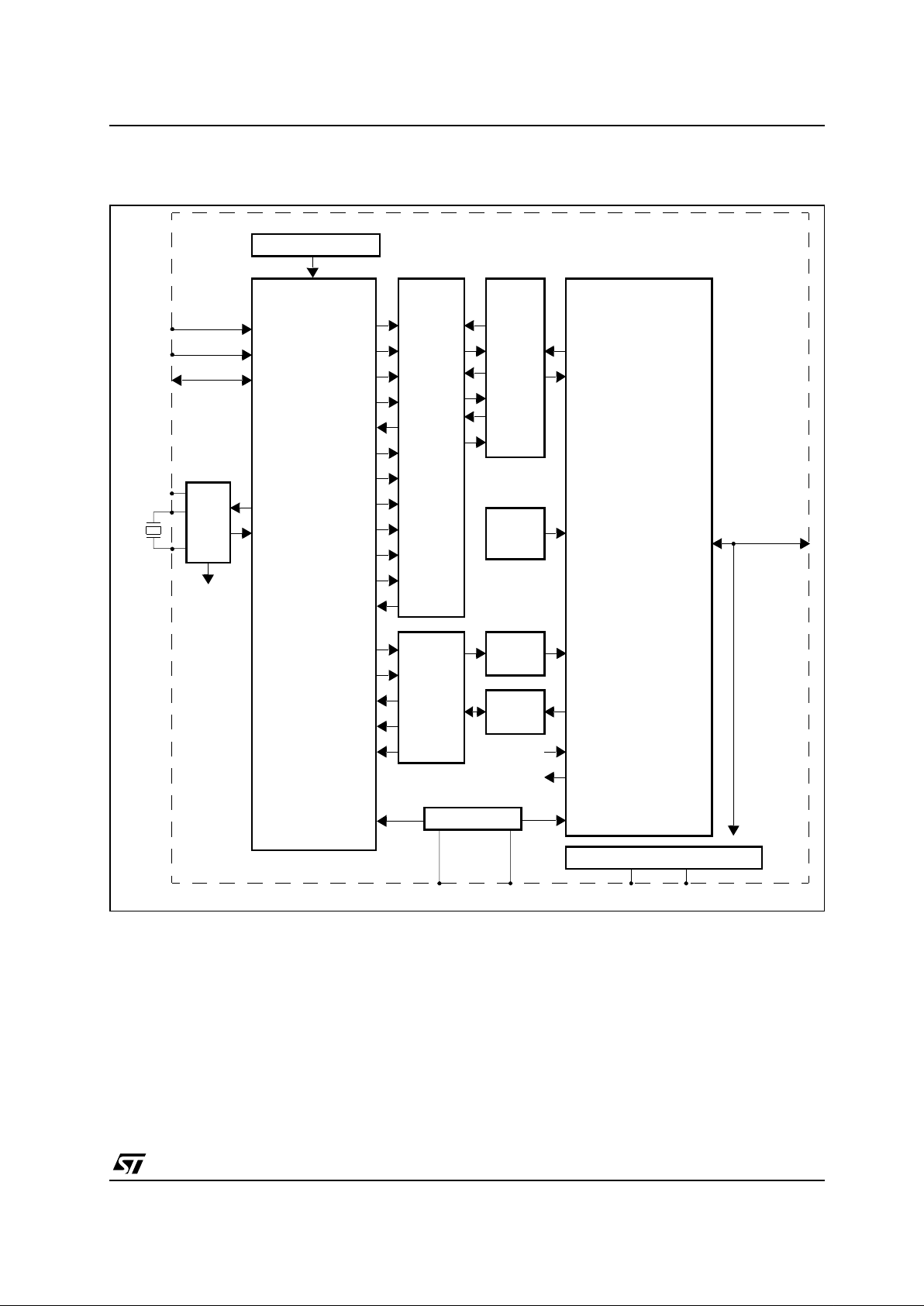
4 - SYNOPTIC
Figure 2 : Global Synoptic
I430
MACROCELL
MCLK
STOP_OSC
S0 interface
TXCK_O
IREF
VREF
NRESET
NINT
DEN
DREQ
NLSD
SDO
SDI
SCK
NCS
RXCK_O
TXFS_O
RXFS_O
TXDATA
RXDATA
B1_W
B2_W
D_W
TEST
VREF-GEN
CHANNEL
B1, B2, D
FIFOS
for
ROM
Descriptor
ACCESS
and
controller
Endpoint 1
Microwire
interface
controller
Endpoint 0
TEST interface
CK48
USB
MACROCELL
USB Driver
CK12
CONTROL_DATA_IN( 7-0)
CONTROL_DATA_O UT( 7-0)
TEST2-0
USB Bus
4
Power manag em ent and R EGU LATORS
8 power pinsRPSM
MODE(3-0)Test pins
15.36MHz
FLTPLL
PLL
15.36
48MHz
4
S0
CK48
isochonous
endpoints
256 bytes
FRAMING
Page 6
ST5481
6/18
5 - ISDN ACCESS
The device is directly connected to the ISDN line
at S0 interface point.
4 pins are dedicated to this access:
LIP, LIN: receive AMI differential signals inputs
connected to the appropriate transformer LOP,
LON: transmit AMI differential signals outputs
connected to the appropriate transformer.
The S interface access sub-function is clockfeeded by a 15.36MHz clock signal from the
on-chip oscillator.
I431 recommendation protocols are fully implemented.
The activation / deactivation command management is done by the device.
5.1 - ISDN S Interface Synoptic
See Figure 3.
6 - USB ACCESS
The device is directly connected to the USB bus.
4 pins are dedicated to this access:
DP, DM for data exchange. VBUS, GNDBUS as
power lines.
The data transfer rate is 12 MBits. The clock is
extracted from the differential lines DP, DM by a
digital PLL from a 48MHz internal clock. This
48MHz clock is created from the 15.36MHz clock.
The USB protocol is fully implemented following
the 1.0 USB specification.
6.1 - USB Normalization
This specification refers to USB normalization
documents:
– Universal Serial Bus Specification revision 1.0
– Universal Serial Bus Common Class S pecifica-
tion revision 1.0
– ST5481 belongs to the VENDOR SPECIFIC
DEVICE CLASS and to a vendor specific
subclass defined as ISDN MODEM DEVICE
SUBCLASS.
It presents ONE INTERFACE belonging to the
VENDOR SPECIFIC INTERFACE CLASS and a
vendor specific interface subclass defined as
ISDN SOFT MODEM INTERFACE SUBCLASS.
It satisfies to a vendor specific control protocol
called ISDN SOFT MODEM PROTOCOL.
Figure 3 : S-Interface Block Diagram
Line Signal
Rx
Slicers
RXNUMCONTROL
TXNUM
- Tx multiframe control
- D channel monitoring
- Loopbacks
- Frame construction
- AMI code generation
Detector
- C/I control
- Activation state machine
- Master clocks generation
- D & E channel processing
- Auto threshold controller
- Auto equalizer controller
- Digital PLL, line synchronization
- AMI decoder
- Frame synchronization & polarity check
- Signal ID
- Multiframe control.
Pre Filter &
equalizer
2x6 bits DA Cs
Line
Driver
Page 7

ST5481
7/18
7 - POWER MANAGEMENT
The device can be supplied by the USB bus
power lines VBUS (5 volts) and GNDBUS
(ground). This is enabled when RPSM (remote
power supply mode) is at logic one. Then on-chip
regulators bring 3.3 volts to internal analog and
digital blocks. When RPSM is high, a supply is
brought to external devices th rough pins G NDD1,
VREGD1, GNDD2, VREGD2, GNDA, VREGA.
The power budgeting is done by the host when
initializing the pipe:
The needed information (maximum power
consumption) is adjusted through pins CFG0,
CFG1 and as well as RPSM for “remote wake up
ability” information.
The following mechanism is used to do "a get
descript ion device" .
Figure 4 : Bus-Powered Mode (RPSM=1)
ST 5481
VBUS
RPSM
GNDBUS
VREGD1
GNDD1
VREGD2
GNDD2
VREGA
GNDA
From
To other
To other
8
5
3
4
44
34
35
6
7
digital
analog
device
device
USB bus
Figure 5 : Self Powered Mode (RPSM=0)
ST 5481
VBUS
RPSM
GNDBUS
VREGD1
GNDD1
VREGD2
GNDD2
VREGA
GNDA
From
8
5
3
4
44
34
35
6
7
From 3.3V
externally
regulated
supplies
USB bus
Page 8

ST5481
8/18
The host gets back the configuration of the device
either a low power device, either a high power
device (max power parameter higher than
100mA). Being a high power device allows to set
on a wake up ability because looking for a line
signal detection consume more than 500uA
allowed for a low power device when in a suspend
state.
To adjust the maximum power consumption
parameter into the configuration descriptor, the
logical values present on pins CFG0, CFG1,
RPSM are used (see Table 1).
At power on, the digital regulator is im mediately
ON and after 100µs the analog regulator is
authorized to feed the internal oscillator.
– Initialization and clocks management.
– A HARDWA RE PIN RESET is done through pin
NRESET (active low).
– A delay of 4.5ms is introduced before distribut-
ing the clocks to the inte rn al fun ctions.
– A USB HARDWARE RESET is done through
DP, DM pins. This reset affects the USB interface, resetting the USB core state machines. It
does not affect the application (S interface, registers, fi fo s).
A USB SOFTWARE RESET is done through USB
bmRequest SET_DEFAULT. It brings the S
interface, application registers, application state
machines and fifos pointers to default state.
When the device goes out of S USPEND_CLOCK
state, a delay of 4.5ms is introduced before
distributing the clocks to the internal functions.
When the device enters into a suspend mode due
to inact ivity on US B bus, th e oscillat or is stopp ed
in order to save power except if FCONF(3) is
equal to 1.
Table 1 : Maximum Power Current and Wake up Ability Coding
Max Power
Current
High/Low
Power
Wake Up
Ability
CFG1 CFG0 RPSM
Bm Attributes
ROM add 27
Max Power
ROM add 28
100 mA LO NO 0 0 1 80 32
150 mA HI NO 0 1 1 80 96
150 mA HI YES 1 0 1 A0 96
250 mA HI YES 1 1 1 A0 F9
100 mA LO NO 0 0 0 C0 32
150 mA HI NO 0 1 0 C0 96
150 mA HI YES 1 0 0 E0 96
250 mA HI YES 1 1 0 E0 F9
Page 9

ST5481
9/18
8 - DEVICE STATES
The device complies with USB rev 1.1 power
management requiremen ts.
It complies with I430 power management
requirements.
Due to inactivity on the USB bus for mo re than 3
ms, the device may enter into the SUSPEND
mode even if Reset signalling is not done yet.
The ST5481 recovers activity within the 15ms of
the resume signalling issued by the host or hub.
If wake up is enabled and occurs, the ST5481
recovers activity within the 15 ms when it initiates
the resume (K state) and about the same time the
host or hub initiates a Reset (SEO for 10 ms).
Wake up ability concerns wake up of the USB bus
(resume event when the bus is in a suspend state)
from the S line through a line signal detection
done by the S interface.
Interface S states and relationship with Device
versus USB States.
M1: QUIET mode (initial mode if CFG1 = 0).
It means that S interface cannot be activated
neither by the host nor by a dete ction of signal on
line. This signal detection is disabled. The 15MHz
oscillator is not addressed to MACRO-S
M2: ACTIVE Mode.
When the device is in S6,S7,S8,S9 states from
USB point of vi ew, the S interface may be in t his
state, then it can be deactivated by a PDN
primitive (from host) or a hardware power down
which is generate d by a suspend event on USB
bus
M3: INACTIVE Mode (initial mode if CFG1 = 1).
The line signal detection is ena bled. Then it can
be activated (go t o st ate A CTI VE) by a line signal
detection.
When USB is suspended, The S interface will
really be in the active mode once a resume
signalling has been done on USB bus after the
NLSD signal became active.
When USB is configured, a transition from this
mode to ACTIVE mode is obtained with a PUP
primitive (from host).
Figure 6 : S Interface States - CFG1=0
PON RESET /
USB REQUEST/
PIN RESET
M3
M2
STT(5)=0
STT(5)=1
PDN or PDWN=1
PUP or NLSD=0
STT(5)=1
M1 OFF
S LINE ACTIVATION
ACTIVE
INACTIVE S LINE ACTIVATION
POSSIBLE
NOT POSSIBLE
Page 10

ST5481
10/18
If Pin CFG1 is 1, when reset (PON,USB,PIN) is active the initial state is INACTIVE.
9 - ENDPOINTS CONFIGURATION AND DEDICATION
These endpoints are org anized as one interface
(interface 0), one configuration (configuration 1).
The interface being composed of four alternate
settings. Hereafter in the document RX data
direction is from S line to PC and is considered as
IN by USB protocol.
The endpoints are:
– 4 isochronous endpoints for B1 and B2 channels
(fifo 32 bytes in each direction)
• EP3 input endpoint for B1 channel IN(RX) on S
line
- associated to IN(RX) fifo 32 bytes
• EP2 output endpoint for B1 channel OUT(TX)
on S line
- associated to OUT(TX) fifo 32 bytes
• EP5 input endpoint for B2 channel IN(RX) on S
line
- associated to IN(RX) fifo 32 bytes
• EP4 output endpoint for B2 channel OUT(TX)
on S line
- associated to OUT(TX) fifo 32 bytes
– 2 isochronous endpoin ts for D channels (fifo 16
bytes in each direction)
• EP7 input endpoint for D channel IN(RX) on S
line
- associated to IN(RX) fifo 16 bytes
• EP6 output endpoint for D channel OUT(TX) on
S line
- associated to OUT(TX) fifo 16 bytes
– 1 control endpoint means managem ent of USB
standards, Communication Device Class (CDC)
standards (unused), and vendor reques ts (S interface application dedicated):
• EP0
- internal configuration and control registers
- D, B1, B2 channels transmit commands
- CI primitives to be transmitted
– 1 interrupt endpoin t used for vendor interrupts
• EP1
- channels reception or transmission indications
- CI primitives in receive direction
- D, B1, B2 channel reception indications
- S line status
- GPIO input changes
The alternate settings are:
• Alternate setting 0: EP0, EP1.
- initialisation configuration
•
Alternate setting 1: EP0, EP1, EP2, EP3, P6, EP7
- connection 64Kbits through B1 channel
•
Alternate se ttin g 2: EP0 , EP1 , EP 4, EP 5, EP 6, E P7
- connection 64Kbi ts through B2 chan nel
• Alternate setting 3: EP0, EP1, EP2, EP3, EP4,
EP5, EP6, EP 7
- connection 128Kbps (144Kbits/sec) through
B1 + B2 + (data into D) channels
Figure 7 : S Interface States - CFG1=1
OFF
PON RESET /
USB REQUEST/
PIN RESET
M3
M2
STT(5)=0
STT(5)=1
PDN or PDWN=1
PUP or NLSD=0
STT(5)=1
M1 OFF
S LINE ACTIVATION
NOT POSSIBLE
ACTIVE
INACTIVE S LINE ACTIVATION
POSSIBLE
Page 11

ST5481
11/18
USB Descriptors
During the USB request GET DESCRIPTOR, the device returns these v alues from an internal 25 6 byte
ROM.
Notes 1. Th i s word represen ts the ha rdware -softwar e associ ation. T he value i s program m able through 4 of the 16 bits . the lower bits values
are define d by pins ID3 to ID 0.
2. This word represents the silicon hardwar e. The lower 8 -bit value is define d at metal layer . The other 8 bits are written into the RO M
at diffusio n l ayer.
Note 1. Theses words are defin ed by a transcodi ng of the pins CFG0, CFG1, RPSM : see power management section for coding of these
pins.
Table 2 : Device Descriptor
ROM addr Offset Field Size Value Description
08 0 bLengh 1 12h Size of this descriptor in bytes
09 1 bDescriptorType 1 01h Device Descriptor type
0A 2 bcdUSB 2 0101h USB spec release number 1.1
0C 4 bDeviceClass 1 FFh Vendor Specific Class code
0D 5 bDeviceSubClass 1 01h Vendor specific ISDN MODEM subclass
0E 6 bDeviceProtocol 1 01h Vendor specific ISDN SOFT MODEM control protocol
0F 7 bMaxPacketSize0 1 08h Max packet size for EP0
10 8 idVendor 2 0483h ST id vendor
12 10 idProduct 2 481xh
Application id product
1
14 12 bcdDevice 2 01xxh
Device release
2
16 14 iManufacturer 1 00h No specific manufacturer registred
17 15 iProduct 1 01h product id String descriptor index 1
18 16 iSerialNumber 1 00h No specific serial number registred
19 17 bNumConfigurations 1 01h Number of possible configurations
Table 3 : Interface 0 as 0 Descriptor
ROM addr Offset Field Size Value Description
20 0 bLengh 1 09h Size of this descriptor in bytes
21 1 bDescriptorType 1 02h Configuration Descriptor type
22 2 wTotalLengh 2 00CFh Total length of data byte returned for this configuration
24 4 bNumInterface 1 01h number of interfaces supported by this configuration
25 5 bConfigurationValue 1 01h value used to select this conf.
26 6 iConfiguration 1 00h No specific string descriptor for this configuration
27 7 bmAttributes 1
XXh
Self powered and remote wake-up abilities
programmable
1
28 8 MaxPower 1 XXh
max consumption programmable
1
Page 12

ST5481
12/18
10 - ELECTRICAL SPECIFICATIONS
Unless otherwise stated, electrical characteristics are specified over the operating range.
Typical values are given for VBUS = +5V, VregA = 3.3V, VregD1 = VregD2 = 3.3V, Tamb = 25°C
10.1 - Absolute Maximum Rating
Notes GNDA = GNDD1 = GNDD2 = GNDBUS = 0V
Warning : Operation beyond these limits may result in permanent damage to the device. Normal operation is not guaranteed at these
extremes.
1. In Remote Power Supply Mode (RPSM=0)
2. For the ISDN S side access “LOP,LON,LIP , LIN” pins the voltage level can temporary exceed the maximum rating due to the phone
line conditions. To prevent any damage to the circuit, an external protection circuit must be implemented according to the application
schematics.
10.2 - Nominal DC Characteristics
(Ta = 0 to 70°C unless otherwise specified)
Note 1. VREGD2 is al ways an analog powe r i nput, to be connected to VREGD1
Table 4 : Absolute maximum ratings
Symbol Parameter Value Unit
VBUS
5V Power Supply Voltage
5.5V V
VREGD1
3.3V Power Supply Voltage
1
-0.3V to 3.6V V
VREGD2
3.3V Power Supply Voltage
1
-0.3V to 3.6V V
VREGA
3.3V Power Supply Voltage
1
-0.3V to 3.6V V
V
IA
Analog Input Voltage
2
-0.3 to V
REGA
+ 0.3V V
V
ID
Digital Input Voltage -0.3 to V
REGDX
+ 0.3V V
V
ID
Digital Input Voltage on RPSM -0.5 to VBUS + 0.3V V
T
oper
Operating Temperature 0, +70 °C
T
stg
Storage Temperature -55, +125 °C °C
Table 5 : Nominal DC characteristics
Symbol Parameter Minimum Typical Maximum Unit
VBUS Supply voltage 4 5 5.25 V
Ivdd Supply Current (RPSM=1) TBD TBD mA
Ivdds Supply Current in Suspended Mode (RPSM=1) TBD mA
VREGA Analog regulated OUTPUT power supply (RPSM=1)
Analog regulated INPUT power supply (RPSM=0)
3.3-5% 3.3 3.3+5% V
VREGD1 Digital regulated OUTPUT power supply (RPSM=1)
Digital regulated INPUT power supply (RPSM=0)
3.3-5% 3.3 3.3+5% V
VREGD2
Digital regulated INPUT power supply
1
3.3-5% 3.3 3.3+5% V
I
VregA
Analog regulated OUTPUT current (RPSM=1)
Analog regulated INPUT current (RPSM=0)
TBD 40 mA
I
VregD1
Digital regulated OUTPUT current (RPSM=1)
Digital regulated INPUT current (RPSM=0) TBD
40 mA
I
VregD2
Digital regulated INPUT current
1
TBD mA
P
DLP
Low Power mode (Suspended mode) TBD mW
P
D
Operating Power TBD mW
Page 13

ST5481
13/18
A 2.2µF decoupling polarized capacitor (tantal or chemical) is necessary as between VREGA and GNDA.
A 1µF decoupling polarized capacitor (tantal or chemical) is necessary as between VREGD1 and
GNDD1.
A 1µF decoupling polarized capacitor (tantal or chemical) is necessary as between VREGD2 and
GNDD2.
Note A 10ms time constant will be used (ex: 470 nF, 20Ω) to genera te an adequate pulse on NRESET pin.
Table 6 : Digital Pins (except GPIO4 to GPIO7,XTALin, XTALout, RPSM, NRESET)
Symbol Parameter Minimum Typical Maximum Unit
V
IL
Low level input voltage 0.2V
RegD1
V
V
IH
High level input voltage 0.8V
RegD1
V
V
OL
Low level input voltage (ILoad = 2mA) 0.4 V
V
OH
High Level Output Voltage (Iload = -2mA) 0.85V
RegD1
V
I
LEAK
Input Leakage Current 1 uA
I
OL
Low level input Current (0<Vol<Volmax) -2 mA
I
OH
High Level Output Current (Vohmin<Vof<VregD1) 2 mA
V
HYST
Schmitt Trigger Hysteresis 0.8 V
C
IN
Input Capacitance 3 pF
Table 7 : GPIO4, GPIO5, GPIO6, GPIO7.
Symbol Parameter Minimum Typical Maximum Unit
V
IL
Low level input voltage 0.2V
RegD1
V
V
IH
High level input voltage 0.8V
RegD1
V
V
OL
Low level input voltage (Iload = 2mA) 0.4 V
V
OH
High Level Output Voltage (Iload = -2mA) 0.85V
RegD1
V
I
LEAK
Input Leakage Curren t 1 uA
I
OL
Low level input Current (0<Vol<Volmax) -4 mA
I
OH
High Level Output Current (Vohmin<Vof<VregD1) 4 mA
V
HYST
Schmitt Trigger Hysteresis 0.8 V
C
IN
Input Capacitanc e 3 pF
Table 8 : RPSM, NRESET. (5 volt inputs compatible)
Symbol Parameter Minimum Typical Maximum Unit
V
IL
Low level input voltage 0.3V
BUS
V
V
IH
High level input voltage 0.7V
BUS
V
V
HYST
Schmitt Trigger Hysteresis 1 1.3 V
Page 14

ST5481
14/18
Table 9 : Crystal Oscillator (XTALin, XTALout)
Note Manufac turer exam pl e: Ref MMD A2 0BA1- 15. 36M Hz
10.3 - Universal Serial Bus Interface
See Chapter 7 of USB rev1.0 for complete Electrical Specification
See Chapter 7 of USB rev1.0 for complete Electrical Specification.
Note Excludes external resistor. In order to comply with USB Specification 1.0, external series resistors of 27Ω ±1% each on DP and DM
are recommended.
AC Characteristics (DP, DM)
See Chapter 7.3.2 of USB rev1.0 for complete Electrical Specification.
Symbol Parameter Minimum Typical Maximum Unit
V
IL
Low level input voltage 0.2V
RegD1
V
V
IH
High level input voltage 0.8V
RegD1
V
I
L
Low level input Current -TBD uA
I
H
High Level Output Current TBD uA
ESR Electrical Serial Resistor 25 Ω
CO Shunt capacitance 7 pF
Table 10 : 48MHz Internal PLL
Symbol Parameter Minimum Typical Ma ximum Unit
JiTTER Jitter peak-peak Magnitude 0.35 5 ns
Lock Time High level input voltage 60 100 us
Table 11 : USB Nominal DC Characteristics (DP, DM)
Symbol Parameter Minimum Typical Maximum Unit
V
DI
Differential Input Sensitivity [(DP)-(DM)] 0.2 V
V
CM
Differential Common Mode Range 0.8 2.5 V
V
SE
Single Ended Receiver Threshold 0.8 2 V
V
OH
High Level output Static voltage (RL of 15KΩ to GND) 2.5 3.6 V
V
OL
Low level input Static voltage (RL of 1.5KΩ to 3.6V) 0.3 V
I
LO
Hi-Z State Data Line Leakage Current (0v <Vin <3,3V) ± 10 uA
C
in
Transceiver Capacitance (Pin to GND) 20 pF
R
D
Driver Output Resistance (steady state drive) TBD TBD kΩ
Page 15

ST5481
15/18
10.4 - Line Side Isdn S Interface
Note UIT-TI430, ETSI 30 0012, ANSI T1.605 sta ndards com pl i ance.
11 - APPLICATION SYNOPTIC
11.1 - Global Environme nt
Table 12 : ISDN Interface Electrical Characteristics: R
IREF
= 120kΩ
Symbol Parameter Minimum Typical Maximum Unit
I
TX
TX Line Driver current with 70Ω between LOP / LON
[ 70 (total)= 50 (load) + 2 x 7 (serial) + 2 x 3 (serial) ]
14.25 15 15.75 mA
I
TX
TX Line Driver current with 420Ω between LOP / LON
[ 420 (total)= 400 (load) + 2 x 7 (serial) + 2 x 3 (serial) ]
3mA
I
TX
TX Line Driver current with 25.6Ω between LOP / LON
[ 25.6(total)= 5.6 (load) + 2 x 7 (serial) + 2 x 3 (serial) ]
26 mA
Z
OTX
Transmit Output impedance during pulse.
( 20Ω is obtained as total min value with serial resistors:
[ 20(total)= Z
OTX
+ 7(serial) + 7(serial) ])
6kΩ
Z
TX
Impedance when inactive, between LOP / LON 2.5 kΩ
Z
INRX
Receive Input impedance between LIP / LIN 2.5 kΩ
Figure 8 : Synoptic
ISDN USB dongle
RJ45
USB
ST5481
NT1
Usb cable
S interface
Plug B
Page 16

ST5481
16/18
11.2 - Application Schematic
Figure 9 : Schematic
U3
DALC208SC6
3635343332313029282726
25
dx/test6
dr/test5
fs/test4
clk/test3
id2/test2
id3/test1
id1/test14
id0/test15
nreset
Vregd2
Gndd2
Cfg0/test0
13 14 15 16 17 18 19 20 21 22 23 24
gpio7
lip
lin
iref
lon
lop
test12
test13
ncs/test11
sdi/test10
cfg1/test9
sd0/test8
sck/test7
48 47 46 45 44 43 42 41 40 39 38 37
123456789
101112 mode3
mode2
mode1
mode0
rpsm
GndA
VregA
Vbus
Vregd1
Gndbus
DP
DM
U1
ST5481
gpio6
gpio5
gpio4
Gndd1
gpio3
gpio2
gpio1
gpio0
xtalin
xtalout
fltpll
C1
47pF
R7
C2
33pF
C3
33pF
Y1 15.36MHz
C4
100nF
R2
220KΩ
VCC
R1
D1
GND.D1/D2GNDA
C8
100nF
C10
2.2µF
6 5
U2
USBUF01W6
R19
123
4
161514
13
2:1
2fold-Choke
2x5mH
T60407
2:1
2fold-Choke
2x5mH
567
8
121110
9
T1
R20
1234567
8
RJ45
R21
D2
LED
LED
510Ω
510Ω
1KΩ
C9
4.7µF
R15
1MΩ
+
4.7Ω
4.7Ω
R23
10KΩ 1%
C11
100nF
R22
10KΩ 1%
L526X010
321
I/02
ref2
I/01
456
I/03
ref1
I/04
12
D3 SMLTV3/3
VCC
+
R17
120KΩ
R18
4.7MΩ
C7
10µF
+
4
D+out VCC D- out
1 2 3
D+in GND D-in
VCC
R16
0Ω
D+
D-
L1
4.7µH
123
4
USB-B
56
J1
J2
Page 17

ST5481
17/18
TQFP48 PACKAGE MECHANICAL DAT A
Figure 10 : 48 Pins - Full Plastic
Dimension
Millimeter Inch
Minimum Typical Ma ximum Minimum Typical Maximum
A 1.60 0.063
A1 0 .05 0.15 0.002 0.006
A2 1 .35 1.40 1.45 0.053 0.055 0.057
B 0 .17 0.22 0.27 0.007 0.009 0.011
C 0.09 0.20 0.004 0.008
D 9.00 0.354
D1 7 .00 0.276
D3 5 .50 0.216
e 0.50 0.0197
E 9.00 0.354
E1 7.00 0.276
E3 5.50 0.216
L 0.45 0.60 0.75 0.018 0.024 0.030
L1 1 .00 0.039
K 0° (minimum), 7° (maximum)
48 37
D3
e
13 24
1
12
25
36
c
A1
A2
A
D1
D
E3
E1
E
L
K
L1
0,25 mm
.010 inch
GAGE PLANE
0,10 mm
.004 inch
SEATING PLANE
B
Page 18

18/18
Information furnished is bel ieved to be accurate and reliable. However, STMicroe lectronics assumes no responsibility for the
consequences of use of such information nor for any infringement of patents or other rights of third parties which may result from
its use. No li cense is granted by i mp lication or otherwise under any patent or patent rights of STMicroelectronics. Specifications
mentioned in this publication ar e subject to change without notice. This publication supersedes and replaces all information
previously supplied. S TMicroelectronics products are not authorized for use as critica l components in life suppo rt devices or
systems without express written approval of STMicroelectronics.
The ST logo is a registered trademark of STMicroelectronics
© 2000 STMicroelectronics - All Rights Reserved
STMicroele ct ronics GROUP OF C OM P A NI E S
Australi a - Brazil - Chi na - Finlan d - F rance - Germ any - Hong Kong - India - Ital y - Japan - Ma l aysia - Malta - Morocco
Singapo re - Spain - Sweden - Swit zerland - United Kingdom - U.S. A.
http://www.st.com
ST5481.REF
 Loading...