

Page 1
®
LOG100
Precision
LOGARITHMIC AND LOG RATIO AMPLIFIER
FEATURES
● ACCURACY
0.37% FSO max Total Error
Over 5 Decades
● LINEARITY
0.1% max Log Conformity
Over 5 Decades
● EASY TO USE
Pin-selectable Gains
Internal Laser-trimmed Resistors
● WIDE INPUT DYNAMIC RANGE
6 Decades, 1nA to 1mA
● HERMETIC CERAMIC DIP
DESCRIPTION
The LOG100 uses advanced integrated circuit technologies to achieve high accuracy, ease of use, low
cost, and small size. It is the logical choice for your
logarithmic-type computations. The amplifier has guaranteed maximum error specifications over the full sixdecade input range (1nA to 1mA) and for all possible
combinations of I
that involved error computations are not necessary.
The circuit uses a specially designed compatible thinfilm monolithic integrated circuit which contains amplifiers, logging transistors, and low drift thin-film
and I2. Total error is guaranteed so
1
APPLICATIONS
● LOG, LOG RATIO AND ANTILOG
COMPUTATIONS
● ABSORBANCE MEASUREMENTS
● DATA COMPRESSION
● OPTICAL DENSITY MEASUREMENTS
● DATA LINEARIZATION
● CURRENT AND VOLTAGE INPUTS
resistors. The resistors are laser-trimmed for maximum precision. FET input transistors are used for the
amplifiers whose low bias currents (1pA typical) permit signal currents as low as 1nA while maintaining
guaranteed total errors of 0.37% FSO maximum.
Because scaling resistors are self-contained, scale
factors of 1V, 3V or 5V per decade are obtained
simply by pin selections. No other resistors are required for log ratio applications. The LOG100 will
meet its guaranteed accuracy with no user trimming.
Provisions are made for simple adjustments of scale
factor, offset voltage, and bias current if enhanced
performance is desired.
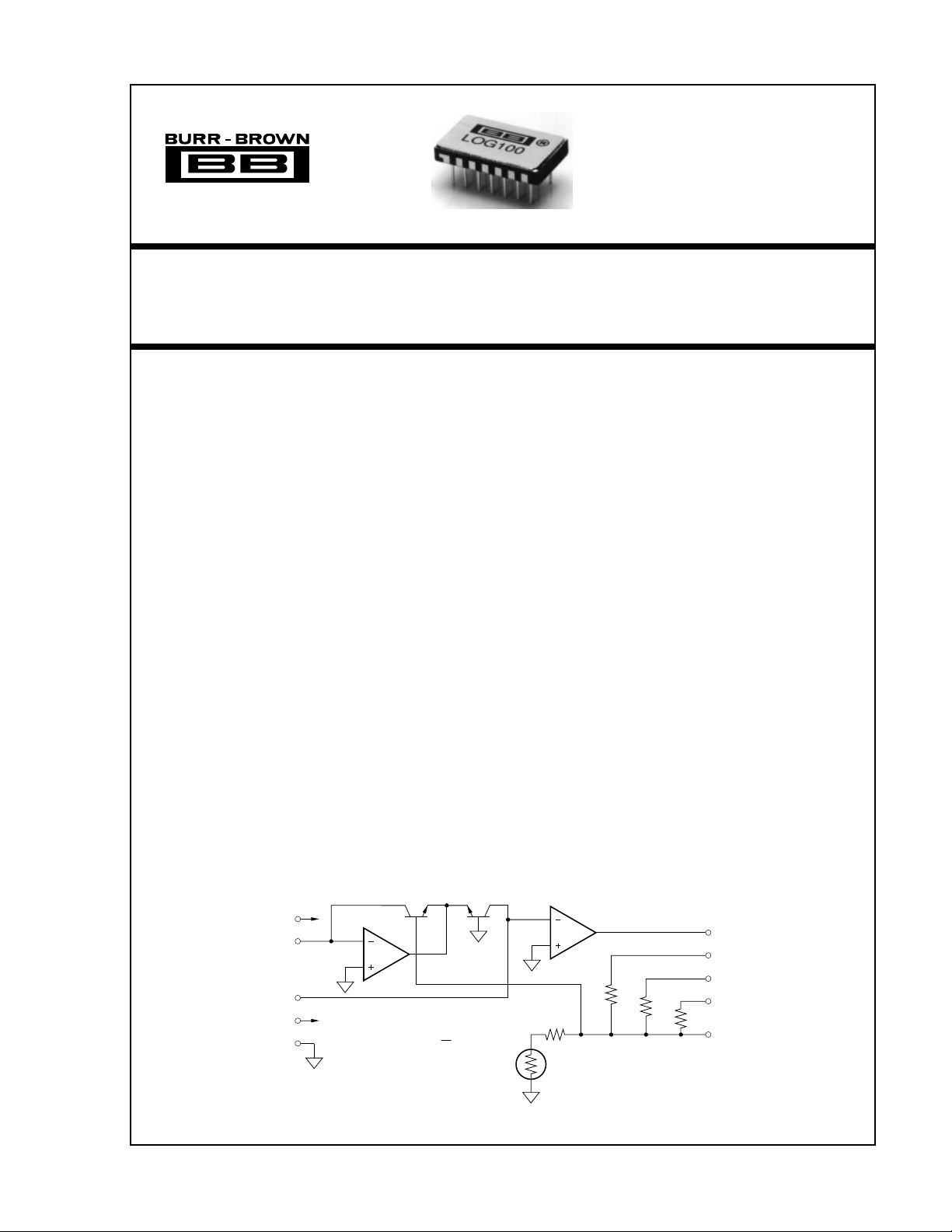
Q
9
–V
CC
1
I
1
14
I
2
6
+V
CC
10
Com
International Airport Industrial Park • Mailing Address: PO Box 11400 • Tucson, AZ 85734 • Street Address: 6730 S. Tucson Blvd. • Tucson, AZ 85706
Tel: (520) 746-1111 • Twx: 910-952-1111 • Cable: BBRCORP • Telex: 066-6491 • FAX: (520) 889-1510 • Immediate Product Info: (800) 548-6132
© 1981 Burr-Brown Corporation PDS-437E Printed in U.S.A. January, 1995
1
A
1
V
= K LOG
OUT
Q
2
A
2
7.5kΩ
24kΩ
I
1
I
2
PDS-437E
270Ω
220Ω
Resistor values nominal only;
laser-trimmed for precision gain.
39kΩ
7
3
4
5
2
V
OUT
K = 1
K = 3
K = 5
Scale
Factor
Trim
Page 2

SPECIFICATIONS
ELECTRICAL
TA = +25°C and ±VCC = ±15V, after 15 minute warm-up, unless otherwise specified.
LOG100JP
PARAMETER CONDITIONS MIN TYP MAX UNITS
TRANSFER FUNCTION V
Log Conformity Error
Initial 1nA to 100µA (5 decades) 0.04 0.1 %
(1)
Either I1 or I
2
1nA to 1mA (6 decades) 0.15 0.25 %
Over Temperature 1nA to 100µA (5 decades) 0.002 %/°C
K Range
(2)
1nA to 1mA (6 decades) 0.001 %/°C
Accuracy 0.3 %
Temperature Coefficient 0.03 %/°C
ACCURACY
Total Error
Initial I
vs Temperature I
vs Supply I
INPUT CHARACTERISTICS (of Amplifiers A
Offset Voltage
(3)
K = 1,
and A2)
1
(4)
Current Input Operation
, I2 = 1mA ±55 mV
1
I
, I2 = 100µA ±30 mV
1
I
, I2 = 10µA ±25 mV
1
I
, I2 = 1µA ±20 mV
1
I
, I2 = 100nA ±25 mV
1
I
, I2 = 10nA ±30 mV
1
I
, I2 = 1nA ±37 mV
1
, I2 = 1mA ±0.20 mV/°C
1
I
, I2 = 100µA ±0.37 mV/°C
1
I
, I2 = 10µA ±0.28 mV/°C
1
I
, I2 = 1µA ±0.033 mV/°C
1
I
, I2 = 100nA ±0.28 mV/° C
1
I
, I2 = 10nA ±0.51 mV/°C
1
I
, I2 = 1nA ±1.26 mV/°C
1
, I2 = 1mA ±4.3 mV/V
1
I
, I2 = 100µA ±1.5 mV/V
1
I
, I2 = 10µA ±0.37 mV/V
1
I
, I2 = 1µA ±0.11 mV/V
1
I
, I2 = 100nA ±0.61 mV/V
1
I
, I2 = 10nA ±0.91 mV/V
1
I
, I2 = 1nA ±2.6 mV/V
1
Initial ±0.7 ±5mV
vs Temperature ±80 µV/°C
Bias Current
Initial 15
vs Temperature Doubles Every 10 °C
Voltage Noise 10Hz to 10kHz, RTI 3 µVrms
Current Noise 10Hz to 10kHz, RTI 0.5 pArms
AC PERFORMANCE
3dB Response
1nA C
1µAC
10µAC
1mA C
Step Response
(6)
, I2 = 10µA
(6)
= 4500pF 0.11 kHz
C
= 150pF 38 kHz
C
= 150pF 27 kHz
C
= 50pF 45 kHz
C
Increasing CC = 150pF
1µA to 1mA 11 µs
100nA to 1µA 7 µs
10nA to 100nA 110 µs
Decreasing C
1mA to 1µA 45 µs
= 150pF
C
1µA to 100nA 20 µs
100nA to 10nA 550 µs
OUTPUT CHARACTERISTICS
Full Scale Output (FSO) ±10 V
Rated Output
Voltage I
Current V
Current Limit
= ±5mA ±10 V
OUT
= ±10V ±5mA
OUT
Positive 12.5 mA
Negative 15 mA
Impedance 0.05 Ω
= K Log (I1/I2)
OUT
1, 3, 5 V/decade
(5)
pA
®
LOG100
2
Page 3
®
SPECIFICATIONS (CONT)
ELECTRICAL
TA = +25°C and ±VCC = ±15V, after 15 minute warm-up, unless otherwise specified.
LOG100JP
PARAMETER CONDITIONS MIN TYP MAX UNITS
POWER SUPPLY REQUIREMENTS
Rated Voltage ±15 VDC
Operating Range Derated Performance ±12 ±18 VDC
Quiescent Current ±7 ±9mA
AMBIENT TEMPERATURE RANGE
Specification 0 +70 °C
Operating Range Derated Performance –25 +85 °C
Storage –40 +85 °C
NOTES: (1) Log Conformity Error is the peak deviation from the best-fit straight line of the V
output. (2) May be trimmed to other values. See Applications section. (3) The worst-case Total Error for any ratio of I
I
and I2 are considered separately. (4) Total Error at other values of K is K times Total Error for K = 1. (5) Guaranteed by design. Not directly measurable due to
1
amplifier’s committed configuration. (6) 3dB and transient response are a function of both the compensation capacitor and the level of input current. See Typical
Performance Curves.
ABSOLUTE MAXIMUM RATINGS
Supply ................................................................................................ ±18V
Internal Power Dissipation .............................................................. 600mV
Input Current..................................................................................... 10mA
Input Voltage Range .......................................................................... ±18V
Storage Temperature Range ........................................... –40°C to +85°C
Lead Temperature (soldering, 10s) ............................................... +300°C
Output Short-circuit Duration .................................. Continuous to ground
Junction Temperature...................................................................... 175° C
PIN CONFIGURATION
SCALE FACTOR PIN CONNECTIONS
K, V/DECADE CONNECTIONS
5 5 to 7
3 4 to 7
1.9 4 and 5 to 7
1 3 to 7
0.85 3 and 5 to 7
0.77 3 and 4 to 7
0.68 3 and 4 and 5 to 7
FREQUENCY COMPENSATION
vs Log IIN curve expressed as a percent of peak-to-peak full scale
OUT
Bottom View
I
Common
2
–V
Input
NC
NC
NC
CC
NC
14
13
12
11
10
9
8
NC = No Connection
is the largest of the two errors when
1/I2
1
I1 Input
2
Scale Factor Trim
3
K = 1
4
K = 3
5
K = 5
6
+V
CC
7
Output
ELECTROSTATIC
DISCHARGE SENSITIVITY
Any integral circuit can be damaged by ESD. Burr-Brown
9
1
LOG100
14
6
543
7
10
recommends that all integrated circuits be handled with
appropriate precautions. Failure to observe proper handling
and installation procedures can cause damage.
ESD damage can range from subtle performance degradation to complete device failure. Precision integrated circuits
may be more susceptible to damage because very small
C
C
parametric changes could cause the device not to meet
published specifications.
ORDERING INFORMATION
SPECIFIED
TEMPERATURE
MODEL PACKAGE RANGE
LOG100JP 14-Pin Hermetic Ceramic DIP 0°C to +70°C
PACKAGE INFORMATION
MODEL PACKAGE NUMBER
LOG100JP 14-Pin Hermetic Ceramic DIP 148
NOTES: (1) For detailed drawing and dimension table, please see end of data
sheet, or Appendix D of Burr-Brown IC Data Book. (2) During 1994, the package
was changed from plastic to hermetic ceramic. Pinout, model number, and
specifications remained unchanged. The metal lid of the new package is
internally connected to common, pin 10.
3
PACKAGE DRAWING
(2)
LOG100
(1)
Page 4

TYPICAL PERFORMANCE CURVES
TA = +25°C, VCC = ±15VDC, unless otherwise noted.
NORMALIZED TRANSFER FUNCTION
3 (K)
V
= K Log
2 (K)
OUT
1 (K)
0 (K)
–1 (K)
–2 (K)
Normalized Output Voltage (V)
–3 (K)
0.01 1 100
0.001
TOTAL ERROR vs INPUT CURRENT
±75
±50
±25
Maximum Total Error (mV)
0
1nA
100nA 10µA 1mA
Input Current ( I
I
1
I
2
0.1 10 1000
I
or I2)
1
1
I
2
Current Ratio,
ONE CYCLE OF NORMALIZED TRANSFER FUNCTION
1 (K)
0.9 (K)
0.8 (K)
0.7 (K)
0.6 (K)
0.5 (K)
0.4 (K)
0.3 (K)
0.2 (K)
Normalized Output Voltage (V)
0.1 (K)
0
261103
TRIMMED OUTPUT ERROR vs INPUT CURRENT
60
Gain Error and
50
Offset Error Trimmed
40
to Zero
30
1
I
20
10
0
Trimmed Output Error (mV)
–10
–20
1nA
100nA 10µA 1mA
Input Current (I
Current Ratio,
or I2)
1
48
I
1
I
2
–60
–50
–40
–30
2
I
–20
–10
0
10
20
MINIMUM VALUE OF COMPENSATION CAPACITOR
1M
Select CC for
100k
(pF)
C
min and I2 max
I
1
= 10nA
I
1
10k
= 100nA
I
Values below 2pF
1k
may be ignored.
I
= 1µA
= 10µA
1
1
100
I
10
Compensation Capacitor, C
1
I1 = 100µA to 1mA
1
1nA 1mA
100nA 10µA
®
Input Current, I
2
LOG100
I1 = 1nA
100µA1µA10nA
1M
100k
10k
1k
100
100µA
1nA
10nA
10
= 1000pF
C
3dB Frequency Response (Hz)
1
C
0.1
10nA 100nA 1µA 10µA 100µA 1mA
1nA
4
3dB FREQUENCY RESPONSE
10µA
1µA
100µA
= 10pF
C
C
10µA to 1µA
I1 = 1nA
= 1µF
C
C
I
2
10nA
100µA
100µA
1mA
I
= 1mA
1
1µA
1mA
to 10µA
100nA
10nA
I1 = 1nA
Page 5

®
THEORY OF OPERATION
The base-emitter voltage of a bipolar transistor is
I
C
V
BE
l
= VT n where: VT = (1)
I
S
K = Boltzman’s constant = 1.381 x 10
KT
q
–23
T = Absolute temperature in degrees Kelvin
–19
q = Electron charge = 1.602 x 10
= Collector current
I
C
= Reverse saturation current
I
S
Coulombs
From the circuit in Figure 1, we see that
' = V
V
OUT
– V
BE
BE
1
2
(2)
Substituting (1) into (2) yields
I
' = V
V
OUT
T1
1
n – V
l
I
S
1
If the transistors are matched and isothermal and V
I
1
n (3)
l
T
2
I
S
2
= VT2,
T1
then (3) becomes:
I
V
' = VT [ n – n ] (4)
OUT
V
' = VT n and since (5)
OUT
l
n x = 2.3 log
V
' = n VT log (7)
OUT
1
l
I
S
I
1
l
I
2
x (6)
10
I
1
I
2
I
2
l
I
S
where n = 2.3 (8)
also
R1 + R
V
= V
OUT
' (9)
OUT
R1 + R
= n VT log (10)
or
V
OUT
R
1
= K log (11)
2
R
1
2
I
1
I
2
I
1
I
2
It should be noted that the temperature dependance associated with V
= KT/q is compensated by making R1 a
T
temperature sensitive resistor with the required positive
temperature coefficient.
DEFINITION OF TERMS
TRANSFER FUNCTION
The ideal transfer function is V
= K log
OUT
where:
K = the scale factor with units of volts/decade
= numerator input current
I
1
= denominator input current.
I
2
ACCURACY
Accuracy considerations for a log ratio amplifier are somewhat more complicated than for other amplifiers. The reason
is that the transfer function is nonlinear and has two inputs,
each of which can vary over a wide dynamic range. The
accuracy for any combination of inputs is determined from
the total error specification.
10
8
6
4
(V)
V
OUT
–10
2
0
–2
–4
–6
–8
100nA10nA1nA
1µA 10µA 100µA 1mA
V
I2 = 1µA
Fixed value of I
OUT
FIGURE 2. Transfer Function with Varying K and I1.
K = 5
= K LOG
I
1
I
2
K = 3
K = 1
I
1
I
1
I
2
.
2
10
I
Q
1
I
1
I
1
I
2
A
1
––
++
V
BE
V
OUT
V
BE
1
= K LOG
Q
2
2
2
A
I
1
I
2
FIGURE 1. Simplified Model of Log Amplifier.
V
OUT
2
R
2
V
OUT
R
1
8
6
4
(V)
V
OUT
–2
–4
–6
–8
–10
2
0
100nA10nA1nA
FIGURE 3. Transfer Function with Varying I
5
I2 = 10nA
1µA 10µA 100µA 1mA
V
K = 3
Fixed value of K.
OUT
and I1.
2
I
2
I
2
= K LOG
= 1µA
= 100µA
LOG100
I
1
I
1
I
2
Page 6

TOTAL ERROR
The total error is the deviation (expressed in mV) of the
actual output from the ideal output of V
= K log (I1/I2).
OUT
Thus,
V
OUT (ACTUAL)
= V
OUT (IDEAL)
± Total Error.
It represents the sum of all the individual components of
error normally associated with the log amp when operated in
the current input mode. The worst-case error for any given
ratio of I
is the largest of the two errors when I1 and I2 are
1/I2
considered separately.
Example:
varies over a range of 10nA to 1µA and I2 varies from
I
1
100nA to 10µA. What is the maximum error?
Table I shows the maximum errors for each decade combi-
nation of I
(1)
and I2.
1
I1 (maximum error)
10nA 100nA 1µA
(30mV) (25mV) (20mV)
100nA 0.1 1 10
(25mV) (30mV) (25mV) (25mV)
1µA 0.01 0.1 1
(20mV) (30mV) (25mV) (20mV)
(maximum error)
10µA 0.001 0.01 0.1
2
I
(25mV) (30mV) (25mV) (25mV)
NOTE: (1) Maximum errors are in parenthesis.
(1)
TABLE I. I1/I2 and Maximum Errors.
Since the largest value of I1/I2 is 10 and the smallest is 0.001,
K is set at 3V per decade so the output will range from +3V
to –9V. The maximum total error occurs when I
= 10nA and
1
is equal to K x 30mV. This represents a 0.75% of peak-topeak FSO error 3 x 0.030/12 x 100% = 0.75% where the full
scale output is 12V (from +3V to –9V).
ERRORS RTO AND RTI
As with any transfer function, errors generated by the
function itself may be Referred-to-Output (RTO) or Referred-to-Input (RTI). In this respect, log amps have a
unique property:
Given some error voltage at the log amp’s output, that
error corresponds to a constant percent of the input
regardless of the actual input level.
Refer to: Yu Jen Wong and William E. Ott, “Function
Circuits: Design & Applications”, McGraw-Hill Book, 1976.
LOG CONFORMITY
Log conformity corresponds to linearity when V
ted versus I
on a semilog scale. In many applications, log
1/I2
is plot-
OUT
conformity is the most important specification. This is true
because bias current errors are negligible (1pA compared to
input currents of 1nA and above) and the scale factor and
offset errors may be trimmed to zero or removed by system
calibration. This leaves log conformity as the major source
of error.
®
LOG100
Log conformity is defined as the peak deviation from the
best-fit straight line of the V
versus log (I1/I2) curve. This
OUT
is expressed as a percent of peak-to-peak full scale output.
Thus, the nonlinearity error expressed in volts over m
decades is
V
OUT (NONLIN)
= K 2Nm V (12)
where N is the log conformity error, in percent.
INDIVIDUAL ERROR COMPONENTS
The ideal transfer function with current input is
I
= K Log (13)
V
OUT
1
I
2
The actual transfer function with the major components of
error is
I1 – I
B
V
= K (1 ± ∆K) log ±K 2Nm ± V
OUT
I2 – I
1
B
2
OS OUT
The individual component of error is
∆K = scale factor error (0.3%, typ)
= bias current of A1 (1pA, typ)
I
B1
= bias current of A2 (1pA, typ)
I
B2
N = log conformity error ( 0.05%, 0.1%, typ)
= output offset voltage (1mV, typ)
V
OS OUT
m = number of decades over which N is specified:
0.05% for m = 5, 0.1% for m = 6
Example: what is the error with K = 3 when
= 1µA and I2 = 100nA
I
1
–6
V
= 3(1 ± 0.003) log ±3(2)(0.0005)5±1mV
OUT
≈ 3.009 log + 0.015 + 0.001 (16)
10
10
10
10
–6
–7
–12
–10
–7
–12
–10
= 3.009 (1) + 0.015 + 0.001 (17)
= 3.025V (18)
Since the ideal output is 3.000V, the error as a percent of
reading is
% error = x 100% = 0.83% (19)
0.025
3
For the case of voltage inputs, the actual transfer function is
– I
– I
E
OS
1
±
B
1
R
1
E
OS
2
±
B
2
R
2
V
1
R
= K(1 ± ∆K) log ±K 2Nm ±V
V
OUT
1
V
2
R
2
FREQUENCY RESPONSE
The 3dB frequency response of the LOG100 is a function of
the magnitude of the input current levels and of the value of
the frequency compensation capacitor. See Typical Performance Curves for details.
6
(14)
(15)
OS OUT
(20)
Page 7

®
The frequency response curves are shown for constant DC I
and I2 with a small signal AC current on one of them.
The transient response of the LOG100 is different for increasing and decreasing signals. This is due to the fact that
a log amp is a nonlinear gain element and has different gains
at different levels of input signals. Frequency response
decreases as the gain increases.
GENERAL INFORMATION
INPUT CURRENT RANGE
The stated input range of 1nA to 1mA is the range for
specified accuracy. Smaller or larger input currents may be
applied with decreased accuracy. Currents larger than 1mA
result in increased nonlinearity. The 10mA absolute maximum is a conservative value to limit the power dissipation
in the output stage of A
below 1nA will result in increased errors due to the input
bias currents of A
be nulled. See Optional Adjustments section.
and the logging transistor. Currents
1
and A2 (1pA typical). These errors may
1
A voltage divider may be used to reduce the value of the
1
resistor. When this is done, one must be aware of possible
errors caused by the amplifier’s input offset voltage. This is
shown in Figure 5.
In this case the voltage at pin 14 is not exactly zero, but is
equal to the value of the input offset voltage of A
ranges from zero to ±5mV. V
must be kept much larger
T
than 5mV in order to make this effect negligible. This
concept also applies to pin 1.
V
T
R
1
V
REF
R
3
I
REF
R
2
V
OS
+
14
–
FIGURE 5. “T” Network for Reference Current.
, which
1
A
1
FREQUENCY COMPENSATION
Frequency compensation for the LOG100 is obtained by
connecting a capacitor between pins 7 and 14. The size of
the capacitor is a function of the input currents as shown in
the Typical Performance Curves. For any given application,
the smallest value of the capacitor which may be used is
determined by the maximum value at I
value of I
. Larger values of CC will make the LOG100 more
1
and the minimum
2
stable, but will reduce the frequency response.
SETTING THE REFERENCE CURRENT
When the LOG100 is used as a straight log amplifier I
is
2
constant and becomes the reference current in the expression
I
V
= K log (21)
OUT
I
can be derived from an external current source (such as
REF
1
I
REF
shown in Figure 4), or it may be derived from a voltage
source with one or more resistors.
When a single resistor is used, the value may be quite large
when I
is small. If I
REF
R
REF
+15V –15V
6V
IN834
is 10nA and +15V is used
REF
R
15V
= = 1500MΩ.
REF
10nA
2N2905
2N2905
I
REF
I
REF
3.6kΩ
6V
=
R
REF
FIGURE 4. Temperature-Compensated Current Reference.
OPTIONAL ADJUSTMENTS
The LOG100 will meet its specified accuracy with no user
adjustments. If improved performance is desired, the following optional adjustments may be made.
INPUT BIAS CURRENT
The circuit in Figure 6 may be used to compensate for the
input bias currents of A
FET inputs with the characteristic bias current doubling
every 10°C, this nulling technique is practical only where
the temperature is fairly stable.
R
2
10kΩ
+V
CC
R
1
1kMΩ
I
1
R1'
2
1kMΩ
R2'
10kΩ
–V
I
CC
FIGURE 6. Bias Current Nulling.
OUTPUT OFFSET
The output offset may be nulled with the circuit in Figure 7.
and I2 are set equal at some convenient value in the range
I
1
of 100nA to 100µA. R
voltage.
and A2. Since the amplifiers have
1
–V
CC
9
1
LOG100
14
+V
is then adjusted for zero output
1
5 4 36
C
C
CC
7
+
V
OUT
10
–
7
LOG100
Page 8

–V
–V
CC
9
1
I
I1 = I
1
14
I
2
2
+V
LOG100
CC
FIGURE 7. Output Offset Nulling.
10kΩ
CC
5 436
C
+V
CC
R
1
100kΩ
2
7
+
V
OUT
10
C
–
FIGURE 8. Reverse Polarity Protection.
–V
CC
9
LOG100
6
+V
CC
techniques should be used to avoid damage caused by low
energy electrostatic discharge (ESD).
ADJUSTMENTS OF SCALE FACTOR K
The value of K may be changed by increasing or decreasing
the voltage divider resistor normally connected to the output, pin 7. To increase K put resistance in series between pin
7 and the appropriate scaling resistor pin (3, 4 or 5). To
decrease K place a parallel resistor between pin 2 and either
pin 3, 4 or 5.
APPLICATION INFORMATION
WIRING PRECAUTIONS
In order to prevent frequency instability due to lead inductance of the power supply lines, each power supply should
be bypassed. This should be done by connecting a 10µF
tantalum capacitor in parallel with a 1000pF ceramic capacitor from the +V
common. The connection of these capacitors should be as
close to the LOG100 as practical.
CAPACITIVE LOADS
Stable operation is maintained with capacitive loads of up to
100pF, typically. Higher capacitive loads can be driven if a
22Ω carbon resistor is connected in series with the LOG100’s
output. This resistor will, of course, form a voltage divider
with other resistive loads.
and –VCC pins to the power supply
CC
LOG RATIO
One of the more common uses of log ratio amplifiers is to
measure absorbance. A typical application is shown in
Figure 9.
LOG100
5 436
C
λ1'
λ
1
I
1
I
2
7
+
V
OUT
10
–
Absorbance of the sample is A = log (22)
= λ1 and D1 and D2 are matched A ∝ K log . (23)
If λ
2
–V
CC
9
I
1
1
D
1
λ
1
I
2
14
D
2
C
+V
CC
Light
Source
Sample
λ
1
λ
2
FIGURE 9. Absorbance Measurement.
CIRCUIT PROTECTION
The LOG100 can be protected against accidental power
supply reversal by putting a diode (1N4001 type) in series
with each power supply line as shown in Figure 8. This
precaution is necessary only in power systems that momentarily reverse polarity during turn-on or turn-off. If this
protection circuit is used, the accuracy of the LOG100 will
be degraded slightly by the voltage drops across the diodes
as determined by the power supply sensitivity specification.
The LOG100 uses small geometry FET transistors to achieve
the low input bias currents. Normal FET handling
®
LOG100
DATA COMPRESSION
In many applications the compressive effects of the logarithmic transfer function is useful. For example, a LOG100
preceding an 8-bit analog-to-digital converter can produce
equivalent 20-bit converter operation.
SELECTING OPTIMUM VALUES OF I
AND K
2
In straight log applications (as opposed to log ratio), both K
are selected by the designer. In order to minimize
and I
2
errors due to output offset and noise, it is normally best to
8
Page 9

®
scale the log amp to use as much of the ±10V output range
MAX/I2
MIN/I2
from I
1
as possible. Thus, with the range of I
;
I
1 MAX
For I
For I
+ 10V = K log I1
1 MAX
– 10V = K log I1
1 MIN
Addition of these two equations and solving for I
its optimum value, I
.
I
1 MIN
I
, is the geometric mean of I
2 OPT
2 OPT
= I
1 MAX
x I
1 MIN
shows that
2
1 MIN
1 MAX
to
(24)
(25)
and
(26)
Q
I
IN
A
D
1
Q
B
National
LM394
D
2
I
OUT
K
OPT
10
= (27)
log
I
1 MAX
I
2 OPT
Since K is selectable in discrete steps, use the largest value
of K available which does not exceed K
OPT
.
NEGATIVE INPUT CURRENTS
The LOG100 will function only with positive input currents
(conventional current flow into pins 1 and 14). Some current
sources (such as photomultiplier tubes) provide negative
input currents. In such situations, the circuit in Figure 10
may be used.
(1)
VOLTAGE INPUTS
The LOG100 gives the best performance with current inputs. Voltage inputs may be handled directly with series
resistors, but the dynamic input range is limited to approximately three decades of input voltage by voltage noise and
offsets. The transfer function of equation (20) applies to this
configuration.
NOTE: (1) More detailed information may be found in “Properly Designed Log
Amplifiers Process Bipolar Input Signals” by Larry McDonald, EDN, 5 Oct. 80,
pp 99–102.
FIGURE 10. Current Inverter.
ANTILOG CONFIGURATION (an implicit technique)
–V
CC
9
1
I
REF
14
V
IN
V
= I
OUT
R Antilog –
REF
+V
CC
V
IN
K
LOG100
5 436
K = 1 when V
K = 3 when V
K = 5 when V
7
10
R
CC = 0.01µF
connected to pin 3.
IN
connected to pin 4.
IN
connected to pin 5.
IN
+
V
OUT
–
FIGURE 11. Connections for Antilog Function.
The information provided herein is believed to be reliable; however, BURR-BROWN assumes no responsibility for inaccuracies or omissions. BURR-BROWN assumes
no responsibility for the use of this information, and all use of such information shall be entirely at the user’s own risk. Prices and specifications are subject to change
without notice. No patent rights or licenses to any of the circuits described herein are implied or granted to any third party. BURR-BROWN does not authorize or warrant
any BURR-BROWN product for use in life support devices and/or systems.
9
LOG100
 Loading...