

Page 1
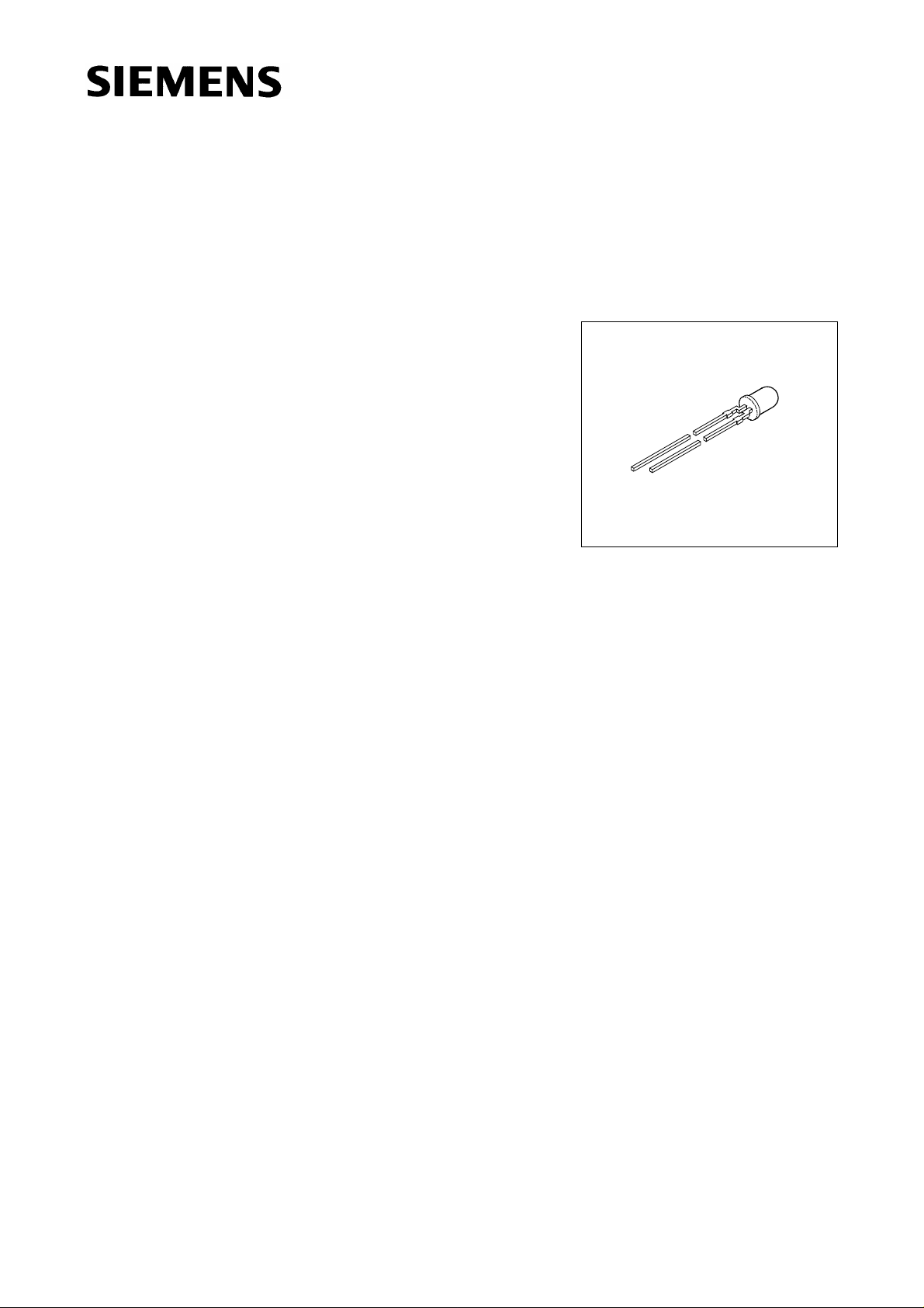
3 mm (T1) LED, Non Diffused LS 3340, LO 3340, LY 3340
LG 3330, LP 3340
Besondere Merkmale
● eingefärbtes, klares Gehäuse
● zur Einkopplung in Lichtleiter
● als optischer Indikator einsetzbar
● Lötspieße mit Aufsetzebene
● gegurtet lieferbar
● Störimpulsfest nach DIN 40839
Features
● colored, clear package
● optical coupling into light pipes
● for use as optical indicator
● solder leads with stand-off
● available taped on reel
● load dump resistant acc. to DIN 40839
VEX06710
Semiconductor Group 1 11.96
Page 2
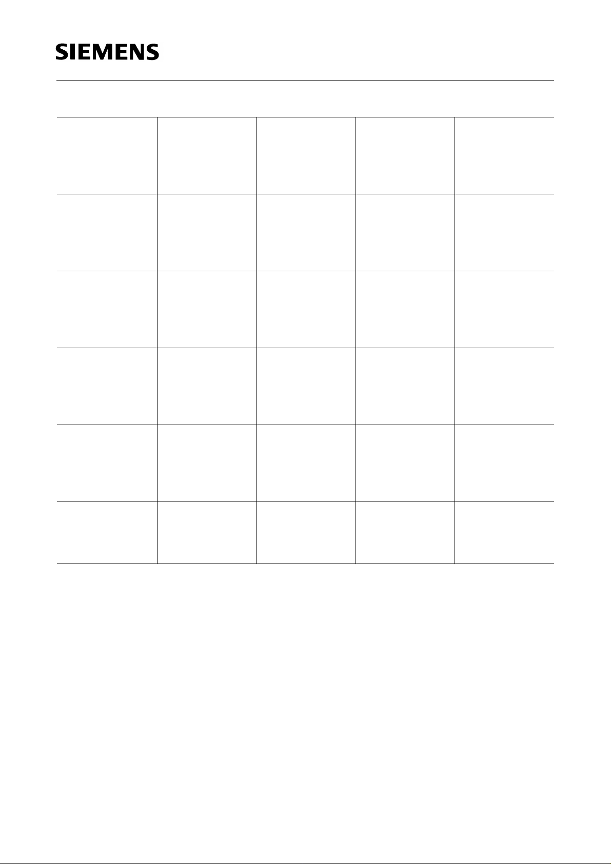
LS 3340, LO 3340, LY 3340
LG 3330, LP 3340
Typ
Type
LS 3340-KN
LS 3340-L
LS 3340-M
LS 3340-N
LS 3340-LP
LO 3340-KN
LO 3340-L
LO 3340-M
LO 3340-N
LO 3340-LP
LY 3340-JM
LY 3340-L
LY 3340-M
LY 3340-N
LY 3340-LP
Emissionsfarbe
Color of
Emission
Gehäusefarbe
Color of
Package
Lichtstärke
Luminous
Intensity
I
= 10 mA
F
I
(mcd)
V
super-red red clear 6.3 … 50.0
10.0 … 20.0
16.0 … 32.0
25.0 … 50.0
10.0 … 80.0
orange orange clear 6.3 … 50.0
10.0 … 20.0
16.0 … 32.0
25.0 … 50.0
10.0 … 80.0
yellow yellow clear 4.0 … 32.0
10.0 … 20.0
16.0 … 32.0
25.0 … 50.0
10.0 … 80.0
Bestellnummer
Ordering Code
Q62703-Q1701
Q62703-Q1702
Q62703-Q1704
Q62703-Q2320
Q62703-Q3223
Q62703-Q1886
Q62703-Q2256
Q62703-Q2255
Q62703-Q2473
Q62703-Q2628
Q62703-Q1789
Q62703-Q1791
Q62703-Q1999
Q62703-Q2652
Q62703-Q1792
LG 3330-KN
green colorless clear 6.3 … 50.0
LG 3330-L
LG 3330-M
LG 3330-N
LG 3330-LP
LP 3340-JL
pure green green clear 4.0 … 20.0
LP 3340-K
LP 3340-L
LP 3340-KM
Streuung der Lichtstärke in einer Verpackungseinheit
Luminous intensity ratio in one packaging unit I
V max
/ I
10.0 … 20.0
16.0 … 32.0
25.0 … 50.0
10.0 … 80.0
10.0 … 20.0
I
/ I
V max
≤ 2.0.
V min
6.3 … 12.5
6.3 … 32.0
≤ 2.0.
V min
Q62703-Q1698
Q62703-Q1699
Q62703-Q1700
Q62703-Q2010
Q62703-Q2011
Q62703-Q2749
Q62703-Q2982
Q62703-Q2980
Q62703-Q3211
Semiconductor Group 2
Page 3
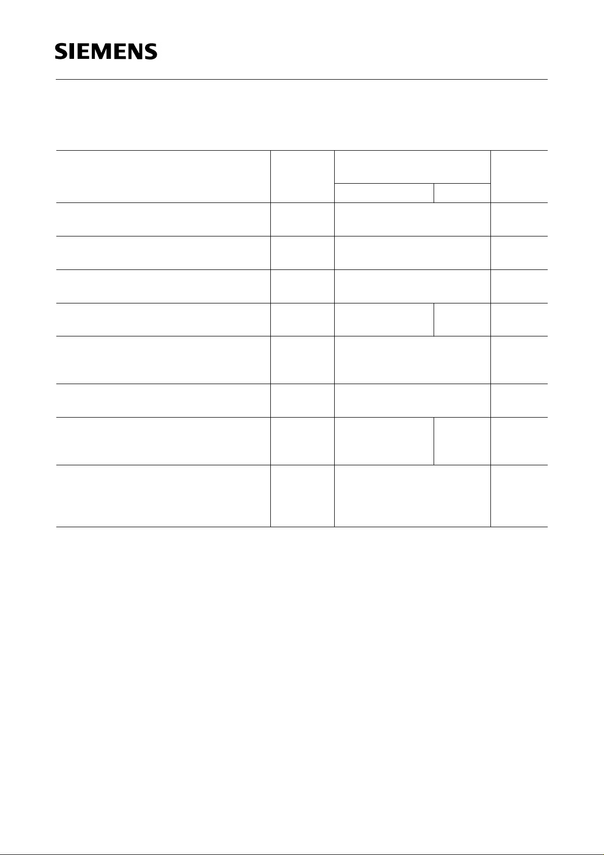
Grenzwerte
Maximum Ratings
LS 3340, LO 3340, LY 3340
LG 3330, LP 3340
Bezeichnung
Parameter
Betriebstemperatur
Operating temperature range
Lagertemperatur
Storage temperature range
Sperrschichttemperatur
Junction temperature
Durchlaßstrom
Forward current
Stoßstrom
Surge current
t ≤ 10 µs, D = 0.005
Sperrspannung
Reverse voltage
Verlustleistung
Power dissipation
T
≤ 25 ˚C
A
Wärmewiderstand
Thermal resistance
Sperrschicht / Luft
Junction / air
Symbol
Symbol
T
op
T
stg
T
j
I
F
I
FM
V
R
P
tot
R
th JA
Werte
Values
Einheit
Unit
LS, LO, LY, LG LP
–55…+100 ˚C
–55…+100 ˚C
+ 100 ˚C
40 30 mA
0.5 A
5V
140 100 mW
400 K/W
Semiconductor Group 3
Page 4

Kennwerte (TA = 25 ˚C)
Characteristics
LS 3340, LO 3340, LY 3340
LG 3330, LP 3340
Bezeichnung
Parameter
Wellenlänge des emittierten Lichtes (typ.)
Wavelength at peak emission (typ.)
I
= 20 mA
F
Dominantwellenlänge (typ.)
Dominant wavelength (typ.)
I
= 20 mA
F
Spektrale Bandbreite bei 50 %
Spectral bandwidth at 50 % I
I
= 20 mA
F
Abstrahlwinkel bei 50 %
Viewing angle at 50 % I
I
V
I
rel max
rel max
(Vollwinkel)
V
(typ.)
(typ.)
Durchlaßspannung (typ.)
Forward voltage (max.)
I
= 10 mA
F
Sperrstrom (typ.)
Reverse current (max.)
V
= 5 V
R
Kapazität (typ.)
Capacitance
V
= 0 V, f = 1 MHz
R
Schaltzeiten:
Switching times:
I
from 10 % to 90 % (typ.)
V
I
from 90 % to 10 % (typ.)
V
I
= 100 mA, tP = 10 µs, RL = 50 Ω
F
Symbol
Symbol
Werte
Values
Einheit
Unit
LS LO LY LG LP
λ
peak
λ
dom
635 610 586 565 557 nm
628 605 590 570 560 nm
∆λ 45 40 45 25 22 nm
2ϕ 50 50 50 50 50 Grad
deg.
V
V
I
I
C
t
t
F
F
R
R
0
r
f
2.0
2.6
2.0
2.6
2.0
2.6
2.0
2.6
2.0
2.6VV
0.01100.01100.01100.01100.0110µA
µA
128 101515pF
300
150
300
150
300
150
450
200
450
200nsns
Semiconductor Group 4
Page 5

LS 3340, LO 3340, LY 3340
LG 3330, LP 3340
Relative spektrale Emission I
= f (λ), TA= 25 ˚C, IF= 20 mA
rel
Relative spectral emission
V (λ) = spektrale Augenempfindlichkeit
Standard eye response curve
Abstrahlcharakteristik I
Radiation characteristic
= f (ϕ)
rel
Semiconductor Group 5
Page 6

LS 3340, LO 3340, LY 3340
LG 3330, LP 3340
Durchlaßstrom IF= f (VF)
Forward current
T
= 25 ˚C
A
Relative Lichtstärke IV/I
V(10 mA)
Relative luminous intensity
T
= 25 ˚C
A
= f (IF)
Zulässige Impulsbelastbarkeit IF= f (tP)
Permissible pulse handling capability
Duty cycle D = parameter, TA= 25 ˚C
LS, LO, LY, LG
Zulässige Impulsbelastbarkeit IF= f (tP)
Permissible pulse handling capability
Duty cycle D = parameter, TA= 25 ˚C
LP
Semiconductor Group 6
Page 7

LS 3340, LO 3340, LY 3340
LG 3330, LP 3340
Maximal zulässiger Durchlaßstrom
Max. permissible forward current
I
= f (TA)
F
Wellenlänge der Strahlung λ
Wavelength at peak emission
I
= 20 mA
F
peak
= f (TA)
Dominantwellenlänge λ
Dominant wavelength
I
= 20 mA
F
dom
= f (TA)
Durchlaßspannung VF= f (TA)
Forward voltage
I
= 10 mA
F
Semiconductor Group 7
Page 8

LS 3340, LO 3340, LY 3340
LG 3330, LP 3340
Relative Lichtstärke IV/I
V(25 °C)
Relative luminous intensity
I
= 10 mA
F
= f (TA)
Maßzeichnung (Maße in mm, wenn nicht anders angegeben)
Package Outlines (Dimensions in mm, unless otherwise specified)
Kathodenkennzeichnung: Kürzerer Lötspieß
Cathode mark: Short solder lead
GEX06951
Semiconductor Group 8
 Loading...