

Datasheet LNBP12SP, LNBP11SP, LNBP10SP, LNBP20PD, LNBP20CR Datasheet (SGS Thomson Microelectronics)
...Page 1
LNBP10 SERIES
LNB SUPPLY AND CONTROL VOLTAGE
REGULATOR (PARALLEL INTERFACE)
■ COMPLETEINTERFACE FOR TWOLNBs
REMOTE SUPPLYANDCONTROL
■ LNB SELECTIONAND STAND-BYFUNCTION
■ BUILT-INTONEOSCILLATORFACTORY
TRIMMEDAT22KHz
■ FASTOSCILLATORSTART-UP
FACILITATESDiSEqC ENCODING
■ TWOSUPPLY INPUTSFOR LOWEST
DISSIPATION
■ BYPASSFUNCTIONFOR SLAVE
OPERATION
■ LNB SHORTCIRCUIT PROTECTIONAND
DIAGNOSTIC
■ AUXILIARYMODULATIONINPUTEXTENDS
FLEXIBILITY
■ CABLELENGTHCOMPENSATION
■ INTERNALOVERTEMPERATURE
PROTECTION
■ BACKWARDCURRENT PROTECTION
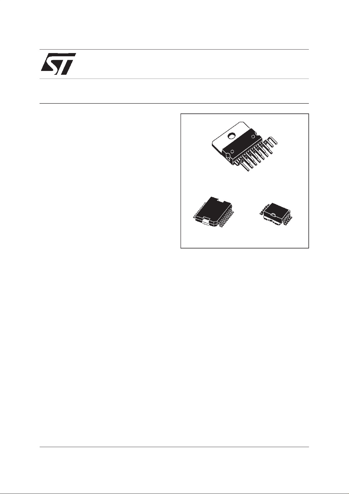
LNBP20
Multiwatt-15
10
1
PowerSo-20 PowerSO-10
DESCRIPTION
Intended for analog and digital satellite receivers,
the LNBP is a monolithic linear voltage regulator,
assembled in Multiwatt-15, PowerSO-20 and
PowerSO-10,specifically designed to provide the
powering voltages and the interfacing signals to
the LNB downconverter situated in the antenna
via the coaxial cable. Since most satellite
receivers have two antenna ports, the output
voltage of the regulator is available at one of two
logic-selectable output pins (LNBA, LNBB). When
the IC is powered and put in Stand-by (EN pin
LOW), both regulator outputs are disabled to
allow the antenna downconverters to be
supplied/controlled by others satellite receivers
sharing the same coaxial lines. In this occurrence
the device will limit at 3 mA (max) the backward
current that could flow from LNBA and LNBB
output pins to GND.
For slave operation in single dish, dual receiver
systems, the bypass function is implemented by
an electronic switch between the Master Input pin
(MI) and the LNBA pin, thus leaving all LNB
powering and control functions to the Master
Receiver. This electronic switch is closed when
the device is powered and EN pin is LOW.
The regulator outputs can be logic controlled to
be 13 or 18 V (typ.)by mean of the VSEL pin for
remote controlling of LNBs. Additionally, it is
possible to increment by 1V (typ.) the selected
voltage value to compensate the excess voltage
drop along the coaxial cable (LLC pin HIGH).
In order to reduce the power dissipation of the
device when the lowest output voltage is
selected, the regulator has two Supply Input pins
V
CC1
and V
. They must be powered
CC2
respectively at 16V (min) and 23V (min), and an
internal switch automatically will select the
suitable supply pin according to the selected
output voltage. If adequate heatsink is provided
and higher power losses are acceptable, both
supply pins can be powered by the same 23V
source without affecting any other circuit
performance.
The ENT (Tone Enable)pin activates the internal
oscillatorso that the DC output is modulatedby a
±0.3 V, 22KHz (typ.) square wave. This internal
oscillator is factory trimmed within a tolerance of
±2KHz, thus no further adjustments neither
externalcomponents are required.
A burst coding of the 22KHz tone can be
September 1998
1/18
Page 2
LNBP10 SERIES - LNBP20
accomplished thanks to the fast response of the
ENT input and the promptoscillator start-up. This
helps designers who want to implement the
DiSEqC protocols(*).
In order to improve design flexibility and to allow
implementation of newcoming LNB remote
control standards, an analogic modulation input
pin is available (EXTM). An appropriate DC
blocking capacitor must be used to couple the
modulatingsignal source to the EXTM pin. When
external modulation is not used, the relevant pin
canbe leftopen.
Two pins are dedicated to the overcurrent
protection/monitoring: CEXT and OLF. The
overcurrent protection circuit works dynamically:
as soon as an overloadis detectedin either LNB
output, the output is shut-down for a time Toff
determined by the capacitor connected between
CEXT and GND. Simultaneously the OLF pin,
from HIGH IMPEDANCE state goes LOW. After
the time has elapsed, the outputis resumedfor a
time t
=1/15t
on
(typ.) and OLF goes in HIGH
off
IMPEDANCE. If the overload is still present, the
protection circuit will cycle again through t
until the overload is removed. Typical ton+t
t
on
off
and
value is 1200ms when a 4.7µF external capacitor
is used.
This dynamic operation can greatly reduce the
power dissipation in short circuit condition, still
ensuring excellent power-on start up even with
highlycapacitiveloads on LNBoutputs.
The device is packaged in Multiwatt15 for
thru-holes mounting and in PowerSO-20 for
surface mounting. When a limited functionality in
a smaller package matches design needs, a
range of cost-effective PowerSO-10 solutions is
also offered. All versions have built-in thermal
protectionagainst overheatingdamage.
that is an open collector diagnostic output flag,
(*): External components are needed to comply to level 2.x and above (bidirectional) DiSEqC bus hardware requirements. DiSEqC is
a trademark of EUTELSAT.
ORDERING NUMBERS
Type Multiwatt-15 PowerSO-20 PowerSO-10
LNBP10
LNBP11
LNBP12
LNBP13
LNBP14
LNBP15
LNBP16
LNBP20 LNBP20CR LNBP20PD
LNBP10SP
LNBP11SP
LNBP12SP
LNBP13SP
LNBP14SP
LNBP15SP
LNBP16SP
off
PINCONFIGURATIONS
Multiwatt-15 PowerSO-20 PowerSO-10
2/18
Page 3

LNBP10 SERIES - LNBP20
TABLEA: PIN CONFIGURATIONS
SYMBOL NAME FUNCTION PIN NUMBER vs SALES TYPE(LNBP)
20CR 20PD 10SP 11SP 12SP 13SP 14SP 15SP 16SP
V
CC1
Supply Input 1 15V to25Vsupply. It is
121111111
automatically selected
=13or14V
OUT
232222222
V
CC2
whenV
Supply Input 2 22V to25Vsupply. It is
automatically selected
whenV
LNBA Output Port Seetruth tables forvoltage
=18or19V
OUT
343333333
and port selection. In
stand-bymode this port is
poweredby the MI pinvia
theinternal Bypass Switch
VSEL Output Voltage
Selection: 13 or
Logic control input: See
truthtable
454444444
18V (t yp)
EN Port Enable Logiccontrolinput: See
565555555
truthtable
OSEL Port Selection Logiccontrolinput: See
7 7 9 NANANANANANA
truthtable
GND Gr ound Circuit Ground.Itis
internally connected to the
dieframe
81
10
11
20
ENT 22 KHz Tone
Enable
CEXT External Capacitor Timingcapacitor used by
Logic control input: See
truthtable
9137777777
10148888888
theDynamicOverload
Protection.Typical
application is 4.7µFfora
1200ms cycle
EXTM External
Modulat i on
ExternalModulation Input.
Needs DC decoupling to
11 15 NA NA NA 9 NA 9 9
theAC source. If notused,
canbe leftopen.
LLC Line Length
Compens. (1V t yp)
OLF O ver Load F lag Logic output (open
Logic control input: See
truthtable
12 16 NA NA 9 NA 9 NA 10
13 17 NA 9 NA NA 10 10 NA
Collector). Normally in
HIGH IMPEDANCE,goes
LOW when current or
thermal overload occurs.
MI Master Input In stand-by mode, the
14 18 NA 10 10 10 NA NA NA
voltage onMI is routed to
LNBApin. Canbe left
openif bypass functionis
notneeded
LNBB Output Port Seetruth tables forvoltage
15 19 10 NA NA NA NA NA NA
and port selection.
NOTE: The limited pin availability of the PowerSO-10 package leads to drop some functions.
6666666
3/18
Page 4
LNBP10 SERIES - LNBP20
ABSOLUTE MAXIMUMRATING
Symbol Parameter Value Unit
V
DC InputVoltage(VCC1,VCC2,MI) 28 V
i
OutputCurrent (LNBA, LNBB) Internally limited
I
o
Logic InputVoltage (ENT, EN,OSEL, VSEL,LLC) -0.5 to 7 V
V
i
BypassSwitchCurrent 900 mA
I
SW
Power Dissipation at T
P
tot
StorageTemperature Range - 40 to 150
T
stg
Operating JunctionTemperature Range - 40 to 125
T
op
Absolute Maximum Ratings are those values beyond which damage to the device may occur. Functional operation under these conditions
is not implied
THERMAL DATA
Symbol Parameter Value Unit
R
thj-case
Thermal ResistanceJunction-case 2
LOGICCONTROLS TRUTH TABLES
Control I/O Pin Name L H
OUT OLF I
IN ENT 22KHz tone O F F 22KHz tone ON
IN EN See t a ble below S ee table below
IN OS EL See t a ble below S ee table below
IN V S E L See table below See table below
IN LLC See t a ble below S ee table below
<85oC14W
case
OUT>IOMAX
or Tj>150OCI
OUT<IOMAX
o
o
o
C/W
C
C
EN OSEL VSEL LLCP V
LXXX V
LNBA
-0.4V (t yp.) Disabled
MI
H L L L 13V (t yp.) Disabled
H L H L 18V (typ. ) Disabled
H L L H 14V (t yp.) Disabled
H L H H 19V (typ.) Disabled
H H L L Disable d 13V (typ.)
H H H L Disable d 18V (typ.)
H H L H Disabled 14V (typ.)
H H H H D isable d 19V (typ.)
NOTE: All logicinput pins have internal pull-down resistor (typ. = 250KΩ)
V
LNBB
4/18
Page 5
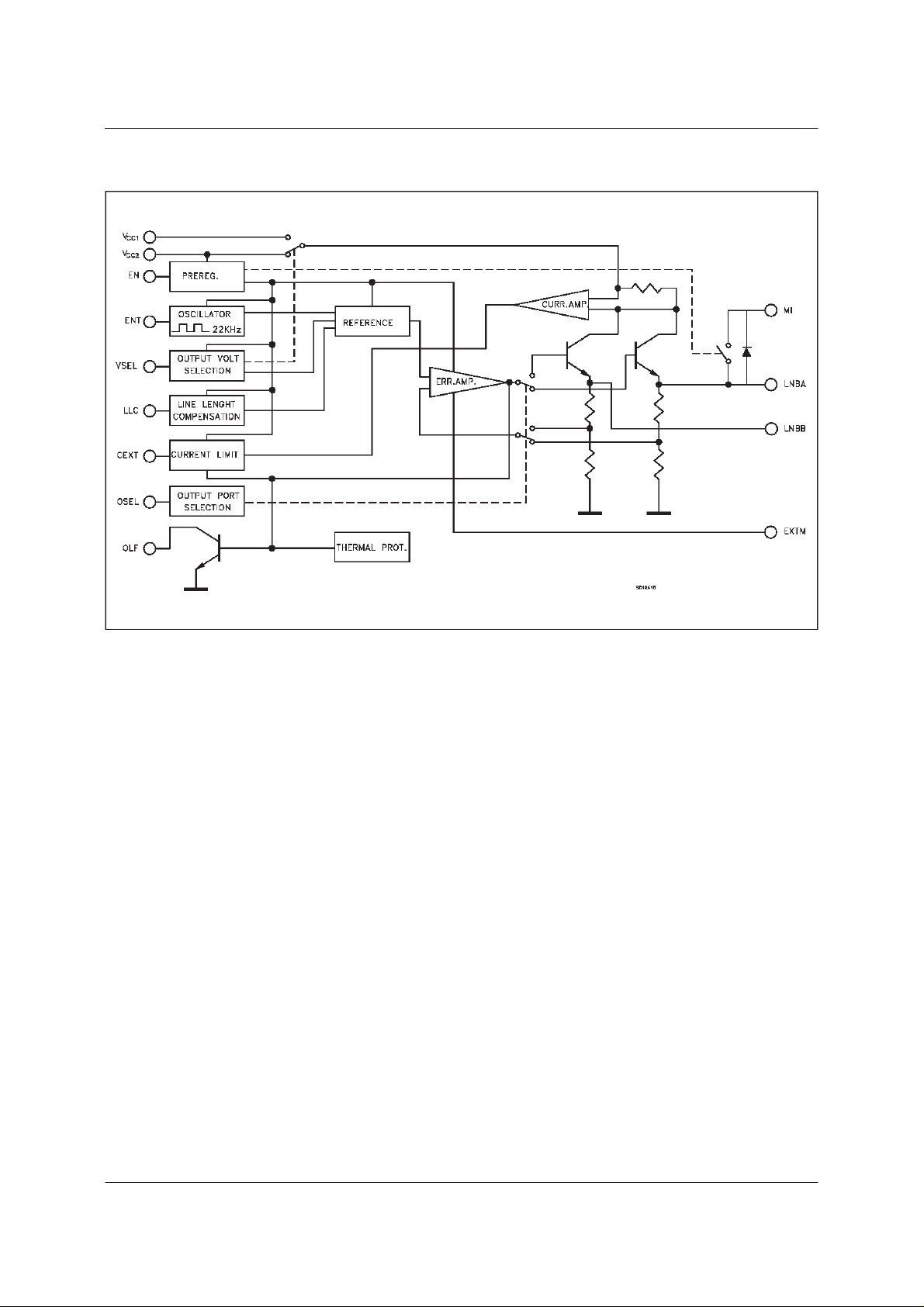
BLOCK DIAGRAM
LNBP10 SERIES - LNBP20
5/18
Page 6

LNBP10 SERIES - LNBP20
ELECTRICAL CHARACTERISTICS FOR LNBP SERIES (Tj=0 to85oC, Ci= 0.22 µF, Co= 0.1 µF,
EN=H,ENT=L, LLC=L,V
=16V,V
IN1
Symbol Parameter Test Conditions Min. Typ. Max. Unit
V
IN1VCC1
V
IN2VCC2
V
O1
V
O2
∆V
O
∆V
O
SupplyVoltage IO=500mA, ENT=H, VSEL=L, LLC=L
SupplyVoltage IO=500mA, ENT=VSEL=H, LLC=L
OutputVoltage IO=500 mA, VSEL=H, LLC=L
OutputVoltage IO=500 mA, VSEL=L, LLC=L
LineRegulation V
LoadRegulation V
SVR Supply VoltageRejection
I
t
OutputCurrent Limiting 500 650 800 mA
MAX
Dynamic Overload Protection
OFF
OFF Time
t
Dynamic Overload Protection
ON
ON Time
F
A
D
t
G
V
ToneFrequency ENT=H 20 22 24 KHz
TONE
ToneAmplitude ENT=H 0.4 0.6 0.8 Vpp
TONE
ToneDuty Cucle ENT=H 40 50 60 %
TONE
ToneRise or FallTime ENT=H 5 10 15 µs
r,tf
External Modulation Gain ∆
EXT M
External Modulation Input
EXTM
Voltage
Z
External Modulation
EXT M
Impedance
V
BypassSwitchVoltage Drop
SW
(MI toLNBA)
V
Overload FlagPinLogic Low IOL=8mA 0.28 0.5 V
OL
Overload FlagPinOFF State
I
OZ
Leakage Current
Control Input PinLogic Low 0.8 V
V
IL
Control Input PinLogic High 2.5 V
V
IH
Control Pins Input Current VIH=5V 20 µA
I
IH
Supply Current OutputsDisabled (EN=L) 0.3 1 mA
I
CC
Supply Current ENT=H, I
I
CC
I
T
OutputBackward Current EN=L, V
OBK
Thermal ShutdownThreshold 150
SHDN
IN2
=23V,I
=50mA, (unless otherwisespecified)
OUT
25
=500mA, ENT=H, VSEL=L, LLC=H1516
I
O
=500mA, ENT=VSEL=H, LLC=H
I
O
=500 mA, VSEL=H, LLC=H
I
O
I
=500 mA, VSEL=L, LLC=H
O
=15to18V, V
IN1
=22to25V, V
V
IN2
IN1=VIN2
=50to500mA
I
O
V
IN1=VIN2
=22V, V
=23± 0.5Vac,fac=50 KHz
Outputshorted, C
Outputshorted, C
/∆V
V
OUT
, f = 10Hzto 40KHz
EXTM
OUT
OUT
EXT
EXT
=13V
=18V
= 13 or 18V,
OUT
=4.7µF
=4.7µF
22
23
17.3 18
19
12.5 13
14
80 180 mV
45 dB
1100 ms
t
OFF
4
4
/15 ms
5
25
25
25
18.7 V
13.5 V
40
40
AC Coupling 400 mV
f = 10Hzto 40KHz 400 Ω
EN=L, ISW=300mA, V
= 4V 0.35 0.6 V
CC2-VMI
VOH=6V 10 µA
= 500mA 3.1 6 mA
OUT
0.23mA
V
IN1=VIN2
LNBA=VLNBB
=22V or floating
=18V
V
V
V
V
V
V
mV
mV
o
C
pp
6/18
Page 7

LNBP10 SERIES - LNBP20
TYPICALPERFORMANCE CHARACTERISTICS (unlessotherwisespecified T
OutputVoltagevs Output Current
Tone Duty Cycle vs Temperature
Tone Frequencyvs Temperature
ToneRise Time vs Temperature
=25oC)
j
Tone Fall Time vs Temperature
ToneAmplitude vs Temperature
7/18
Page 8

LNBP10 SERIES - LNBP20
TYPICALPERFORMANCE CHARACTERISTICS (continued)
S.V.R. vs Frequency
LNBAExternal Modulation Gain vs Frequency
ExternalModulation vs Temperature BypassSwitch Drop vs OutputCurrent
Bypass SwitchDrop vs Output Current
8/18
OverloadFlag pin Logic Low vs Flag Current
Page 9

TYPICALPERFORMANCE CHARACTERISTICS (continued)
LNBP10 SERIES - LNBP20
Supply Currentvs Temperature
DynamicOverloadprotection (I
SupplyCurrent vs Temperature
vs Time) ToneEnable
SC
Tone Disable
22 KHz Tone
9/18
Page 10

LNBP10 SERIES - LNBP20
TYPICALPERFORMANCE CHARACTERISTICS (continued)
EnableTime
DisableTime
18V to 13V Change 13V to 18V Change
10/18
Page 11

TYPICALAPPLICATIONSCHEMATICS
TWOANTENNA PORTS RECEIVER
10uF
C2
AUX DATA
R1
47K
11
13
4
9
5
7
12
EXTM
OLF
VSEL
ENT
EN
OSEL
LLC
LNBP20CR
VCC1
VCC2
LNBA
LNBB
CEXT
GND
LNBP10 SERIES - LNBP20
17V 24VMCU+V
1
2
3
15
14
MI
10
C14.7µFC4C6C5
+
8
C3
2x 0.1µF
2x 47nF
TUNER
ANT CONNECTORS
JA
JB
I/OsVcc
MCU
SINGLEANTENNA RECEIVERWITHMASTER RECEIVER PORT
24V17V
C4 C5
C3
47nF
AUX DATA
MCU+V
R1
47K
10uF
C2
11
EXTM
13
OLF
4
VSEL
9
ENT
5
EN
7
OSEL
12
LLC
LNBP20CR
VCC1
VCC2
LNBA
LNBB
CEXT
GND
1
2
3
15
14
MI
10
4.7µF
C1
+
8
2x 0.1µF
I/Os
ANT
MASTER
TUNER
I/OsVcc
MCU
I/Os
11/18
Page 12

LNBP10 SERIES - LNBP20
TYPICALAPPLICATIONSCHEMATICS (continued)
USINGSERIAL BUS TO SAVE MPU I/Os
MCU+V
R1
47K
I/Os Vcc
AUX DATA
1
STR
2
D
3
CLK
15
OE
4094
MCU+V
17V 24V
C2
11
EXTM
10uF
13
OLF
4
4
Q1
5
Q2
6
Q3
7
Q4
14
Q5
13
Q6
12
Q7
11
Q8
9
QS
10
QS
9
5
7
12
MCU
VSEL
ENT
EN
OSEL
LLC
LNBP20CR
VCC1
VCC2
LNBA
LNBB
CEXT
GND
1
2
3
15
14
MI
10
8
4.7µF
C1
+
C3
2x 0.1µF
C4 C6C5
2x 47nF
SERIAL
BUS
TUNER
ANT
CONNECTORS
JA
JB
TWOANTENNA PORTS RECEIVER:LOWCOSTSOLUTION
17V 24V
1
VCC1
2
VCC2
3
LNBA
10
LNBB
CEXT
GND
8
C14.7µFC4C6C5
+
6
MCU
C3
2x 0.1µF
2x 47nF
MCU+V
4
VSEL
7
ENT
5
EN
9
OSEL
LNBP10SP
I/OsVcc
ANT CONNECTORS
JA
JB
TUNER
I/Os
12/18
Page 13

TYPICALAPPLICATIONSCHEMATICS (continued)
LNBP10 SERIES - LNBP20
CONNECTINGTOGETHER V
4
VSEL
7
ENT
5
EN
9
OSEL
MCU+V
I/OsVcc
LNBP10SP
CC1
VCC1
VCC2
LNBA
LNBB
CEXT
ANDV
GND
1
2
3
10
8
6
4.7µF
MCU
CC2
24V
ANT CONNECTORS
JA
JB
TUNER
C1
C4
+
0.1µF
C6C5
2x 47nF
I/Os
SINGLEANTENNA RECEIVERWITHMASTER RECEIVER PORT:LOW COST SOLUTION
24V17V
C2
AUX DATA
MCU+V
9
EXTM
10µF
4
VSEL
7
ENT
5
EN
LNBP13SP
I/OsVcc
VCC1
VCC2
LNBA
CEXT
GND
1
2
3
10
MI
8
C4 C5
C3
C14.7µF
+
6
2x 0.1µF
MCU
47nF
TUNER
I/Os
ANT
MASTER
13/18
Page 14

LNBP10 SERIES - LNBP20
TYPICALAPPLICATIONSCHEMATICS (continued)
SINGLEANTENNA RECEIVERWITHOVERLOAD DIAGNOSTIC
AUX DATA
MCU+V
R1
47K
Vcc I/Os
10µF
24V17V
C2
9
10
4
7
5
EXTM
OLF
VSEL
ENT
EN
LNBP15SP
VCC1
VCC2
LNBA
CEXT
GND
1
2
3
8
C14.7µF
+
6
MCU
C3
2x 0.1µF
C4 C5
47nF
TUNER
I/Os
ANT
14/18
Page 15

LNBP10 SERIES - LNBP20
MULTIWATT-15 MECHANICAL DATA
DIM.
A 5 0.197
B 2.65 0.104
C 1.6 0.063
D 1 0.039
E 0.49 0.55 0.019 0.022
F 0.66 0.75 0.026 0.030
G 1.02 1.27 1.52 0.040 0.050 0.060
G1 17.53 17.78 18.03 0.690 0.700 0.710
H1 19.6 0.772
H2 20.2 0.795
L 21.9 22.2 22.5 0.862 0.874 0.886
L1 21.7 22.1 22.5 0.854 0.870 0.886
L2 17.65 18.1 0.695 0.713
L3 17.25 17.5 17.75 0.679 0.689 0.699
L4 10.3 10.7 10.9 0.406 0.421 0.429
L7 2.65 2.9 0.104 0.114
M 4.25 4.55 4.85 0.167 0.179 0.191
M1 4.63 5.08 5.53 0.182 0.200 0.218
S 1.9 2.6 0.075 0.102
S1 1.9 2.6 0.075 0.102
Dia1 3.65 3.85 0.144 0.152
MIN. TYP. MAX. MIN. TYP. MAX.
mm inch
0016036
15/18
Page 16

LNBP10 SERIES - LNBP20
PowerSO-20 MECHANICAL DATA
DIM.
MIN. TYP. MAX. MIN. TYP. MAX.
mm inch
A 3.60 0.1417
a1 0.10 0.30 0.0039 0.0118
a2 3.30 0.1299
a3 0 0.10 0 0.0039
b 0.40 0.53 0.0157 0.0209
c 0.23 0.32 0.009 0.0126
D (1) 15.80 16.00 0.6220 0.6299
E 13.90 14.50 0.5472 0.570
e 1.27 0.050
e3 11.43 0.450
E1 (1) 10.90 11.10 0.4291 0.437
E2 2.90 0.1141
G 0 0.10 0 0.0039
h 1.10 0.0433
L 0.80 1.10 0.0314 0.0433
N10
S8
o
(max.)
o
(max.)
T 10.0 0.3937
(1)”D and E1” do not include mold flash or protusions
-Mold flash or protusions shall not exceed 0.15mm (0.006”)
E2
hx45°
NN
a2
A
b
DETAILA
110
e3
D
T
e
1120
E1
R
DETAILB
PSO20MEC
lead
a3
Gage Plane
E
DETAILB
0.35
S
L
c
a1
DETAILA
slug
-C-
SEATINGPLANE
GC
(COPLANARITY)
0056635
16/18
Page 17

LNBP10 SERIES - LNBP20
PowerSO-10MECHANICAL DATA
DIM.
mm inch
MIN. TYP. MAX. MIN. TYP. MAX.
A 3.35 3.65 0.132 0.144
A1 0.00 0.10 0.000 0.004
B 0.40 0.60 0.016 0.024
c 0.35 0.55 0.013 0.022
D 9.40 9.60 0.370 0.378
D1 7.40 7.60 0.291 0.300
E 9.30 9.50 0.366 0.374
E1 7.20 7.40 0.283 0.291
E2 7.20 7.60 0.283 0.300
E3 6.10 6.35 0.240 0.250
E4 5.90 6.10 0.232 0.240
e 1.27 0.050
F 1.25 1.35 0.049 0.053
H 13.80 14.40 0.543 0.567
h 0.50 0.002
L 1.20 1.80 0.047 0.071
q 1.70 0.067
α 0
o
o
8
==
==
HE
h
A
F
A1
610
51
eB
M
0.25
D
==
D1
==
E2
==
DETAIL”A”
DETAIL”A”
Q
B
0.10 A
E1E3
==
SEATING
PLANE
A
C
α
B
E4
==
SEATING
PLANE
A1
L
==
0068039-C
17/18
Page 18

LNBP10 SERIES - LNBP20
Information furnished is believed to be accurate andreliable. However, STMicroelectronics assumes no responsibility forthe consequences
of use of such information nor for any infringement of patents or other rights of third parties which may result from its use. No license is
granted by implication or otherwise under any patent or patent rights of STMicroelectronics. Specification mentioned in this publication are
subject to change without notice. This publication supersedes and replaces all information previously supplied. STMicroelectronics products
are not authorizedfor use as critical components in life support devices or systems without express written approval of STMicroelectronics.
The ST logo is a trademark of STMicroelectronics
1998 STMicroelectronics – Printed in Italy –All Rights Reserved
STMicroelectronics GROUP OF COMPANIES
Australia - Brazil -Canada - China - France - Germany - Italy - Japan - Korea - Malaysia - Malta - Mexico- Morocco- TheNetherlands -
18/18
Singapore - Spain - Sweden - Switzerland - Taiwan - Thailand -United Kingdom - U.S.A.
.
 Loading...