

Page 1
LNBH21
LNB SUPPLY AND CONTROL IC WITH
STEP-UP CONVERTER AND I
■ COMPLETE INTERFACE BETWEEN LNB
■ BUILT-IN DC/DC CONTROLLER FOR
■ TWO SELECTABLE OUTPUT CURRENT
■ BOTH COMPLIANT WITHEUTELSAT AND
■ ACCURATE BUILT-IN 22KHz TONE
■ FASTO SCILLATOR START-UP FACILITATES
■ BUILT-IN 22KHz TO NE DETECTOR
■ SEMI-LOWDROP POSTREGULATOR AND
■ TWO OUTPUT PINS SUITABLE TO BYPASS
■ CABLE LENGTH DIGITAL COMPENSATION
■ OVERLOAD AND OVER-TEMPERATURE
2CTM
AND I
BUS
SINGLE 12V SUPPLY OPERATION AND
HIGH EFFICIENCY (Typ. 94% @ 750mA)
LIMIT (450m A / 750mA)
DIRECT OUTPUT VOLTAGE
SPECIFICATION
OSCILLATOR SUITS WIDELY ACCEPTED
STANDARDS
DiSEqC
SUPPORTS BI-DIRECTIONAL DiSEqC
TM
ENCODING
TM
2.0
HIGH EFFICIENCY STEP-UP PWM FOR
LOW POWE R LOSS: Typ. 0.56W @ 125mA
THE OUTPUT R-L FILTER AND AVOID ANY
TONE DISTORSION (R-L FILTER AS PER
DiSEqC 2.0 SPECs, see application circuit on
pag. 5)
INTERNAL PROTECTIONS
2
C INTERFACE
PowerSO-20
■ OVERLOADANDOVER-TEMPERATUREI
2
C
DIAGNOSTIC BITs
■ LNB SHORT CIRCUIT SOA PROTECTION
WITHI
■ +/- 4KV ESD TOLERANTON INPUT/
2
C DIAGNOSTIC BIT
OUTPUT POWER PINS
DESCRIPTION
Intended for analog and digital satellite STB
receivers/SatTV, sets/PC cards, t he LNBH 21 is a
monolithic voltage regulator and interface IC,
assembled in POWER SO-20, specifically
designed to provide the 13/1 8V power supply and
the 22KHz tone signalling to the LNB
downconverter in the antenna or to the multiswitch
box. In this application field, it off ers a complete
solution with extremely low component count, low
power dissipation together with simpl e des ign and
2CTM
I
standard interfacing.
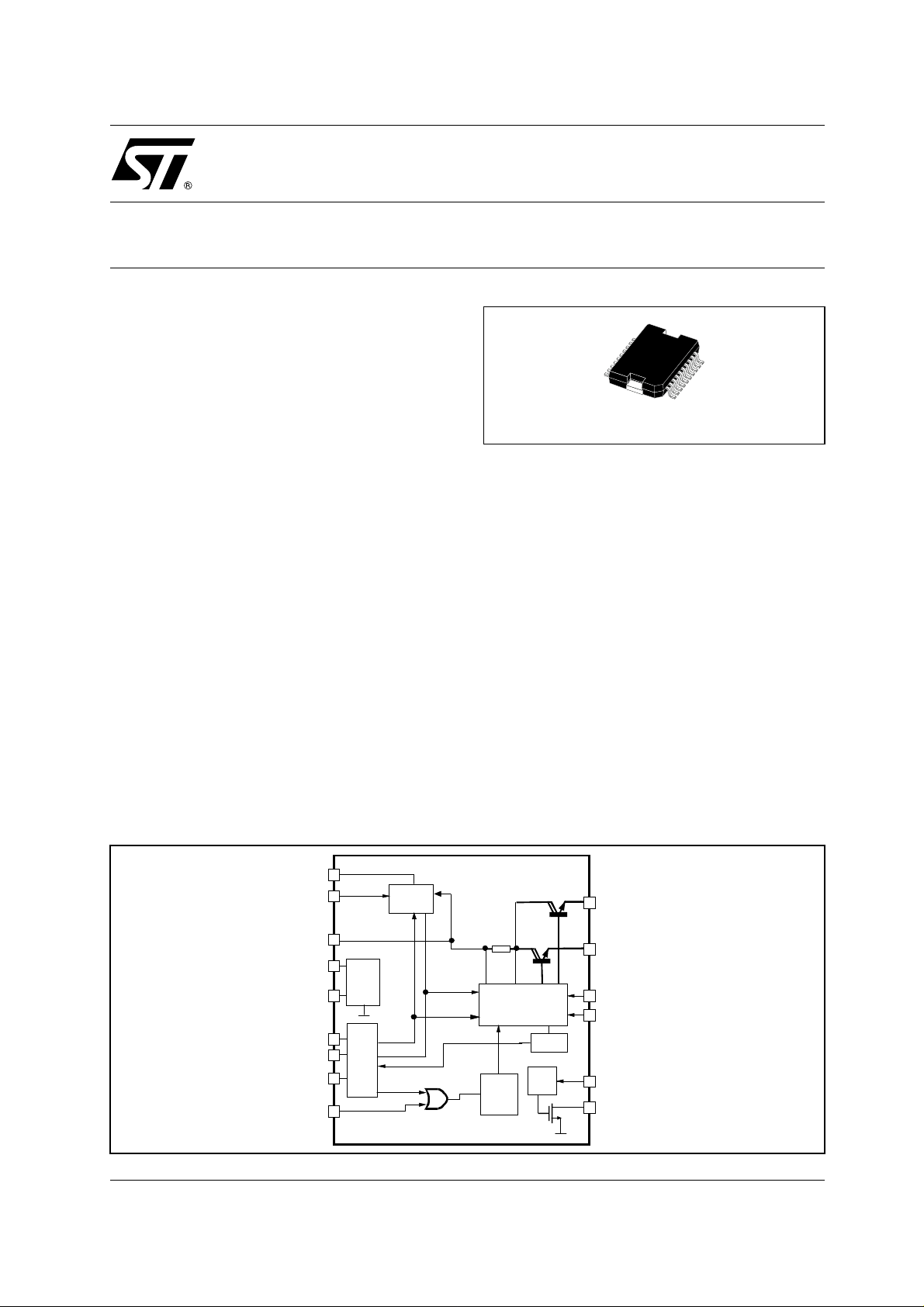
BLOCK DIAGRAM
Gate
Sense
Vup
Vcc
Byp
SDA
SCL
ADDR
DSQIN
Preregul.+
U.V.lockout
+P.ON res.
I²C interf.
V Select
Enable
TEN
Step-up PWM
Controller
LNBH21
Vup-Feedback
Linear Post-reg
+Protections
22KHz
Oscil l.
+Modulator
Diagnostics
T one
Detec tor
VoTX
VoRX
ISEL
EXTM
DETIN
DSQOUT
1/20April 2004
Page 2
LNBH21
ORDERING CODES
TYPE
PowerSO-20
(Tube)
PowerSO-20
(Tape & Reel)
LNBH21 LNBH21PD LNBH21PD-TR
ABSOLUTE MAXIMUM RATINGS
Symbol Parameter Value Unit
V
V
I
V
TX/RX DC Output Pins Voltage
O
V
V
DETIN
V
I
GATE
V
SENSE
V
ADDRESS
T
T
Absolute Maximum Ratings are those values beyond which damage to the device may occur. Functional operation under these condition is
not implied.
DC Input Voltage
CC
DC Input Voltage
UP
Output Current
O
Logic Input Voltage (SDA, SCL, DSQIN, ISEL)
I
Detector Input Signal Amplitude
Logic High Output Voltage (DSQOUT)
OH
Gate Current
Current Sense Voltage
Address Pin Voltage
Storage Temperature Range
stg
Operating Junction Temperature Range
op
-0.3 to 16 V
-0.3 to 25 V
Internally Limited mA
-0.3 to 25 V
-0.3 to 7 V
-0.3 to 2
V
PP
-0.3 to 7 V
±400 mA
-0.3 to 1 V
-0.3 to 7 V
-40 to +150 °C
-40 to +125 °C
THERMAL DATA
Symbol Parameter Value Unit
R
thj-case
Thermal Resistance Junction-case
2°C/W
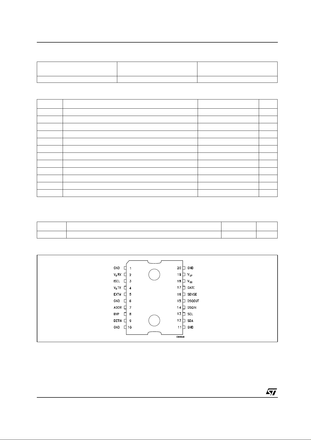
PIN CONFIGUARATION (top view)
2/20
Page 3
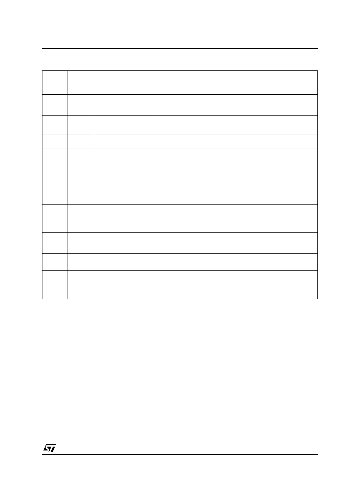
TABLE A: PIN CONFIGURATIONS
PIN N° SYMBOL NAME FUNCTION
18 V
17 GATE External Switch Gate External MOS switch Gate connection of the step-up converter
16 SENSE Current Sense Input DC/DC Current Sense comparator input. Connected to current
19 V
2V
O
12 SDA Serial Data
13 SCL Serial Clock
14 DSQIN DiSEqC Input When the TEN bit of the System Register is LOW, this pin will accept
9 DETIN Tone Detector Input 22kHz Tone Detector Input. Must be AC coupled to the DiSEcQ 2.0
15 DSQOUT DiSEqC Output Open drain output of the tone Detector to the main µcontroller for
5 EXTM External Modulator External Modulation Input acts on V
1, 6, 10,
GND Ground Pins Connected to Ground.
11, 20
8 BYP Bypass Capacitor Needed for internal preregulator filtering
3 ISEL Current Limit Select Set high or floating for Iout<=750mA, connect to ground for
4V
O
7 ADDR Address Setting
Supply Input 8V to 15V IC supply. A 220µF bypass capacitor to GND with a 470nF
CC
(ceramic) in parallel is recommended
sensing resistor
Step-up Voltage Input of the linear post-regulator. The voltage on this pin is monitored
UP
by internal step-ut controller to keep a minimum dropout across the
linear pass transistor
RX Output Port during
22KHz Tone RX
RX Output to the LNB in DiSEqC 2.0 application. See truth tables for
voltage selections on page 8 and description on page 5.
Bidirectional data from/to I
2
Clock from I
C bus.
2
C bus.
the DiSEqC code from the main µcontroller. The LNBH21 will use this
code to modulate the internally generated 22kHz carrier. Set to GND
this pin if not used.
bus.
DiSEcQ 2.0 data decoding. It is LOW when tone is detected.
TX. Needs DC decoupling to the
O
AC source. If not used, can be left open.
I
≤ 450mA.
OUT
TX Output Port during
22KHz Tone TX
Output of the linear post-regulator/modulator to the LNB. See truth
tables for voltage selections.
2
Four I
C bus addresses available by setting the Address Pin level
voltage. See address pin characteristics table.
LNBH21
3/20
Page 4
LNBH21
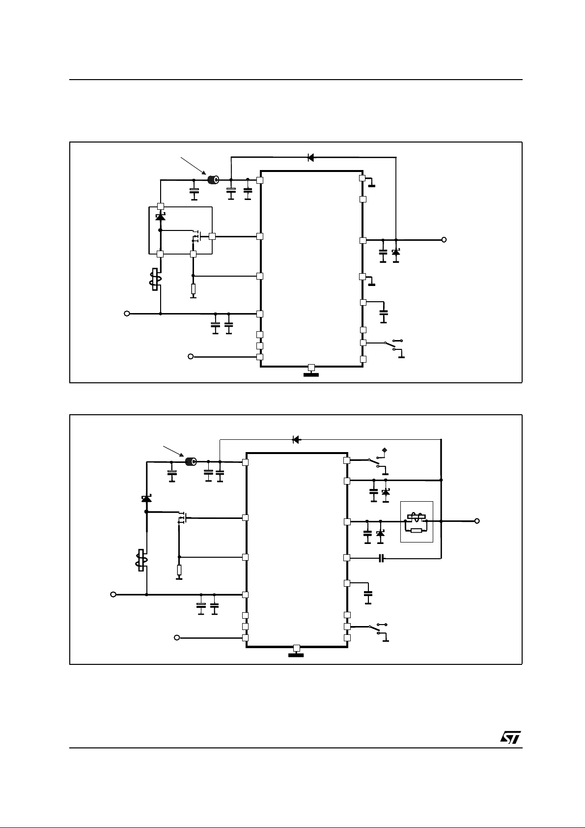
TYPICAL APPLICATION CIRCUITS
Application Circuit fo r Di S EqC 1.x and Output Current < 450 mA
D1 1N4001
FerriteBead Filter
FerriteBead Filter
F1 suggested part number:
F1 suggested part number:
MURATABL01RN1-A62
MURATABL01RN1-A62
Panasonic EXCELS A35
Panasonic EXCELS A35
IC2
IC2
L1=22µH
L1=22µH
Vin
Vin
12V
12V
ToneEnable
ToneEnable
C2
C2
220µF
220µFC2220µF
STS4DNFS30L
STS4DNFS30L
Rsc
Rsc
Ω
Ω
0.1ΩΩΩ
0.1ΩΩΩ
C1
C1
220µF
220µF
F1
F1
C9
C9
100µF
100µF
SENSE
SENSE
C4(***)
C4(***)
470nF
470nF
Ceramic
Ceramic
DSQIN(**)
DSQIN(**)
Vup
Vup
C3(***)
C3(***)
470nF
470nF
Ceramic
Ceramic
GATE
GATE
SDA
SDA
SCL
SCL
IC1
IC1
19
19
17
17
16
16
18
18
12
12
13
13
14
14
D1 1N4001
LNBH21
LNBH21
GND
GND
3
3
2
2
4
4
9
9
8
8
5
5
7
7
15
15
ISEL
ISEL
VoRX
VoRX
VoTX
VoTX
C8(***)
C8(***)
10nF
10nF
(**) DETIN
(**) DETIN
Byp
Byp
EXTM
EXTM
Address
Address
DSQOUT
DSQOUT
Set TTX =1
Set TTX =1
D2(***)
D2(***)
BAT43
BAT43
C5
C5
470nF
470nF
0<VADDR<VBYP
0<VADDR<VBYP
to LNB
to LNB
Full Application Circuit for Bi-directional DiSEqC 2.0 and Output Current up to 750mA
F1 suggested part number:
F1 suggested part number:
F1 suggested part number:
F1 suggested part number:
MURATABL01RN1-A62
MURATABL01RN1-A62
MURATABL01RN1-A62
MURATABL01RN1-A62
Panasonic EXCELS A35
Panasonic EXCELS A35
Panasonic EXCELS A35
Panasonic EXCELS A35
AxialFerriteBead Filter
AxialFerriteBead Filter
AxialFerriteBead Filter
AxialFerriteBead Filter
F1
F1
F1
C2
C2
C2
220µF
220µF
220µFC2220µF
D1
D1
D1
1N5821 or
1N5821 or
1N5821 or
STPS3L40A
STPS3L40A
STPS3L40A
L1=22µH
L1=22µH
L1=22µH
Vin
Vin
Vin
12V
12V
12V
(*) Filter to be used according to EUTELSAT recommendation to implement the DiSEqCTM2.0,(see DiSEqCTMimplementation on page 8).
If bidirectionalDiSEqC
Rsc
Rsc
Rsc
0.05
0.05
0.05
22KHz Tone Enable
22KHz Tone Enable
TM
2.0 is not implemented it can be removed both with C8 and D4.
ΩΩΩΩ
ΩΩΩΩ
ΩΩΩΩ
100µF
100µF
100µF
MOS
MOS
MOS
STN4NF03L
STN4NF03L
STN4NF03L
C1
C1
C1
220µF
220µF
220µF
C9
C9
C9
C3(***)
C3(***)
C3(***)
470nF
470nF
470nF
Ceramic
Ceramic
Ceramic
C4(***)
C4(***)
C4(***)
470nF
470nF
470nF
Ceramic
Ceramic
Ceramic
IC1
IC1
IC1
Vup
Vup
Vup
Gate
Gate
Gate
Sense
Sense
Sense
Vcc
Vcc
Vcc
SDA
SDA
SDA
SCL
SCL
SCL
DSQIN (** )
DSQIN (** )
DSQIN (** )
(**) Do not leave these pins floating if not used.
(***) To be soldered as close as possible to relative pins.
-C8 and D3,4 are needed only to protect the output pins from any negative voltage spikes during high speed voltage transitions.
D2 1N4001
D2 1N4001
D2 1N4001
LNBH21
LNBH21
LNBH21
GND
GND
GND
ISEL
ISEL
ISEL
VoTX
VoTX
VoTX
VoRX
VoRX
VoRX
(**)DETIN
(**)DETIN
(**)DETIN
Byp
Byp
Byp
EXTM
EXTM
EXTM
ADDRESS
ADDRESS
ADDRESS
DSQOUT
DSQOUT
DSQOUT
C8(***)
C8(***)
C8(***)
100nF
100nF
100nF
C7(***)
C7(***)
C7(***)
100nF
100nF
100nF
Floating or V>3.3V
Floating or V>3.3V
Floating or V>3.3V
Higher current limit
Higher current limit
Higher current limit
Lower current limit
Lower current limit
Lower current limit
GND
GND
GND
D4(***)
D4(***)
D4(***)
BAT43
BAT43
BAT43
D3(***)
D3(***)
D3(***)
BAT43
BAT43
BAT43
(*) see note
(*) see note
(*) see note
C6
C6
C6
10nF
10nF
10nF
C5
C5
C5
470nF
470nF
470nF
0<V
0<V
0<V
0<V
270µH
270µH
270µH
15 ohm
15 ohm
15 ohm
ADDR<VBYP
ADDR<VBYP
ADDR<VBYP
ADDR<VBYP
to LNB
to LNB
to LNB
4/20
Page 5

LNBH21
APPLICATION INFORMATION
This I C has a built in DC/DC step-up controller that, from a single su pply source ranging from 8 to 15V,
generates t he voltages (V
1.65W typ. @ 750mA load (the linear regulator drop vol tage is internally kept at: V
UnderVoltage Lockout circuit will disable the whole circuit when the supplied V
threshold (6.7V typically). The internal 22KHz tone generator is factory trimmed in accordanc e to the
standards, and can be controlled either by the I
immediate DiSEqC
TM
continuous 22KHz tone is generate d on the output regardless of the DSQI N pin logic status.
The TE N bit must be set LOW when the DSQIN pin is used for DiSEqC
bi-directional DiSEqC
(DETIN) must be AC coupled to the DiSEqC
DSQOUT pin (*).
To comply to the bi-directional DiSEqC
The LNBH21 is prov ided with two output pins: the V
V
RX to be used when the tone is recei v ed. This allows the 22KHz Tone to pass without any losses due
O
to the R-L filter impedanc e (see DiSeqC 2.0 applica tio n circuit on page 5). In DiSeqC 2.0 applications
during the 22K Hz trans mi ssio n activated by DSQIN pin (or TEN I
preventively set ON by the TTX I
provided by mean of V
OFF by setting the TTX I
pin through the R-L filter. When the LNBH21 is used in DiSeqC 1.x applications the R-L filter is not
required (see D iS eqC 1.x application circuit on pag.5 ), the TTX I
that, the V
TX output pin can provide both the 13/18V power supply and the 22KHz tone, enable d by
O
DSQIN pin or by TEN I
All the functions of this IC are controlled via I
bits). The same registercan be read back, and two bits will report the diagnos tic statu s. When the ICis put
in Stand-by (EN bit LOW), t he power blocks are disabled. When the regulator blocks are active (EN bit
HIGH), the output can be logic controlled to be 13 or 18 V by m ean of the V
remote controlling of non-DiSEqC LNBs.
Additionally, the LNBH21 is provided with the LLC I
when V
=0 and +1.5V when V
SEL
cable (LLC bit HIGH).
By mean of t he LLC bit, the LNBH21 is also compliant to the American LNB power supply standards that
require the higher output voltage level to 19.5V (typ.) (instead of 18V), by s im ply setting the LLC=1 wh en
V
=1.
SEL
In order to improve design flexibility and to allow implementation of newcoming LNB remote control
standards, an analogic modulation input pin is available (EXT M). An appropriate DC blocking capacitor
must be used to couple the mod ulat ing signal source to the EXTM pin. Also in this case, the V
must be set ON during the tone transmission by setting the TTX bit high. When external modulation is not
used, the relevant pin can be left open.
The current limitation block is SOA type and it is possible to selec t two current limit threshold s, by the
dedicated I
pin. The higher threshold is in the range of 750mA to 1A if the I
SEL
connected a voltage > 3.3V. The lower threshold is in the range of 450mA to 70 0mA when the I
connected to ground. When theoutput port is shorted to ground, theSOA current limitation block limits the
shortcircuit current (I
SC
dissipation. Moreover, it is possible to set t he Short Circuit Current protection either statically (simple
current clamp) or dynami ca lly by t he P CL bit of the I
set to LOW, the overcurrent protection circuit works dynamically, as soon as an overload is detected, the
output is shut-down for a time T
is set to HIGH. After this time has elapsed, the output is resumed for a tim e T
endof T
the end of a full T
, i f the overload is stilldetected, the protection circuit will cycle again through T
ON
ON
resettoLOW.TypicalT
operation can greatly reduce the power dissipation in short circuit condition, still ensuring excellent
power-on start up in most conditions.
) that let the linear post-regulator to work at a minimum dissipated power of
UP
CC
2CTM
interface or by a dedicated pin (DSQIN) that allows
=2.2V typ.). An
UP-VO
drops below a fixed
data en co ding (*). When the TEN (Tone E N able) I2C bit it is set to HIGH, a
TM
TM
2.0 interfacing is completed by the built-in 22KHz tone detector. Its input pin
2
C bit and, both the 13/18V power supply and the 22KHz tone, are
TX output. A s soon as the tone transmission is expired, t he VOTX must be set to
O
2
C bit to zero and the 13/18V power supply is provided to the LNB by the VORX
2
Cbit.
=1) to compens ate for the ex cess voltage drop along the c oax ial
SEL
TM
bus, and the extracted PWK data are available on the
TM
2.0 bus hardware requirements an output R-L f ilter is needed.
TX to be used during the tone transmiss ion and the
O
2
Cbit),theVOTX pin must be
2
C bit must be kept always to HIGH so
2
C TM bus by w riting 6 bits on the Sy stem Register (SR, 8
SEL
2
C bi t that increase the selected voltage value (+1V
encoding. The fully
bit (Volt age SELect) for
TX output
O
is left floating or
SEL
SEL
pin is
) at typically 400mA or200mA respectively for VO13V or 18V , to reduce the power
2
C SR; when the PCL (Pulsed Current Limiting) bit is
, typically 900ms. Simultaneous ly the OLF bit of the System Register
OFF
ON
=1/10T
(typ.).Atthe
OFF
andTON.At
OFF
in which no overload is detected, norm al operation is res umed and the OLF bit is
ON+TOFF
time is 990ms and it is determined by an internal timer. This dynam ic
5/20
Page 6
LNBH21
However, there coul d be some cases in which an highl y capacitive load on the output may cause a difficult
start-up when the dynamic protection is chosen. This can be solved by initiating any power start-up i n
static mode (PCL=HIGH) and then s w itching to the dynamic mode (PCL=LOW) after a chosen amount of
time. When in static mode, the OLF bit goes HIGH when the current clamp limit is reached and returns
LOW when the overload condition is cleared.
This IC is also protected against overheating: when the junction tem perature exceeds 150°C (typ.), the
step-up converte r and the linear regulator are shut off, and the OTF SR bit is set to HIGH. Normal
operation is resumed and the OTF bit is reset to LOW when t he junction is cooled down to 140°C (typ.).
(*): External components are needed to comply to bi-directional DiSEqCTMbus hardware requirements. Full compliance of the whole application with DiSEqCTMspecifications is not implied by the use of this IC
I2C BUS INTERFACE
2
Data transmission fr om main µP to the LNBH21 and viceversa takes place through the 2 wires I
C bus
interface, consisting of the two lines SDA and SCL (pull-up resistors to positive supply vol tage must be
externally connected).
DATA VALIDITY
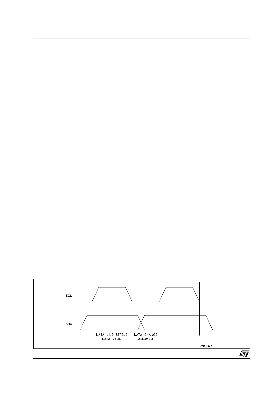
As shown in fig. 1, the data on the SDA line must be stable during the high period of the clock. The HIGH
and LOW state of the data line can only change when the c lock signal on the SCL line is LOW.
START AND STOP CONDITIONS
As s hown in fig.2 a start condition is a HIGH to LOW transition of the SDA line while SCL is HI GH. The
stop con dition is a LOW to HIGH trans ition of the SDA line while SCL is HIG H. A STOP conditions must
be sent befo re each START condition.
BYTE FORMAT
Every bytetransferred to the SDA line must contain8 bits. Ea ch byte must be followed by an acknowledge
bit. The MSB is transferred first.
ACKNOWLEDGE
The master (µP) puts a resistive HIGH level on the SDA line during the ac kn owledge clock pulse (see fig.
3). The peripheral (LNBH21) th at acknowledges has to pull-down (LOW) t he SDA line during the
acknowledge clock pulse, so that the SDA line is stable LOW during this clock pulse. The peripheralwhich
has been addressed has togenerate an acknowledge after the reception of each byte, otherwise the SDA
line remains at the HIGH level during the ninth clock pulse time. In this case the m as ter transmitter can
generate the STOP information in order to abort the transfer. The LNBH21 won't generate the
acknowledge if the V
supply is belo w the Undervoltage Loc k out threshold (6.7V ty p.).
CC
TRANSMISSION WITHOUT ACKNO WL EDGE
Avoiding to detect t he acknowled ge of the LNBH21, the µP can use a simpler transmission: simply it waits
one clock without checking the slave acknowledging, and sends the new data.
This approach of course is less prot ected from misworking and decreases the noi se immunity.
Figure1 : DATA VALIDITY ON THE I
6/20
2
CBUS
Page 7
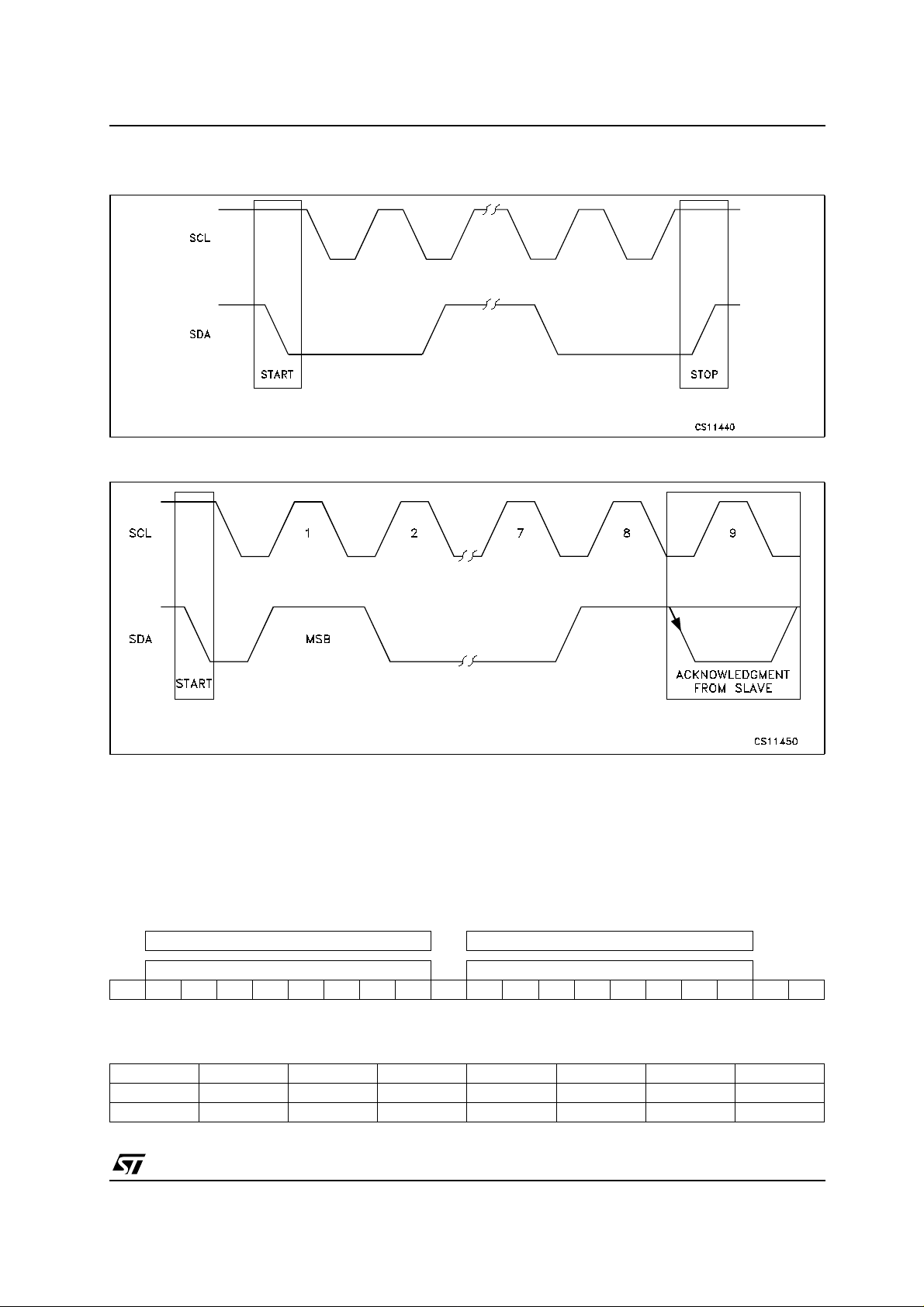
Figure2 : TIMING DIAGRAM ON I2CBUS
2
Figure3 : ACKNOWLEDGE ON I
CBUS
LNBH21
LNBH21 SOFTWARE DESC RIPTION
INTERFACE PROTOCOL
The interface protoc ol comprises:
- A start condition (S)
- A chip address byte = hex 10 / 11 (the LSB bit determines read(=1)/write(=0) transmission)
- A seque nc e of data (1 byte + acknowledge)
- A stop condition (P)
CHIP ADDRESS DATA
MSB LSB MSB LSB
S0001000R/WACK ACKP
ACK= Acknowledge; S = Start ; P = Stop; R/W = Read/Write
SYSTEM REGISTER (SR, 1 BYTE)
MSB LSB
R, W R, W R, W R, W R, W R, W R R
PCL TTX TEN LLC VSEL EN OTF OLF
R,W = read and write bit; R = Read-only bit
All bitsreset to0 at Power-On
7/20
Page 8
LNBH21
TRANSMITTED DATA (I2C BUS WRITE MODE)
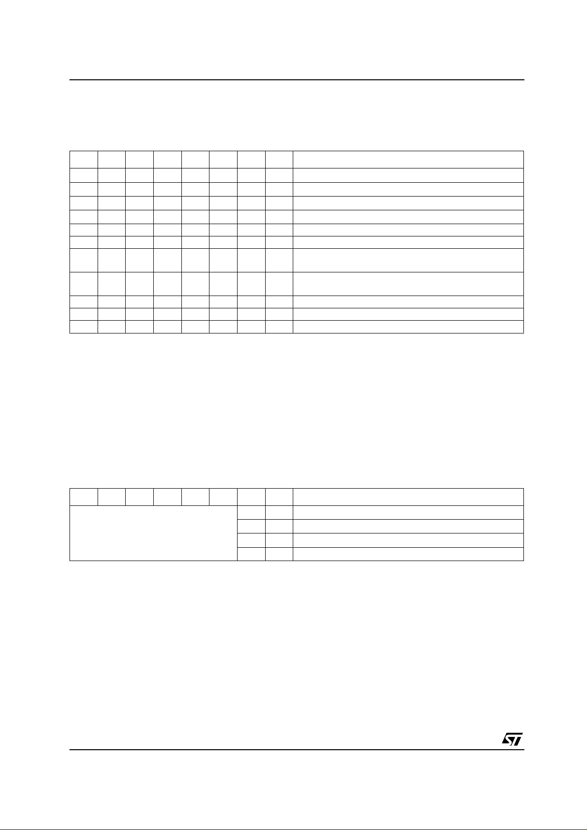
When the R/W bitin the chip addres s is set to 0,the main µP can writeon the System Register (SR)of the
LNBH21 viaI
left to the di agnos tic flags, and are read-only.
PCL TTX TEN LLC VSEL EN OTF OLF Function
0 1 X X Pulsed (dynamic) current limiting is selected
1 1 X X Static current limiting is selected
XXXXX0XXPowerblocksdisabled
X= don't care.
Values are typical unless otherwise specified
2
C bus. Only 6 bits out of the 8 available can be written by the µP, since the remaining 2 are
V
001XX
011XX
101XX
111XX
0 1 X X 22KHz is controlled by DSQIN pin
1 1 X X 22KHz tone is ON, DSQIN pin disabled
01XX
1X 1XX
=13.25V,VUP= 15.25 V
O
V
=18V,VUP=20 V
O
=14.25V,VUP= 16.25 V
V
O
=19.5V,VUP=21.5V
V
O
V
RX output is ON, output voltage controlled by VSEL and
O
LLC
V
TX output is ON, 22KHz controlled by DSQIN or TEN,
O
output voltage level controlled by VSEL and LLC
RECEIVED DATA (I2C bus READ MODE)
The LNBH21 canprovide to theMaster a copy of the SYSTEM REGISTER information viaI2C bus inread
mode. The read mode is Master activated by sending the chip address with R/W bit set to 1. At the
following master generated clocks bits, the LNBH21 issues a byte on the SDA data bus line (MSB
transmitted first).
At the ninth clock bit the MCU master can:
- acknowledge the reception, starting in this way the transmissio n of another byte from the LNBH21;
- no acknowledge, stopping the read mode communication.
While the whole register is read back by the µP, only the two read-only bits OLF and OTF convey
diagnostic informations about the LNBH21.
Values are typ ical unless otherwise specified.
PCL TTX TEN LLC VSEL EN OTF OLF Function
<140°C, normal operation
T
J
T
>150°C, power block disabled
J
0
1
I
OUT<IOMAX
I
OUT>IOMAX
, normal operation
, overload protection triggered
These bits are read exactly the same as
they were left after last write operation
Values are typical unless otherwise specified
0
1
POWER-ON I2C INTERFACE RESET
2
C interface built in the LNBH21 is automatically reset at power-on. As long as the VCCstays below
The I
the UnderVoltage Lockout threshold (6.7V typ.), the interface will not respond to any I
2
C command and
the System Register (SR) is initialized t o all zeroes, thus keeping the power block s disabled. Once the
V
rises above 7.3V typ, the I2C interface becomes operative and the SR can be configured by the main
CC
µP. This is due to 500mV of hystere sis prov ided in the UVL threshold to av oid false retriggering of the
Power-On reset circuit.
ADDRESS PIN
Connecting this pin to GND the Chip I
2
C interface address is 0001000, but, it is possible to choice among
4 different addresses simply setting this pin at 4 fixed voltage levels (see table on page 10 ).
8/20
Page 9

LNBH21
DiSEqCTM IMPLEMENTATION
The LNBH21 helps the systemdesigner to implement the bi-directional (2.0) Di SEqC proto col by allowing
an easy PWK modulation/demodulation of the 22KHz carrier. The PWK data are exchanged between the
LNBH21 and the main µP using logic levels that are compatible with both 3.3 and 5V microcontrolle rs.
This data exchange is made through two dedicated pins, DS QI N and DS QOUT, in order to maintain the
timing relationships between the PWK data and the PWK modulation as accurate as possible. These two
pins should be directly connected to two I/O pins of the µP, t hus leaving to the re sident firmware the task
of encoding and decoding the P WK data in accordance to the DiSEqC protocol. Full compliance of the
system tothe specificationis thus not implied bythe bare use of the LNBH21. The systemdesigner should
also take in consideration the bus hardware requirements; that can be simply accomplished by the R-L
termination connected on the V
4. To avoid any losses due to the R-L impedance during t he tone transmission, the LNBH21 has
dedicated output (V
TX) that, in a DiSEqC 2.0 application, is connected after the filter and mus t be
O
enabled by setting the TTX S R bit HIGH only during the tone transmission (see DiSEq C 2.O operation
description on page2).
Unidirectional (1.x) Di SEqC and n on-DiS EqC systems normall y don't need this te rmina tion, and the V
pin can be directly connected to the LNB supply port of the Tuner (see DiSeqC 1.x application circuit on
pag.4). There is also no need of Tone Decoding, thus DE TI N and DSQOUT pins can be left unconnected
and the Tone is provided by the V
pins of the LNBH21, as shown in the Typical Application Circuit on page
O
TX.
O
TX
O
9/20
Page 10
LNBH21
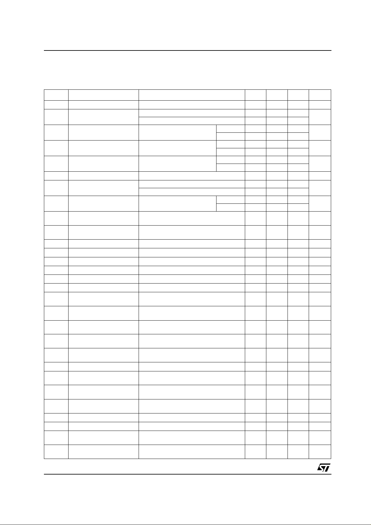
ELECTRICAL CHARACTERISTICS FO R LNBP SERIES(TJ= 0 to85°C, EN=1, TTX=0/1,DSQI N =LOW,
LLC=TEN=PCL=VSEL=0, V
section for I
Symbol Parameter Test Conditions Min. Typ. Max. Unit
V
IN
I
I
V
O
V
O
∆V
∆V
I
MAX
I
SC
t
OFF
t
ON
f
TONE
A
TONE
D
TONE
t
r,tf
G
EXTM
V
EXTM
Z
EXTM
f
SW
f
DETIN
V
DETIN
Z
DETIN
V
OL
I
OZ
V
IL
V
IH
I
IH
I
OBK
T
SHDN
∆T
SHDN
2
C access to the system register).
Supply Voltage IO= 750 mA TEN=VSEL=LLC=1 8 15 V
Supply Current EN=TEN=VSEL=LLC=1, NO LOAD 20 40 mA
Output Voltage IO= 750 mA VSEL=1 LLC=0 17.3 18 18.7 V
Output Voltage IO= 750 mA VSEL=0 LLC=0 12.75 13.25 13.75 V
Line Regulation V
O
Load Regulation VSEL=0 or 1, IO= 50 to 750mA 200 mV
O
Output Current Limiting ISEL = Floating or V > 3.3V 750 1000 mA
Output Short Circuit Current VSEL=0 300 mA
Dynamic Overload
protection OFF Time
Dynamic Overload
protection ON Time
Tone Frequency TEN=1 20 22 24 KHz
Tone Amplitude TEN=1 0.55 0.72 0.9 V
Tone Duty Cycle TEN=1 40 50 60 %
Tone Rise and Fall Time TEN=1 5 8 15 µs
External Modulation Gain ∆V
External Input Voltage AC Coupling 400 mV
External Modulation
Impedance
DC/DC ConverterSwitching
Frequency
Tone Detector Frequency
Capture Range
Tone Detector Input
Amplitude
Tone Detector Input
Impedance
DSQOUT Pin Logic LOW Tone present IOL=2mA 0.3 0.5 V
DSQOUT Pin Leakage
Current
DSQIN Input Pin Logic
LOW
DSQIN Input Pin Logic
HIGH
DSQIN Pins Input Current VIH=5V 15 µA
Output Backward Current EN=0, V
Temperature Shutdown
Threshold
Temperature Shutdown
Hysteresis
=12V, IO=50mA, unless otherwise specified. See sof tware description
IN
EN=0 3.5 7
LLC=1 18.7 19.5 20.3
LLC=1 13.75 14.25 14.75
= 8 to 15V VSEL=0 5 40 mV
IN1
VSEL=1 5 60
ISEL = GND 450 700
VSEL=1 200
PCL=0 Output Shorted 900 ms
PCL=0 Output Shorted t
OUT
/∆V
, f = 10Hz to 50KHz 6
EXTM
/10 ms
OFF
f = 10Hz to 50KHz 260 Ω
220 kHz
0.4Vpp sinewave 18 24 kHz
fIN=22kHz sinewave 0.2 1.5 V
150 kΩ
Tone absent VOH=6V 10 µA
0.8 V
2V
= 18V -6 -15 mA
OBK
150 °C
15 °C
PP
PP
PP
10/20
Page 11
LNBH21
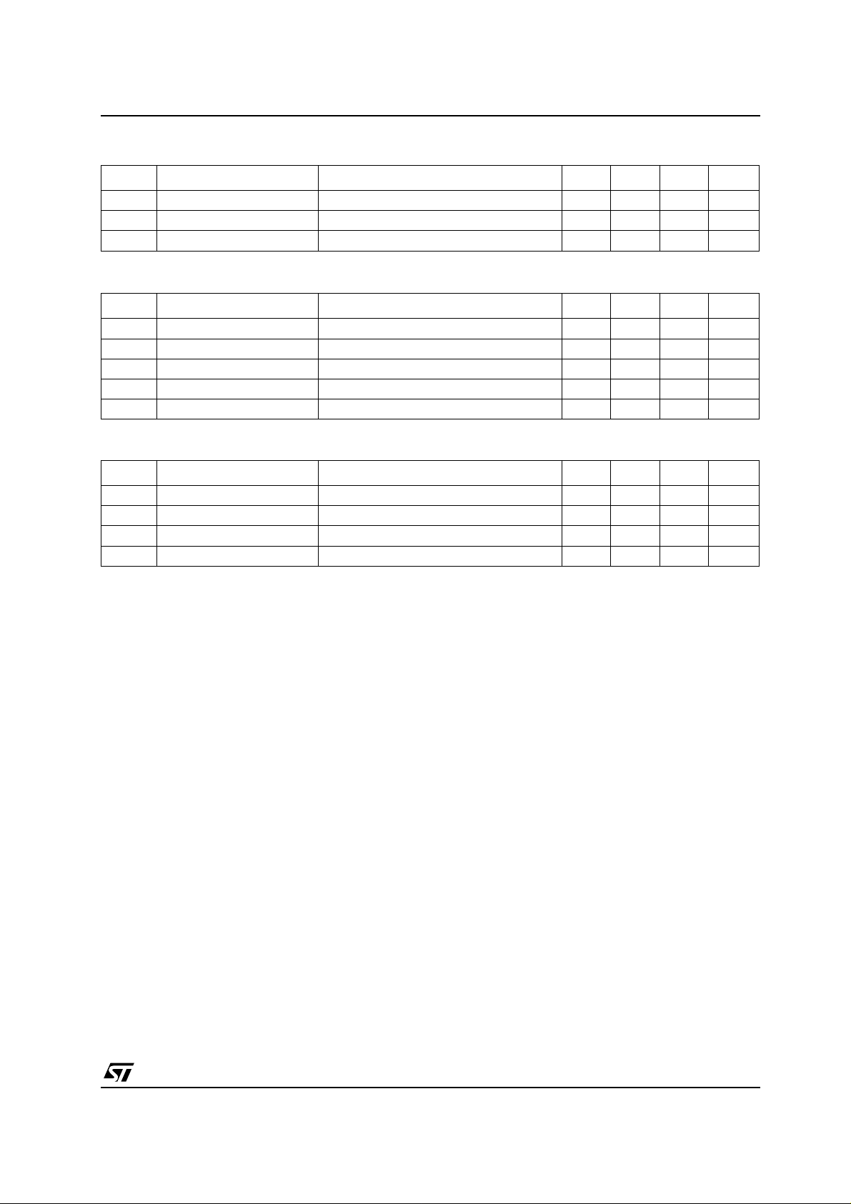
GATE AND SENSE ELECTRICA L CHARACTERISTICS (TJ= 0 to 85°C, VIN= 12V)
Symbol Parameter Test Conditions Min. Typ. Max. Unit
R
DSON-L
R
DSON-H
V
SENSE
2
C ELECTRICAL CHARACTERISTICS (TJ=0to85°C,VI= 12V)
I
Symbol Parameter Test Conditions Min. Typ. Max. Unit
f
GateLOW R
Gate HIGH R
DSON
DSON
I
= -100mA 4.5 Ω
GATE
I
= 100mA 4.5 Ω
GATE
Current Limit Sense Voltage 200 mV
V
LOW Level Input Voltage SDA, SCL 0.8 V
IL
V
HIGH Level Input Voltage SDA, SCL 2 V
IH
Input Current SDA, SCL, VI= 0.4 to 4.5V -10 10 µA
I
I
Low Level Output Voltage SDA (open drain), IOL=6mA 0.6 V
V
OL
Maximum Clock Frequency SCL 500 KHz
MAX
ADDRESS PIN CHARACTERISTICS (T
= 0 to 85°C, VIN=12V)
J
Symbol Parameter Test Conditions Min. Typ. Max. Unit
V
ADDR-1
V
ADDR-2
V
ADDR-3
V
ADDR-4
"0001000" Addr Pin Voltage 0 0.7 V
"0001001" Addr Pin Voltage 1.3 1.7 V
"0001010" Addr Pin Voltage 2.3 2.7 V
"0001011" Addr Pin Voltage 3.3 5 V
11/20
Page 12
LNBH21
THERMAL DESIGN NOTES
During normal operation, the LNBH21 dev ice dissipates some power. At maximum rated output current
(750mA), the voltage drop on the linear regulator lead to a total dissipated power that is typically 1.65W.
The heat generated requires a suitable heat sink to keep the junction temperature below the over
temperature protection threshold. Assu min g a 45°C t emperature inside the Set-Top-Box case, the total
R
While this can be easily achieved using a through-hole power package that can be attached to a small
heatsink or to the metallic frame of the rec eiver, a surface mount power package must rely on PCB
solutions whose thermal efficiency is often limited. The simplest solution is to use a l arge, continuous
copper area of the GND layer to dissipate the heat coming from th e IC body.
GivenanR
achieved if a minimum of 6.5cm
GND layer of a multi-layer PCB, or, in a dual layer P C B, an unbroken GND area even on the opposite side
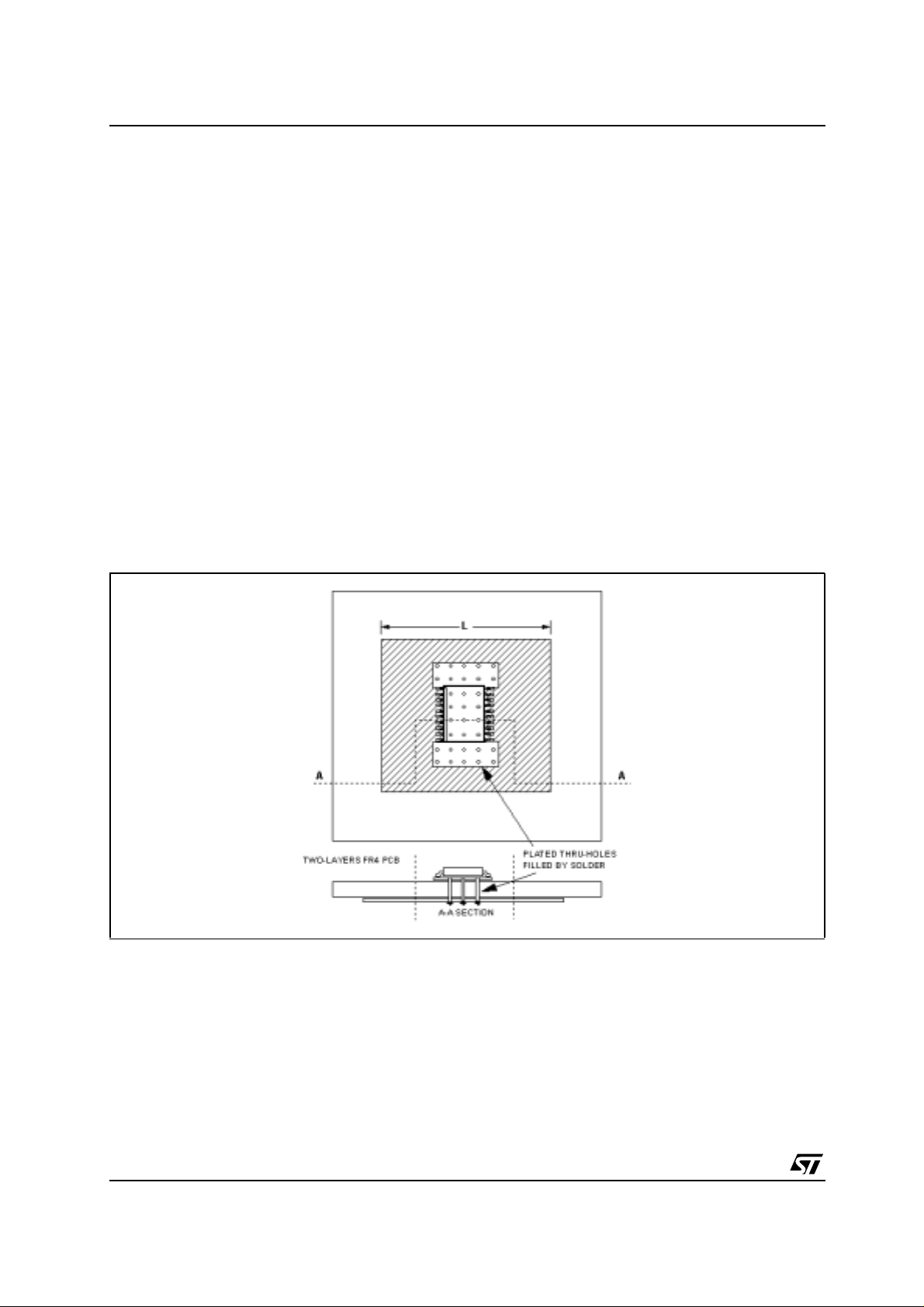
where the IC is placed. In figure 4, it is shown a suggested layout f or the PSO-20 package with a dual
layer PCB, where the IC exposed pad connected to GND and the square dissipating area are th ermally
connected through 32 vias holes, filled by solder. This a rrangement, when L=25mm, achieves an R
of about 3 2°C/W.
Different layouts are possible, too. Ba sic prin ciples, h owev er, suggest to keep the IC and its grou nd
exposed pad approximately in the middle of the dissipati ng area; to provide as many vias as poss ible; to
design a dissipating area having a shape as square as possible and not interrupted by other copper
traces.
Figure4 : PowerSO-20 SUGGESTED PCB HEATSINK LAYOUT
has to be less than 48°C/W.
thj-amb
thj-case
equal to 2°C/W, a m ax im um of 46°C/W are left to the PCB heatsink. This figure is
2
copper area is placed just below the IC body. This area can be the inner
thc-amb
12/20
Page 13
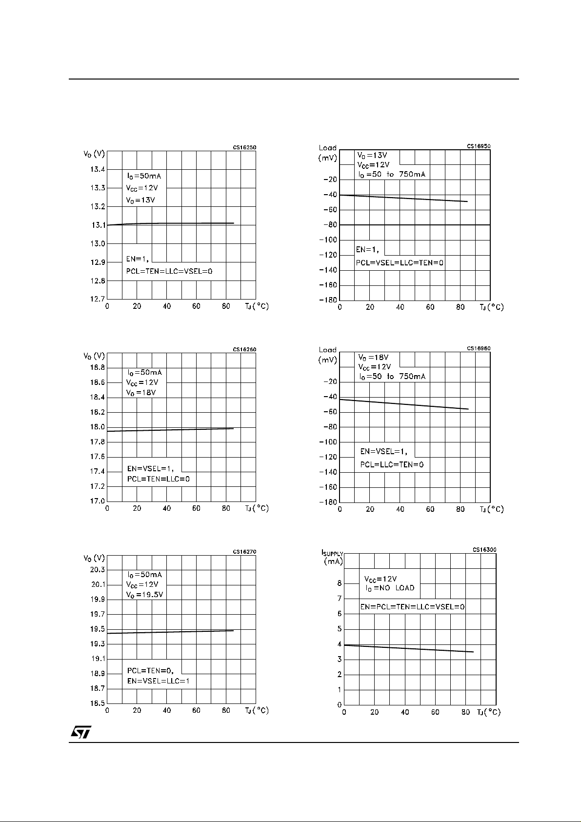
TYPICAL CHARACTERISTICS (unless otherwise spec ified Tj=25°C)
LNBH21
Figure5 : Output Voltage vs Temperature
Figure6 : Output Voltage vs Temperature
Figure8 : Load Regulation vs Temperature
Figure9 : Load Regulation vs Temperature
Figure7 : Output Voltage vs Temperature
Figure10 : Supply Current vs T emperature
13/20
Page 14
LNBH21
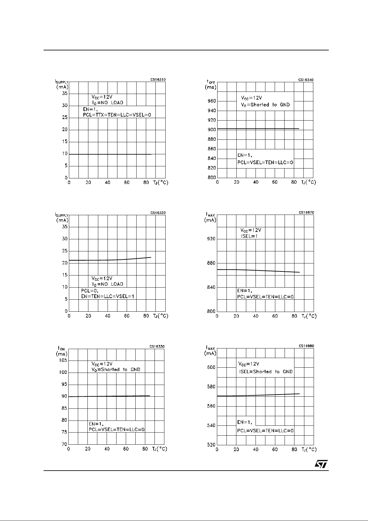
Figure11 : Supply Current vs T emperature
Figure12 : Supply Current vs T emperature
Figure14 : Dynamic Overload Protection OFF
Time vs Temperature
Figure15 : Output Current Limiting vs
Temperature
Figure13 : Dynamic Overload Protection ON
Time vs Temperature
14/20
Figure16 : Output Current Limiting vs
Temperature
Page 15
LNBH21
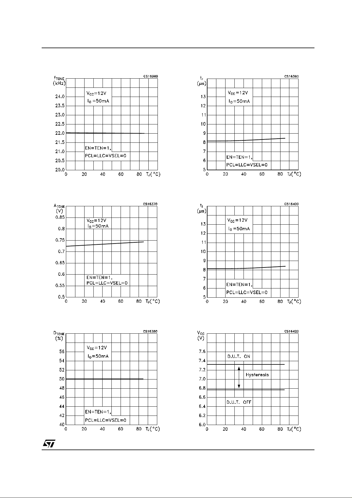
Figure17 : Tone Frequency vs Temperature
Figure18 : Tone Amplitude vs Temperature
Figure20 : Tone Rise Time vs Temperature
Figure21 : Tone Fall Time vs Temperature
Figure19 : Tone Duty Cycle vs Temperature
Figure22 : Undervoltage Lockout Thres hold vs
Temperature
15/20
Page 16
LNBH21
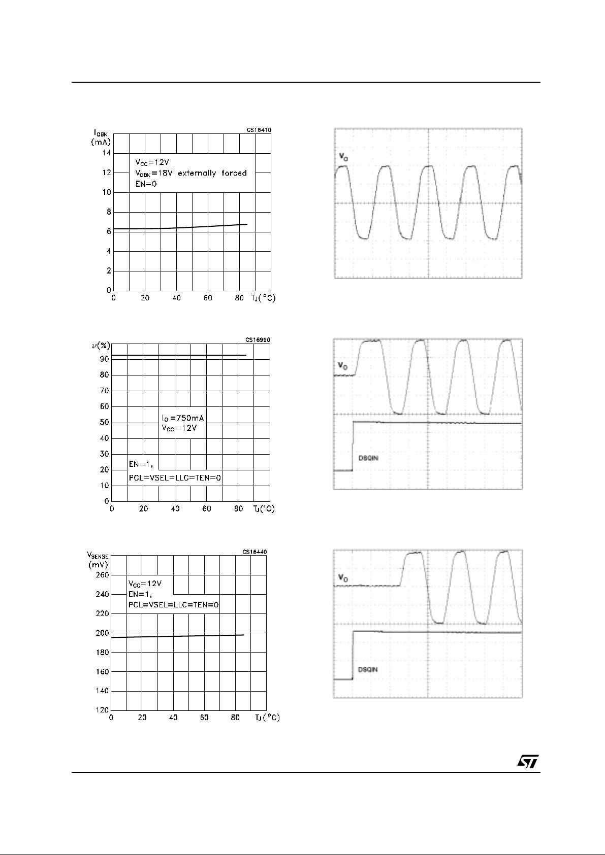
Figure23 : Output Backward Current vs
Temperature
Figure24 : DC/DC Converter Efficiency vs
Temperature
Figure26 : 22kHz Tone Waveform
VCC=12V, IO=50mA, EN=TEN=1
Figure27 : DSQIN Tone Enable Transient
Response
Figure25 : Current Limit Sense Voltage vs
Temperature
16/20
VCC=12V, IO=50mA, EN=1, Tone enabled by DSQIN Pin
Figure28 : DSQIN Tone Enable Transient
Response
VCC=12V, IO=50mA, EN=1, Tone enabled by DSQIN Pin
Page 17
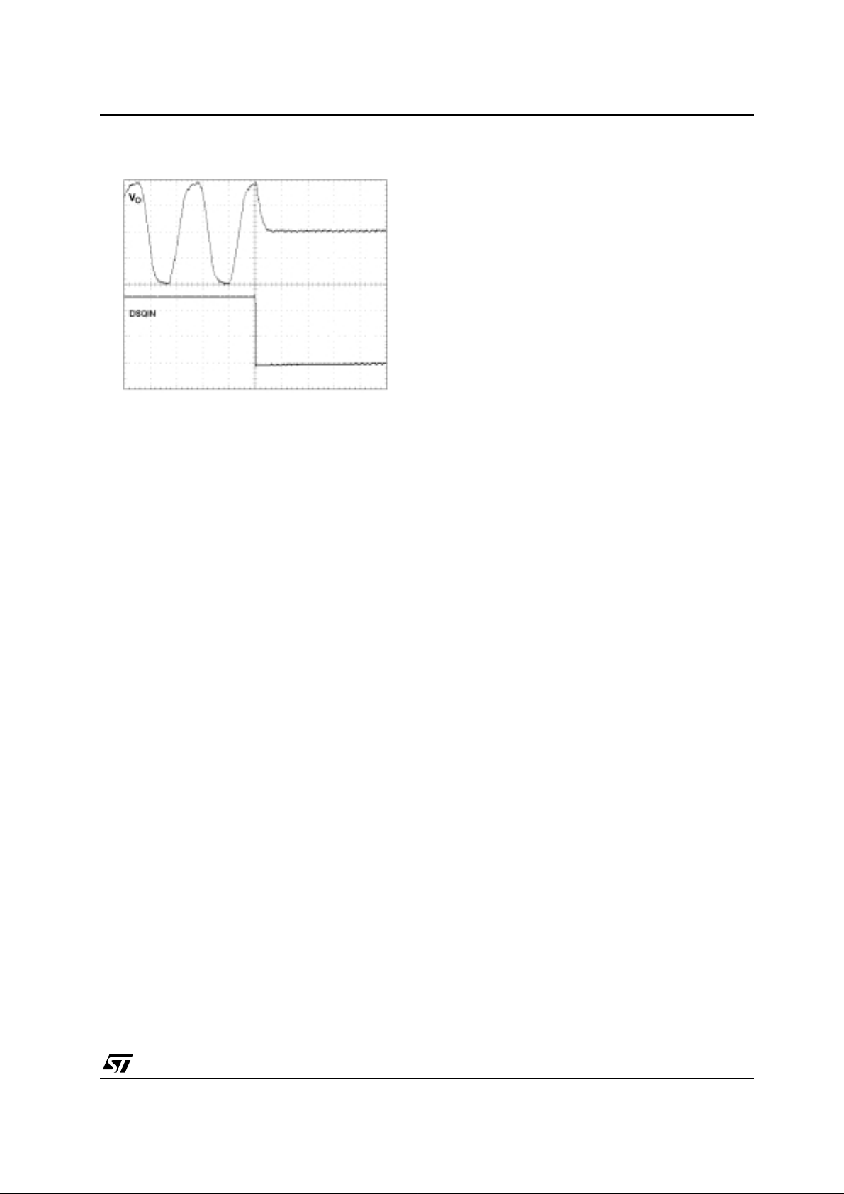
Figure29 : DSQIN Tone Disable Transient
Response
VCC=12V, IO=50mA, EN=1, Tone enabled by DSQIN Pin
LNBH21
17/20
Page 18
LNBH21
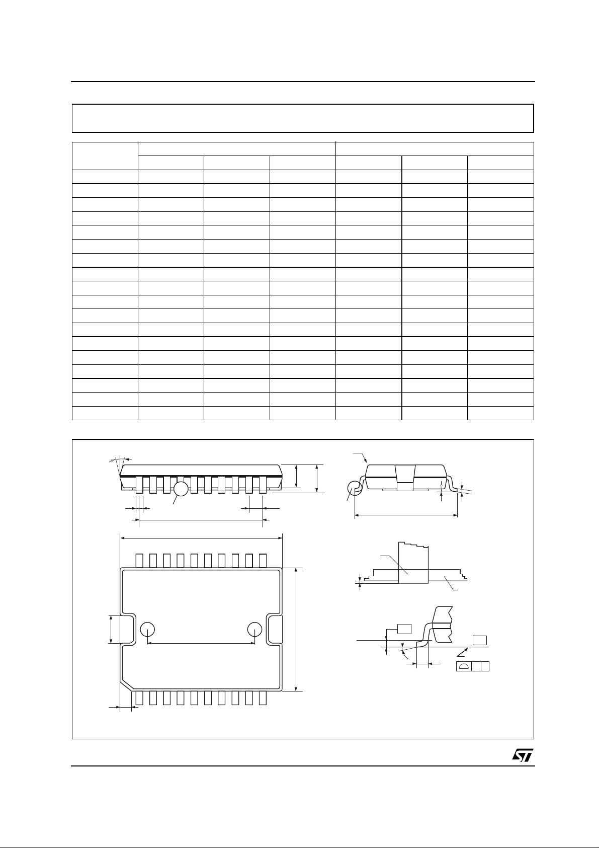
PowerSO-20 MECHANICAL DATA
DIM.
MIN. TYP MAX. MIN. TYP. MAX.
mm. inch
A 3.60 0.1417
a1 0.10 0.30 0.0039 0.0118
a2 3.30 0.1299
a3 0 0.10 0 0.0039
b 0.40 0.53 0.0157 0.0209
c 0.23 0.32 0.0090 0.0013
D (1) 15.80
16.00
0.6220 0.630
E 13.90 14.50 0.5472 0.5710
e 1.27 0.0500
e3 11.43 0.4500
E1 (1) 10.90 11.10 0.4291 0.4370
E2 2.90 0.1141
G 0 0.10 0.0000 0.0039
h 1.10 0.0433
L 0.80 1.10 0.0314 0.0433
N
0˚
1
10˚
S0˚ 8˚0˚ 8˚
T 10.0 0.3937
(1) “D and E1” do not include mo
ld flash or protusions - Mold flash or protusions shall not exceed 0.15mm (0.00
”)
6
E2
h x45˚
NN
a2
b
DETAIL A
110
e3
D
T
e
1120
A
E1
DETAIL B
PSO20MEC
R
lead
a3
Gage Plane
E
DETAIL
0.35
S
B
a1
L
c
DETAIL A
slug
-C-
SEATING PLANE
GC
(COPLANARITY)
0056635
18/20
Page 19
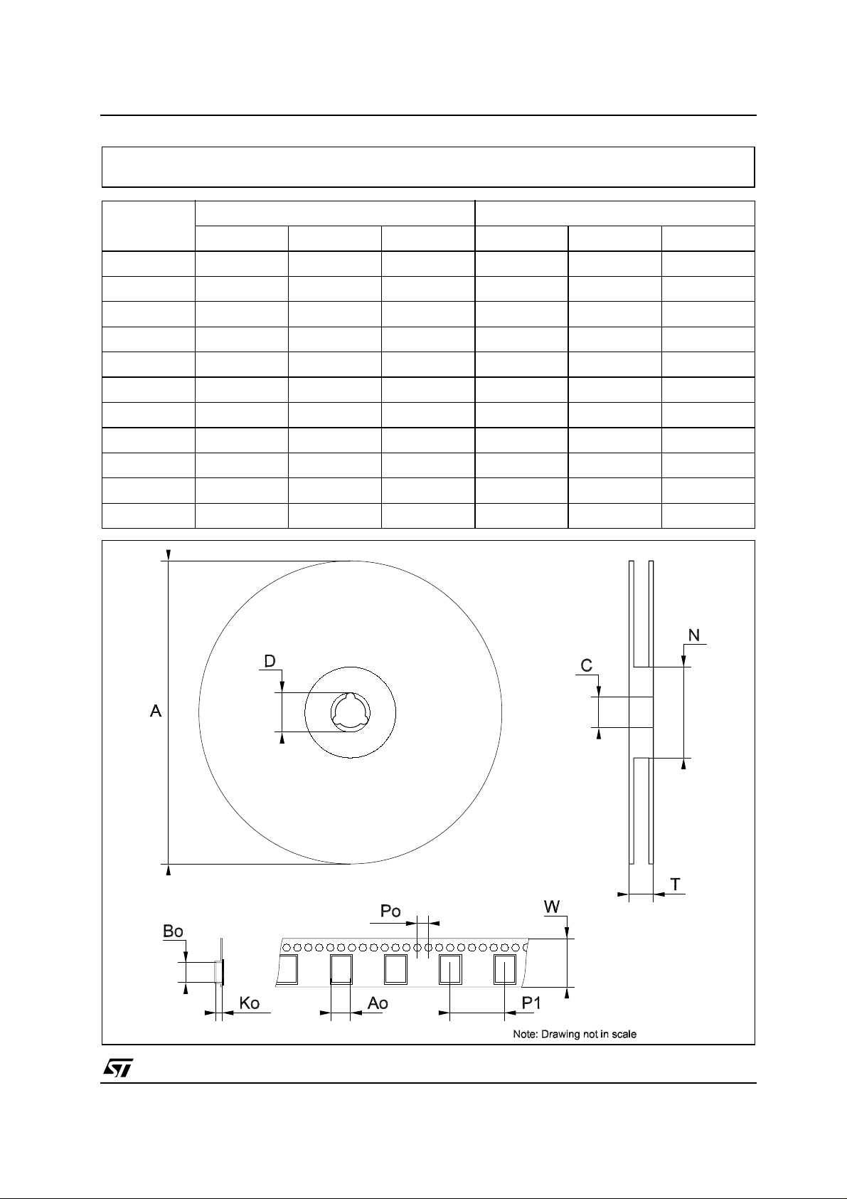
Tape & Reel PowerSO-20 MECHANICAL DATA
LNBH21
DIM.
MIN. TYP MAX. MIN. TYP. MAX.
A 330 12.992
C 12.8 13.2 0.504 0.519
D 20.2 0.795
N 60 2.362
T 30.4 1.197
Ao 15.1 15.3 0.594 0.602
Bo 16.5 16.7 0.650 0.658
Ko 3.8 4.0 0.149 0.157
Po 3.9 4.1 0.153 0.161
P 23.9 24.1 0.941 0.949
W 23.7 24.3 0.933 0.957
mm. inch
19/20
Page 20

LNBH21
Information furnished is believed to be accurate and reliable. However, STMicroelectronics assumes no responsibility for the
consequences of use of such inform ation nor fo r an y infring ement of p atents or o ther rights of third p arties which may r esult f rom
its use. No license is granted by implication or otherwise under any patent or patent rights of STMicroelectronics. Specifications
mentioned in this publication are subject to change without notice. This publication supersedes and replaces all information
previously supplied. STMicroelectronics products are not authorized for use as critical components in life support devices or
systems without express written approval of STMicroelectronics.
Australia - Belgium - Brazil - Canada - China - Czech Republic - Finland - France - Germany - Hong Kong - India - Israel - Italy - Japan -
Malaysia - Malta - Morocco - Singapore - Spain - Sweden - Switzerland - United Kingdom - United States.
The ST logo is a registered trademark of STMicroelectronics
All other names are the property of their respective owners
© 2004 STMicroelectronics - All Rights Reserved
STMicroelectronics GROUP OF COMPANIES
http://www.st.com
20/20
 Loading...