

Page 1
LMX5001
Dedicated Bluetooth Link Controller
General Description
The LMX5001 Dedicated Bluetooth™Link Controller has
been designed to interface with the LMX3162, Single Chip
Radio Transceiver to provide a rapid design path to a complete Bluetooth physical layer.
The LMX5001 also offers a low power and cost competitive
solution to the Bluetooth Link Controller function.
The LMX5001 can be attached to a Link Management Controller, or Host processor performing the Link Management
function to implement a complete Bluetooth interface.
Bluetooth is a world-wide recognized wireless communication standard, whichoperates in the ISM band (2.4 GHz), offering a low cost and convenient wireless replacement for
data/voice cable links between fixed and mobile electronic
devices.
Utilizing a GFSK modulation scheme, with frequency hopping, Bluetooth is able to offer a low power, low cost, robust
and spectrally efficient spread spectrum packet data system.
Features
n Bluetooth Specification 1.0B compliant
n Bluetooth physical layer, available today
n Supports Class 1, 2 and 3 Bluetooth (20 dBm, 4 dBm
and 0 dBm links)
n 1/8 bit sampling resolution
n Power management for Tx, Rx and PLL
n Piconet and Scatternet communication capable
n Good Bluetooth radio range coverage (when coupled
with the LMX3162)
n Support for RSSI channel quality monitoring
n Bluetooth Encryption Engine
Applications
n PCMCIA Cards
n Mobile Phones
n Laptop PCs
n Palmtop PCs
n Desktop PCs
n Computer Peripherals
n Wireless Modems
n PDAs
n Palmtops
n P.O.T.S
n Digital Cameras
n Fax
n Printers
n Bar-code Readers
n Notepads
n Cordless Headsets
n In-vehicle Communications
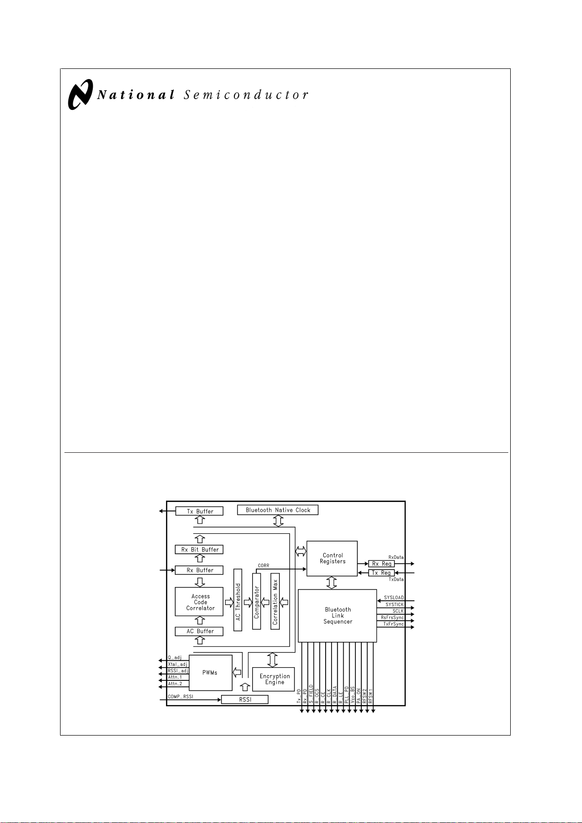
Block Diagram
Functional Block Diagram
DS101340-1
PRELIMINARY
April 2000
LMX5001 Dedicated Bluetooth Link Controller
© 2000 National Semiconductor Corporation DS101340 www.national.com
Page 2
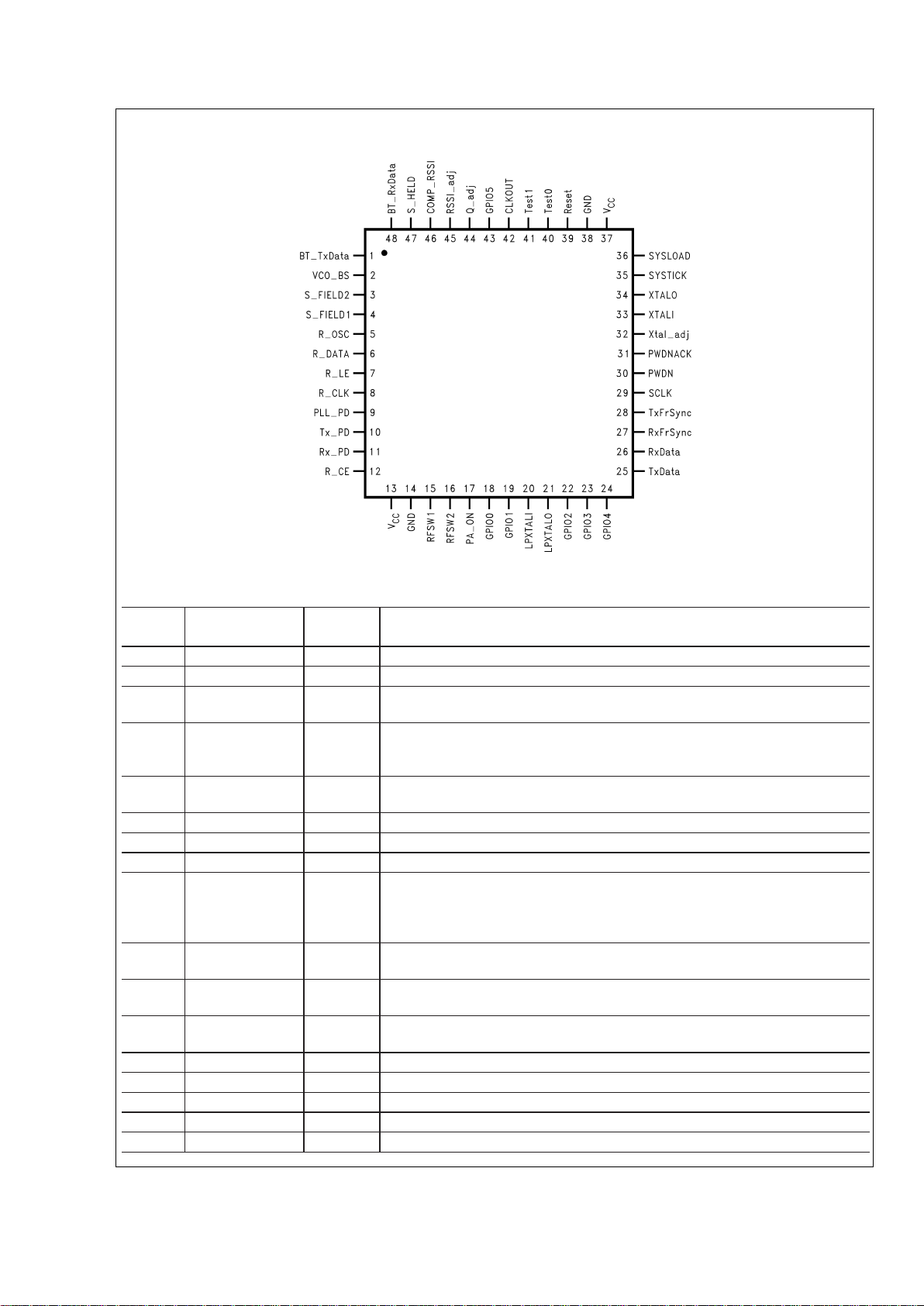
Connection Diagram
Pin Descriptions
Pin
No.
Pin Name I/O Description
1 BT_TxData O Transmit data
2 VCO_BS O VCO band switch control signal.
3 S_FIELD2 O LMX3162 DC compensation circuit enable. This signal is enabled (low) throughout
the correlation phase.
4 S_FIELD1 O LMX3162 DC compensation circuit enable. At the beginning of the correlation
phase this signal is enabled (low) for 15 µs. For the remainder of the correlation
phase this signal is PWM by 1/8 (cycle time = 1 µs).
5 R_OSC O LMX3162 4 MHz oscillator input to the PLL synthesizer. This signal is only
enabled when the LMX3162 is active.
6 R_DATA O MICROWIRE
™
data to LMX3162.
7 R_LE O MICROWIRE load enable to LMX3162.
8 R_CLK O MICROWIRE clock to LMX3162.
9 PLL_PD O LMX3162 PLL power down. This signal is used to open the PLL loop or powering
down the PLL. The PLL loop is opened when transmitting to make it possible to
FSK modulate the VCO. When receiving it is optional to open the PLL loop
(configured by the PLLOpenRX bit in threshold_msb).
10 Tx_PD O LMX3162 Transmitter power down. For power conservation, the Transmitter is
only powered during Transmit Frames.
11 Rx_PD O LMX3162 Receiver power down. For power conservation, the Receiver is only
powered during Receive Frames.
12 R_CE O LMX3162 chip enable. When the LMX5001 is in Idle Mode the LMX3162 is
powered down.
13 V
CC
Power +3.3V
14 GND Power 0V
15 RFSW1 O Antenna switch control.
16 RFSW2 O Antenna switch control. This signal is RFSW1 inverted,
17 PA_ON O Switches the external PA on/off for 20 dBm/0 dBm transmission, respectively.
DS101340-7
LMX5001
www.national.com 2
Page 3

Pin Descriptions (Continued)
Pin
No.
Pin Name I/O Description
18 GPIO0
(XTAL Config)
I/O XTAL configuration during reset (Note 1).
19 GPIO1
(XTAL Config)
I/O XTAL configuration during reset (Note 1).
20 LPXTALI I 128 kHz XTAL connection for low power mode. This is used in low power mode. If
the low power mode is not used it is not necessary with at XTAL here. External
128 kHz clock can also be feed in here.
21 LPXTALO O 128 kHz XTAL connection.
22 GPIO2 I/O General Purpose I/O
23 GPIO3 I/O General Purpose I/O
24 GPIO4 I/O General Purpose I/O
25 TxData I LCI Data Transmit
26 RxData O LCI Data Receive
27 RxFrSync O LCI Receive Frame Sync.
28 TrFrSync O LCI Transmit Frame Sync.
29 SCLK O LCI Serial Clock.
30 PWDN O Power Down to Link Management Controller
31 PWDNACK I Power Down Acknowledge from Link Management Controller
32 Xtal_adj O PWM signal to make adjustments to the XTAL.
33 XTALI I 16 MHz XTAL connection. (External clock input).
34 XTALO O 16 MHz XTAL connection.
35 SYSTICK O Systick generated from the internal LMX5001 Master/Slave Counter.
36 SYSLOAD I When low holds the LMX5001 in Idle Mode. A rising edge causes a system load
After a rising edge the LMX5001 will start to load control data from and store
status information to the LMC via the LCI.
37 V
CC
Power
38 GND Power
39 Reset I Reset. After Reset is released the LMX5001 will be in Idle Mode, awaiting a
SYSLOAD.
40 Test0 I Should be tied low. This signal is used in production test.
41 Test1 I Should be lied low. This signal is used in production test.
42 CLKOUT O Xtal clock output to Link Management Controller. This signal can be disabled
using the Sysload Command (for power saving).
43 GPIO5 I/O General Purpose I/O
44 Q_adj O PWM signal to make it possible to adjust the quadrature tank circuit to the
LMX3162.
45 RSSI_adj O PWM signal for use in creating an RSSI AD converter.
46 COMP_RSSI I Output from the external comparator in the RSSI AD converter.
47 S_Field3 O DC Compensation circuit enable. At the beginning of the correlation phase, this
signal is enabled (low) for 15 µs.
48 BT_RxData I Receive data.
Note 1: During Reset GPIO0 and GPIO1aresampledto setup the Xtal division ratio. The assumed external Xtal frequency is derived using the following relationship:
GPIO1 GPIO0 Xtal Division Ratio
Low Low Divide by 2 (i.e., 16 MHz XTAL or clock input).
Low High Divide by 3 (i.e., 24 MHz XTAL or clock input).
High Low Divide by 4 (i.e., 32 MHz XTAL or clock input).
High High Not used.
After Reset is completed, GPIO0 and GPIO1 can be used as normal general purpose I/Os.
LMX5001
www.national.com3
Page 4
Absolute Maximum Ratings (Note 2)
If Military/Aerospace specified devices are required,
please contact the National Semiconductor Sales Office/
Distributors for availability and specifications.
Operating Ambient Temperature 0˚C to +70˚C
Storage Temperature −65˚C to +150˚C
Maximum Input Voltage:
Inputs V
DD
+0.5V
5V Tolerant V
DD5
+0.5V
Maximum Operating Voltage 3.6V
Note 2: Stresses beyond those listed under “Absolute Maximum Ratings”
may cause permanent damage to the device. This is a stress rating only and
functional operation of the device at these or any other conditions beyond
those indicated in the operational sections of this specification is not implied.
Exposure to absolute maximum rating conditions for extended periods may
affect device reliability.
DC Electrical Characteristics
Symbol Parameter Conditions Min Typ Max Units
T
A
Ambient Temperature 0 70 ˚C
V
DD
Supply Voltage 3.0 3.3 3.6 V
I
IH
High-Level Input Current VIN=VDD;VDD=V
DDmax
10 µA
I
IL
Low-Level Input Current VIN=VSS;VDD=V
DDmax
, −10 µA
I
OZ
High-Impedance State Output
Current
VIN=VDDor VSS,VDD=V
DDmax
,
−10 10
µA
I
OC
Output Short-Circuit Current
This is true for all outputs
except crystal outputs XTALO
and LPXTALO.
V
OUT=VDD;VDD=VDDmax
70
mA
V
OUT=VSS;VDD=VDDmax
−45
V
IH
High-Level Input Voltage 2.0 1.7 V
V
IL
Low-Level Input Voltage 1.1 0.8 V
V
OH
High-Level Output Voltage IOH= As rated; VDD=V
DDmin
all outputs except XTALO and
LPXTALO are rated with IOH = 10ma
and IOL = -10mA. XTALO is rated
+/-8mA and LPXTALO is rated +/-2mA.
0.7 V
DD
V
V
OL
Low-Level Output Voltage IOL= As rated; VDD=V
DDmin
all outputs except XTALO and
LPXTALO are rated with IOH = 10ma
and IOL = -10mA. XTALO is rated
+/-8mA and LPXTALO is rated +/-2mA.
0.4 V
Functional Description
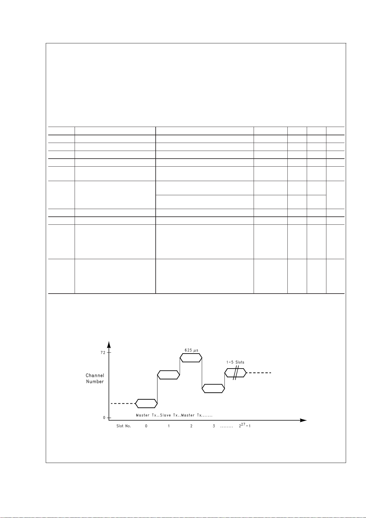
BLUETOOTH COMMUNICATION
The following illustrates a Bluetooth, Frequency Hopping, TDD, Packet based communication link:
The LMX5001 performs all the necessary functions and interconnect to permit the LMX3162 to be operated as a Blue-
DS101340-2
FIGURE 1. Bluetooth Frequency Hopping TDD
LMX5001
www.national.com 4
Page 5

Functional Description (Continued)
tooth radio. It also provides the following functions (under the
control of either a Link Management Controller, or a Host
processor performing Link Management Control functions):
•
Receive Data and Clock recovery
•
Access Code correlation
•
Frame/Slot Counters
•
Radio control (LMX3162)
•
Radio Signal Strength Indication (RSSI)
•
DC Offset compensation
•
Data transmission and receiving
•
Link Management Controller communication (LCI)
•
Power management
•
Encryption
LMX5001 COMMAND SET
In order to support the range of Bluetooth communication
modes, the LMX5001 has the ability to implement the following commands from the Link Management Controller:
•
Slave Receive with Continuous Correlation
•
Slave Receive with Windowed Correlation
•
Slave Transmit
•
Master Receive
•
Master Transmit
•
Change to Master Clock
•
Change to Slave Clock
•
Power Down
•
Slave Receive with Windowed Correlation, Encryption
Enabled
•
Slave Transmit, Encryption Enabled
•
Master Receive, Encryption Enabled
•
Master Transmit, Encryption Enabled
The LMX5001 can also be placed into an Idle State by the
Link Management Controller asserting SYSLOAD. SYSLOAD also start the system load process. During this process, the transfer of information between LMX5001 Link
Controller and the Link Management Controller takes place.
The interface between the two is Link Controller Interface
(LCI). The formatting of the Command Set, along with Configuration and Status data, sent via the LCI is further detailed
in the LCI sections of this Datasheet.
RECEIVE DATA AND CLOCK RECOVERY
Since Bluetooth is based on a packetized, wireless communications protocol, it is necessary to frame timing from the received packets, before the data itself can be recovered. Also,
since Bluetooth supports both point-to-point and point-tomultipoint connection, it is also necessary to establish
whether the received packet is addressed to the unit in question.
In receive mode, the LMX5001 receives samples from the
LMX3162 at 8 times the Bluetooth Symbol rate (i.e., 8
Mbps). This ensures a +/- 1/8 bit accuracy for receive data
and frame/slot clocking. If the unit in question is operating as
a Slave, then the Slave (Frame/Slot) Counter is updated using the recovered frame/slot clock upon successful Access
Code correlation.
The received samples are shifted into a 512 sample Buffer in
the correlator. The length of this buffer is fixed to enable the
correlation of a 64-bit Sync Word (8x oversampled) of the
Access Code.
DATA TRANSMISSION AND RECEIVING
Bluetooth data is transferred via a serial interface (LCI) with
the Link Management Controller.The transferred data is broken down to 8-bit packets. The LCI then uses a 10-bit package to send each of these 8-bit packets using a big-endian
mode.
The big-endian mode is illustrated in the
Figure 2
below:
ACCESS CODE CORRELATION
Access Code Correlation is performed to establish whether a
packet’s payload is intended for the unit in question.
The Access Code to be correlated against the incoming Receive Data is passed to the LMX5001 from the Link Management Controller via the LCI. It is then stored in a 64-bit AC
Buffer in the LMX5001.
The AC Buffer is then correlated with the incoming Receive
Data (stored in the RX Buffer) and the maximum correlation
achieved is transferred to the Correlation Max Buffer.
The Correlation Max is then compared with the contents of
the AC (Access Code) Threshold Buffer, to determine
whether the incoming Access Code sufficiently matches the
unit in question. If the Correlation Max exceeds the AC
Threshold, then the Control Registers “CORR” flag is
cleared, to indicate a correlation.
EXTERNAL CRYSTALS
There are two external crystals, one running at 16 MHz
(
±
10 ppm) and the other at 128 kHz (±125 ppm). The higher
rate crystal is used to drive the Bluetooth native clock in normal mode. This clock is also used as the Link Management
Controller clock input. The lower rate crystal is used when
the Bluetooth unit is in low power mode. In this mode, the
higher rate crystal is shut down so is the Link Management
Controller. Leaving only the lower rate crystal running to update the internal Bluetooth native clock.
FRAME/SLOT COUNTERS
The LMX5001 maintains an internal counter. It is 28 bits in
length, to support the Bluetooth requirement for 2
27
-1 slots.
The Bluetooth slot number is generated based on this
counter. It is also the basis for the Link Management firmware to update its implementation of the Bluetooth Master
and Slave Counters. This clock is in half Bluetooth slot intervals (312.5 µs).
LMX5001 LINK CONTROLLER INTERFACE (LCI)
All Host/Link Management Control of the LMX5001 (and
LMX3162) takes place via the serial LCI.
The signals associated with this port are:
•
SYSLOAD
•
SYSTICK
DS101340-3
FIGURE 2. Big-endian Data Convention
LMX5001
www.national.com5
Page 6

Functional Description (Continued)
•
SCLK
•
TxDATA
•
RxDATA
•
RxFrSync
•
TxFrSync
The LMX5001 functions as a master when communicating
with the Bluetooth Link Management Controller/Host processor. It achieves this by providing LCI Frame (TxFrSync and
RxFrSync) and Data (SCLK) synchronization signals to the
Link Management Controller.
SYSTICK provides the Link Management Controller with
Bluetooth Frame/Slot boundary information. The SYSTICK
pauses needs a minimum width of 100 ns and are spaced at
half Bluetooth slot. Twoof those SYSTICK pauses make one
Bluetooth Frame/Slot. SYSTICK is also an indication of the
beginning of Bluetooth packets.
System Load on this LCI port occurs during Bluetooth
“Guard Space” intervals (i.e., during Frequency Hopping
transitions between two transmit/receive transactions) Reference
Figure 3
below:
IDLE MODE
When SYSLOAD is asserted by the Link Manager Controller,
the LMX5001 internal BT Link is reset and the LMX5001 is
placed in “Idle” Mode. In order to guarantee this state is
achieved SYSLOAD pause must be held for a minimum period of 2 µs.
In Idle Mode the LMX5001 will place the LMX3162 in a low
power state, and will cease processing Bluetooth Transmit
and Receive data. It will remain in this state for approximately 2 µs before “System Load” takes place.
SYSTEM LOAD
System load (Sysload) takes place between the LMX5001
and the Link Management Controller on the LCI.
Sysload will cause the LMX5001 to read commands/
configuration information and write status information from/to
the Link Management Controller via the LCI. Sysload is performed in fully duplex, synchronous mode. The complete
command and status information is sent in one synchronous
packet.
LMX5001/LMX3162 Configuration Data Transfer
LMX5001/LMX3162 Configuration Data is transmitted by the
Link Management Controller via TxData (under the control of
SCLK and TxFrameSync) on the LCI.
Configuration Data is sent as a series of bytes where Bytes
0, 10 through 17 contain LMX5001 configuration information,
Bytes 1 through 9 contain LMX3162 programming information (reference LMX3162 Datasheet for further details) and
Bytes 18 through 25 contain the Bluetooth Access Code
(employed by the LMX5001).
The data transfer relative to each Byte is detailed in
Table 1
.
TABLE 1. Configuration Data Bytes
Byte No. Bit 7 Bit 6 Bit 5 Bit 4 Bit 3 Bit 2 Bit 1 Bit 0
Byte 0 Command Code
Byte 1 PW1(19) PW1(18) PW1(17) PW1(16) PW1(15) PW1(14) PW1(13) PW1(12)
Byte 2 PW1(11) PW1(10) PW1(9) PW1(8) PW1(7) PW1(6) PW1(5) PW1(4)
Byte 3 PW1(3) PW1(2) PW1(1) PW1(0) 0000
Byte 4 PW2(19) PW2(18) PW2(17) PW2(16) PW2(15) PW2(14) PW2(13) PW2(12)
Byte 5 PW2(11) PW2(10) PW2(9) PW2(8) PW2(7) PW2(6) PW2(5) PW2(4)
Byte 6 PW2(3) PW2(2) PW2(1) PW2(0) 0000
Byte 7 PW3(19) PW3(18) PW3(17) PW3(16) PW3(15) PW3(14) PW3(13) PW3(12)
DS101340-4
Tx = Bluetooth transmit data
Rx = Bluetooth receive data
I = Idle mode
R = Read command and register information from Link Management Controller (26 Bytes)
W = Write status information to Link Management Controller (12 Bytes)
SYSLOAD = Input pin on Link Controller
FIGURE 3. LCI Communication Scheduling
LMX5001
www.national.com 6
Page 7

Functional Description (Continued)
TABLE 1. Configuration Data Bytes (Continued)
Byte No. Bit 7 Bit 6 Bit 5 Bit 4 Bit 3 Bit 2 Bit 1 Bit 0
Byte 8 PW3(11) PW3(10) PW3(9) PW3(8) PW3(7) PW3(6) PW3(5) PW3(4)
Byte 9 PW3(3) PW3(2) PW3(1) PW3(0) 0000
Byte 10 LSB of Transmit Bits
Byte 11 MSB of Transmit Bits
Byte 12 LSB of Correlation Threshold
Byte 13 RXattn RXpol TXpol PLLOpenRX RSSI_PH O MSB Corr. Thres.
Byte 14 Xtaladj PWM Value
Byte 15 Quad. PWM Value
Byte 16 GPIO5 GPIO4 GPIO3 GPIO2 CLKDIV GPIO1 GPIO0
Byte 17 _EN _EN _EN _EN 0 0 _EN _EN
Byte 18 AC(63) AC(62) AC(61) AC(60) AC(59) AC(58) AC(57) AC(56)
Byte 19 AC(55) through to AC(48)
Byte 20 AC(47) through to AC(40)
Byte 21 AC(39) through to AC(32)
Byte 22 AC(31) through to AC(24)
Byte 23 AC(23) through to AC(16)
Byte 24 AC(15) through to AC(8)
Byte 25 AC(7) through to AC(0)
LMX5001 CONTROL DATA—Byte 0
Byte 0 contains control data (reference
Table 1
) to support
Bluetooth HCI Commands by instructing the Bluetooth Link
Sequencer to perform one of the tasks listed in
Table 2
be-
low:
TABLE 2. Bluetooth Link Sequencer —Command Codes
Command
Command
Code
Slave Receive with Continuous Correlation
Upon successful correlation, native clock is updated.
0x01
Slave Receive with Windowed Correlation
Same as command Code 0x01 except that correlation window falls within 10 µs before and 78 µs after
the next SYSTICK.
0x02
Slave Transmit 0x03
Change to Master Clock
Master clock in effect the next SYSTICK.
0x04
Master Receive 0x05
Master Transmit 0x06
Change to Slave Clock
Same as Command Code 0x04 except that the Link Management Controller may update the native clock
with bits set via the “transmit bits” field.
0x07
Power Down
During power down mode, the high crystal, CLKOUT, as well as RFFE are turned off. Native clock is
updated using the low crystal. It wake at “mark” time given via the “transmit bits” field.
0x08
Slave Receive with Windowed Correlation with Encryption 0x12
Slave transmit with Encryption 0x13
Master Receive with Encryption 0x15
Master transmit with Encryption 0x16
LMX5001
www.national.com7
Page 8

Functional Description (Continued)
CONFIGURATION DATA—Bytes 1 through 9
Bytes 1 through 9 are used to transport LMX3162 Program
Words (PW), via the LMX5001. The LMX3162 is controlled
using 3 Program Words (PW1–PW3), each word being 20
bits long. Detailed information on the content and application
of these Programming Words is provided in the LMX3162
Datasheet.
CONFIGURATION DATA—Bytes 10 and 11
Bytes 10 and 11 contain “transmit bits”. It indicates number
of bits to be transferred when the command in Byte 0 signal
a transmission. This value is 12-bit in length with Byte 10
containing the least significant byte and the lower 4 bits of
Byte 11 containing the remaining 4 most significant bits (reference
Table 1
). In the “power down” command, the “transmit bits” field contains wake up point. When the lower 12 bits
of the native clock reaches this point, the Bluetooth unit
comes out of the “power down” mode and wakes up to full
power mode. The LMX5001 and LMX3162 take 3 SYSTICKs
to complete a full power up sequence.
Bit 4 of Byte 11 is used as “loadclk”. It is valid only for
“Change to Slave Clock” command. When this bit is set to 1,
the lower 12 bits of the native clock is updated with the value
in the “transmit bits” field. When this bit is 0, the native clock
remains unchanged.
CONFIGURATION DATA—Bytes 12 and 13
Bytes 12 and 13 contain a “Threshold” value. This value is
used by the LMX5001 to test for an acceptable level of correlation between the internal Bluetooth Access Code (reference Bluetooth Specification) and the Access Code from the
incoming packet. If the resulting maximum correlation exceeds this “Threshold” value then the LMX5001 achieves a
correlation. The “Correlation” Flag is set in the packet’s payload, and subsequently transferred to the Link Management
Controller (reference section on LCI Rx Data).
The Access Code Correlation Threshold is 10 bits in length
with Byte 12 containing the least significant byte of the correlation threshold and the lower 2 bits of Byte 13 containing the
remaining 2 most significant bits (reference
Table 1
).
Bits 7, 6, and 5 of Byte 13 are used for Receive Attenuation
and Receive/Transmit Polarity (reference
Table 1
). When Bit
7 is set, the RX/TX switch in Radio Frequency Front End
(RFFE) is set in the TX direction when receiving, which gives
∼20 db attenuation in the receiver to help resolving the intermodulation problem. When Bit 6 is set, the polarity of RX
data is inverted. When Bit 5 is set, the polarity of TX data is
inverted.
Bit 4 of Byte 13 is PLLOpenRX. It controls PLL loop when receiving. The loop is opened if this bit set to 1.
Bit 3 of Byte 13 is RSSI_PH. It controls RSSI value A/D conversion scheme. If it is set to 1 the conversion uses peakhold and the conversion is running throughout the entire receive phase. If it is set to 0 the conversion is running only
during the correlation phase.
CONFIGURATION DATA—Bytes 14 and 15
Bytes 14 and 15 are assigned to the control of external
modulation components (reference
Table 1
).
CONFIGURATION DATA—Bytes 16 and 17
Bytes 16 and 17 are assigned GPIO operation (reference
Table 1
). Byte 16 is used for GPIO output and Byte 17 is
used for enable and disable. When the corresponding bit in
Byte 17 is set to 0, the GPIO is input, otherwise, it is output.
Bit 3 of Byte 16 has a special meaning. When it is 1, GPIO2
(Bit 4 of Byte 16) outputs a 4 MHz clock. When it is 0, GPIO2
performs regular GPIO function.
CONFIGURATION DATA—Bytes 18 through 25
Bytes 18 through 25 contain the appropriate Sync Word part
of the access code. The Sync Word is a 64-bit value (reference
Table 1
).
LMX5001/LMX3162 STATUS DATA TRANSFER
LMX5001 (and LMX3162) status is communicated to the
Link Management Controller by use of the RxData line on
the LCI (supported by RxFrSync and SCLK signals). This
transfer is under the control of the LMX5001, and occurs at
a specific interval (reference
Figure 3
—LCI Communication
Scheduling).
Note that the Status information which is presented to the
Link Management Controller (via the LCI) details the Status
of the LMX5001 and LMX3162 for the Frame/Slot immediately prior to the current one - there is a one frame delay in
the transfer of Status information.
The data transfer relative to each Byte is detailed in
Table 3
below.
TABLE 3. Status Data Bytes
Byte No. Bit 7 Bit 6 Bit 5 Bit 4 Bit 3 Bit 2 Bit 1 Bit 0
Byte 0 Version Major Version Minor
Byte 1 GPIO5 GPIO4 GPIO3 GPIO2 0 0 GPIO1 GPIO0
Byte 2 LSB Maximum Correlation
Byte 3 000000MSBMaxCorr.
Byte 4 LSB Timescew
Byte 5 0000 MSBTimescew
Byte 6 NC(7) NC(6) NC(5) NC(4) NC(3) NC(2) NC(1) NC(0)
Byte 7 NC(15) NC(14) NC(13) NC(12) NC(11) NC(10) NC(9) NC(8)
Byte 8 NC(23) NC(22) NC(21) NC(20) NC(19) NC(18) NC(17) NC(16)
Byte 9 0000NC(27) NC(26) NC(25) NC(24)
Byte 10 0 0 0 AD value
Byte 11 reserved 0100
LMX5001
www.national.com 8
Page 9

Functional Description (Continued)
STATUS DATA— Byte 0
Bytes 0 contains LMX5001 version number. It is in
<
Major>.<Minor>format.
STATUS DATA— Byte 1
Bytes 1 contains GPIO input value. There are no corresponding enable bits for these GPIOs.
STATUS DATA— Byte 2 and 3
Bytes 2 and 3 contain maximum correlation value of the receiving package. This value is 10-bit in length with Byte 2
containing the least significant byte and the lower 2 bits of
Byte 3 containing the remaining 2 most significant bits (reference
Table 3
).
STATUS DATA— Byte 4 and 5
Bytes 4 and 5 contain timeskew value. A timeskew is the
phase difference between master and slave clock. The following formula is used to calculate timeskew: timeskew =
slave clock - master clock.
Timeskewis within the range of −2499 to 2499. Its value is in
125 ns. That represents a clock value ranging −312.5 µs to
312.5 µs.
Timeskew is 13-bit in length with Byte 4 containing the least
significant byte and the lower 5 bits of Byte 5 containing the
remaining 5 most significant bits (reference
Table 3
).
STATUS DATA— Byte 6 through 9
Bytes 6 through 9 contain the value of the native clock in half
Bluetooth slot, 312.5 µs. This value is 28-bit in length with
Byte 6 through 8 containing the least significant 3 bytes and
the lower 4 bits of Byte 9 containing the 4 most significant
bits (reference
Table 3
).
STATUS DATA— Byte 10
Bytes 10 contains RSSI AD value from the LMX3162 Radio
Controller. This value is 5 bits in length occupying the lower
5 bits.
BLUETOOTH RECEIVE DATA
Bluetooth Receive Data is passed to the Link Management
Controller via the LCI, using RxData in conjunction with
RxFrSync and SCLK. Receive Data is formatted into 3, 8-bit
Bytes (reference
Table 4
).
TABLE 4. LCI—Bluetooth Receive Data
Byte No. Bit 7 Bit 6 Bit 5 Bit 4 Bit 3 Bit 2 Bit 1 Bit 0
Byte 0 0 CORR 0 0 0 0 trail(0) trail(1)
Byte 1 trail(2) trail(3) head(0) head(1) head(2) head(3) head(4) head(5)
Byte 2 head(6) head(7) head(8) head(9) head(10) head(11) head(12) head(13)
Note from
Table 4
, that bit 6 of Byte 0 (CORR) contains an
Access Code correlation status bit. When this bit is logic “0”
this indicates to the Link Management Controller that a satisfactory level of correlation exists between the incoming
data packet’s Access Code and the Bluetooth Access Code
present in the LMX5001. It follows that a logic “1” indicates
that the received data packet’s Access Code did not sufficiently match that contained in the LMX5001.
The 4 Trailer bits (in Byte 0 and 1 above) are the Trailer bit
which immediately follow the Sync Word on which anAccess
Code correlation has just be done. Note that the bit “Trail(0)”
is disregarded in most situations, due to the fact that the bit
timing is also being obtained from the correlation task (this
being updated in most cases).
Bluetooth Receive Data will continuously be presented to the
LCI whenever the LMX5001 is executing “Slave Receive
with Windowed Correlation” or “Master Receive” (reference
LMX5001 Command Set). However, when a “Slave Receive
with Continuous Correlation” is executed, Receive Data will
only be present on the LCI when its Access Code correlation
exceeds the AC Threshold (reference “Access Code Correlation” section of this Datasheet).
BLUETOOTH TRANSMIT DATA
Bluetooth Transmit Data is received by the LMX5001, from
the Link Management Controller via the LCI, using TxData in
conjunction with TxFrSync and SCLK. Transmit Data is formatted as follows (reference
Table 5
):
TABLE 5. LCI—Bluetooth Transmit Data
Byte No. Bit 7 Bit 6 Bit 5 Bit 4 Bit 3 Bit 2 Bit 1 Bit 0
Byte 0 X X Extpre(0) Extpre(1) Extpre(2) Extpre(3) Extpre(4) Extpre(5)
Byte 1 Extpre(6) Extpre(7) Extpre(8) Extpre(9) Extpre(10) Extpre(11) Extpre(12) Extpre(13)
Byte 2 Extpre(14) Extpre(1‘5) Pre(0) Pre(1) Pre(2) Pre(0) Sync(0) Sync(1)
Note from
Table 5
, that, following the first two bits (which are
ignored by the LMX5001), the subsequent 16 bits contain an
“Extended Preamble”. While this is not a requirement of the
Bluetooth Specification, they are included to improve Radio
performance.
Following Byte 2, subsequent Bytes presented to the
LMX5001 LCI should contain the data which is to be transmitted over the Bluetooth link. The format for this data should
follow the convention laid out above. Once the data has
been forwarded to the LMX5001, the Transmit mode is exited by the Link Management Controller asserting a SYSLOAD on the LCI.
LMX5001
www.national.com9
Page 10

Functional Description (Continued)
ENCRYPTION ENGINE
A Bluetooth encryption engine is implemented in the
LMX5001. The algorithm of the engine follows figure 14.6
and Steps 2, 3 and 4 in section 14.3.5 of the Bluetooth
Specification 1.0A. The encryption engine initialization is carried out over the LCI. It occurs after system load and before
the actual data transmission/receiving. 208 initialization bits
are loaded to LMX5001 after the system load. The LMX5001
then runs the encryption initialization for 26 µs. After encryption initialization the first 60 bytes of the “encryption stream
Z
t
” is sent back to the LMC to allow firmware enough time to
get the encrypted transmit data ready. The 60 byte lead time
is needed only for transmit, but it is sent regardless the type
of transaction to reduce the firmware complexity. The consequent bytes in the encryption stream are piggy-backed with
the packet data once the transition starts. The encryption enabled data transfer activity on LCI is illustrated in the figures
below:
The 28 Encryption Initialization bytes are detailed in
Table 6
below:
TABLE 6. Encryption Initialization Bytes
Byte No. Bit 7 Bit 6 Bit 5 Bit 4 Bit 3 Bit 2 Bit 1 Bit 0
Byte 0 Kc’[0]
6
…Kc’[0]
0
CL
24
Byte 1 Kc’[1]
0
CL[0]
L
00 1
Byte 2 Kc’[2]
6
…Kc’[2]
0
CL
25
Byte 3 Kc’[3]
0
CL[0]
U
11 1
Byte 4 Kc’[4]
6
…Kc’[4]
0
Kc’[0]
7
Byte 5 Kc’[5]
0
Kc’[1]7…Kc’[1]
1
Byte 6 Kc’[6]6…Kc’[6]
0
Kc’[2]
7
Byte 7 Kc’[7]
0
Kc’[3]7…Kc’[3]
1
Byte 8 Kc’[8]6…Kc’[8]
0
Kc’[4]
7
Byte 9 Kc’[9]
0
Kc’[5]7…Kc’[5]
1
Byte 10 Kc’[10]6…Kc’[10]
0
Kc’[6]
7
Byte 11 Kc’[11]
0
Kc’[7]7…Kc’[7]
1
Byte 12 Kc’[12]6…Kc’[12]
0
Kc’[8]
7
Byte 13 Kc’[13]
0
Kc’[9]7…Kc’[9]
1
Byte 14 Kc’[14]6…Kc’[14]
0
Kc’[10]
7
Byte 15 Kc’[15]
0
Kc’[11]7…Kc’[11]
1
DS101340-5
FIGURE 4. Receive with encryption enabled (command code 0x12 or 0x15)
DS101340-6
FIGURE 5. Transmit with encryption enabled (command code 0x13 or 0x16)
LMX5001
www.national.com 10
Page 11

Functional Description (Continued)
TABLE 6. Encryption Initialization Bytes (Continued)
Byte No. Bit 7 Bit 6 Bit 5 Bit 4 Bit 3 Bit 2 Bit 1 Bit 0
Byte 16 CL[1]
6
…CL[1]
0
Kc’[12]
7
Byte 17 ADR[0]
0
Kc’[13]7…Kc’[13]
1
Byte 18 CL[2]6…CL[2]
0
Kc’[14]
7
Byte 19 ADR[1]
0
Kc’[15]7…Kc’[15]
1
Byte 20 ADR[2]6…ADR[2]
0
CL[1]
7
Byte 21 ADR[3]
0
ADR[0]7…ADR[0]
1
Byte 22 ADR[4]6…ADR[4]
0
CL[2]
7
Byte 23 ADR[5]
0
ADR[1]7…ADR[1]
1
Byte 24 0-fill ADR[2]
7
Byte 25 0-fill ADR[3]7…ADR[3]
1
Byte 26 0-fill ADR[4]
7
Byte 27 0-fill ADR[5]7…ADR[5]
1
Byte 0 is corresponding to the rightmost 8-bit of the upper initialization in figure 14.8 of the Bluetooth Specification 1.0A,
i.e. CL
24
and 7-bit of Kc’[0]. Byte 1 is the rightmost 8-bit of
the 2nd initialization and so on. The names in
Table 6
follow
those in the Bluetooth Specification 1.0A.
LMX3162 MICROWIRE Interface
The functionality of this interface is detailed in the LMX3162
Datasheet.
Link Controller Interface AC Timing Characteristics
Parameter Min Max Units
SCLK Period, t
sck
80 ns
RxData/RxFrSync Setup before SCLK low, t
scs
8ns
RxData/RxFrSync Hold after SCLK low, t
SCH
10 ns
SCLK Width, t
SCW
30 ns
SCLK High to TxData Enable, t
SCDE
0ns
SCLK High to TxData Ready, t
SCDR
20 ns
TxData Hold after SCLK, t
SCDH
0ns
TxFrSync to TxData Enable, t
TDE
0ns
TxFrSync to TxData Ready, t
TDR
18 ns
SCLK High to TxData Disable, t
SCDD
25 ns
DS101340-8
LMX5001
www.national.com11
Page 12

LMX3162 MICROWIRE AC Timing Characteristics
The timing characteristics for this port are detailed in the
LMX3162 Datasheet.
LMX5001
www.national.com 12
Page 13

Physical Dimensions inches (millimeters) unless otherwise noted
LIFE SUPPORT POLICY
NATIONAL’S PRODUCTS ARE NOT AUTHORIZED FOR USE AS CRITICAL COMPONENTS IN LIFE SUPPORT
DEVICES OR SYSTEMS WITHOUT THE EXPRESS WRITTEN APPROVAL OF THE PRESIDENT AND GENERAL
COUNSEL OF NATIONAL SEMICONDUCTOR CORPORATION. As used herein:
1. Life support devices or systems are devices or
systems which, (a) are intended for surgical implant
into the body, or (b) support or sustain life, and
whose failure to perform when properly used in
accordance with instructions for use provided in the
labeling, can be reasonably expected to result in a
significant injury to the user.
2. A critical component is any component of a life
support device or system whose failure to perform
can be reasonably expected to cause the failure of
the life support device or system, or to affect its
safety or effectiveness.
National Semiconductor
Corporation
Americas
Tel: 1-800-272-9959
Fax: 1-800-737-7018
Email: support@nsc.com
National Semiconductor
Europe
Fax: +49 (0) 180-530 85 86
Email: europe.support@nsc.com
Deutsch Tel: +49 (0) 69 9508 6208
English Tel: +44 (0) 870 24 0 2171
Français Tel: +33 (0) 1 41 91 8790
National Semiconductor
Asia Pacific Customer
Response Group
Tel: 65-2544466
Fax: 65-2504466
Email: ap.support@nsc.com
National Semiconductor
Japan Ltd.
Tel: 81-3-5639-7560
Fax: 81-3-5639-7507
www.national.com
48-Pin Thin Quad Flatpak
Order Number LMX5001VBC
NS Package Number VBC48A
LMX5001 Dedicated Bluetooth Link Controller
National does not assume any responsibility for use of any circuitry described, no circuit patent licenses are implied and National reserves the right at any time without notice to change said circuitry and specifications.
 Loading...