

Page 1
LMX3162
Single Chip Radio Transceiver
LMX3162 Single Chip Radio Transceiver
PRELIMINARY
March 2000
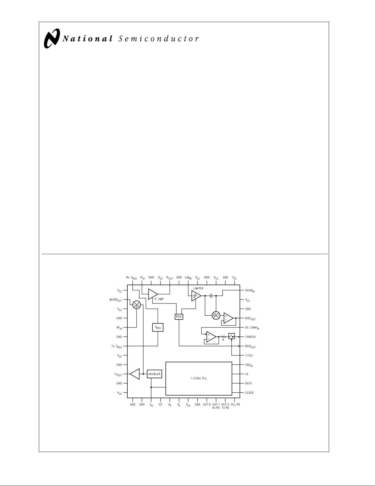
General Description
The LMX3162 Single Chip Radio Transceiverisamonolithic,
integrated radio transceiver optimized for use in ISM 2.45
GHz wireless systems. It is fabricated using National’s ABiC
V BiCMOS process (f
The LMX3162 contains phase locked loop (PLL), transmit
and receive functions. The 1.3 GHz PLL is shared between
transmit and receive sections. The transmitter includes a frequency doubler, and a high frequency buffer. The receiver
consists of a 2.5 GHz low noise mixer, an intermediate frequency (IF) amplifier, a high gain limiting amplifier, a frequency discriminator, a received signal strength indicator
(RSSI), and an analog DC compensation loop. The PLL,
doubler, and buffers can be used to implement open loop
modulation along with an external VCO and loop filter. The
circuit features on-chip voltage regulation to allow supply
voltages ranging from 3.0V to 5.5V. Two additional voltage
regulators provide a stable supply source to external discrete stages in the Tx and Rx chains.
The IF amplifier, high gain limiting amplifier, and discriminator are optimized for 110 MHz operation, with a total IF gain
of 85 dB. The single conversion receiver architecture provides a low cost, high performance solution for communications systems. The RSSI output may be used for channel
quality monitoring.
= 18 GHz).
T
Block Diagram
The Single Chip Radio Transceiver is available in a 48-pin
7mm X 7mm X 1.4mm PQFP surface mount plastic package.
Features
n Single chip solution for ISM 2.45 GHz RF transceiver
n System RF sensitivity to −93 dBm; RSSI sensitivity to
−100 dBm
n Two regulated voltage outputs for discrete amplifiers
n High gain (85 dB) intermediate frequency strip
n Allows unregulated 3.0V–5.5V supply voltage
n Power down mode for increased current savings
n System noise figure 6.5 dB (typ)
Applications
n ISM 2.45 GHz frequency band wireless systems
n Personal wireless communications (PCS/PCN)
n Wireless local area networks (WLANs)
n Other wireless communications systems
DS100929-1
MICROWIRE™is a trademark of National Semiconductor Corporation.
®
TRI-STATE
© 2000 National Semiconductor Corporation DS100929 www.national.com
is a registered trademark of National Semiconductor Corporation.
Page 2
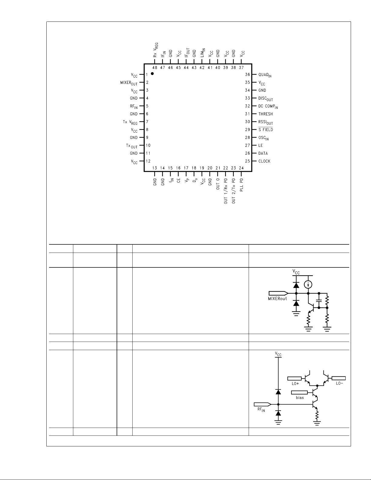
LMX3162 Connection Diagram
LMX3162
DS100929-2
Top View
Order Number LMX3162VBH or LMX3162VBHX
See NS Package Number VBH48A
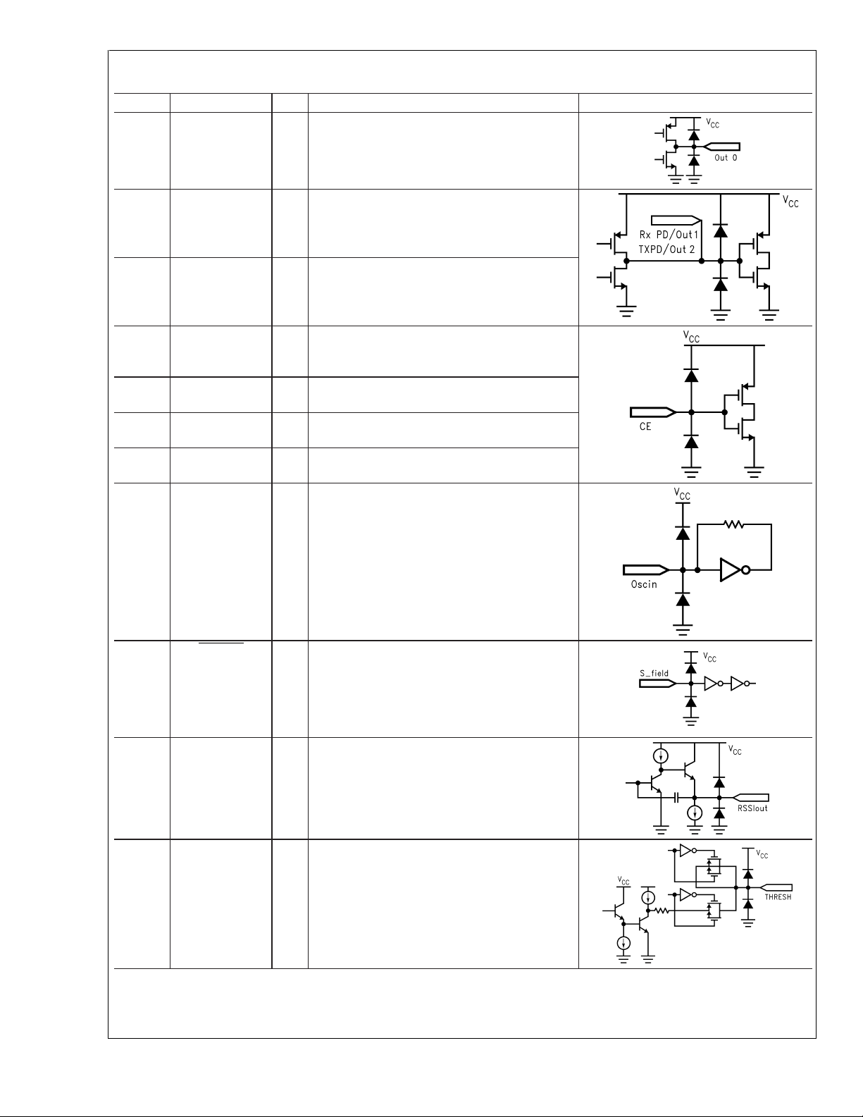
Pin Descriptions
Pin No. Pin Name I/O Description
1V
2 MIXER
CC
OUT
3VCC— Power supply for mixer section.
4 GND — Ground.
5RF
IN
— Power supply for CMOS section of PLL and
ESD bussing.
O IF output from the mixer.
I RF input to the mixer.
6 GND — Ground.
www.national.com 2
Page 3

Pin Descriptions (Continued)
Pin No. Pin Name I/O Description
7TxV
REG
8VCC— Power supply for analog sections of PLL and
9 GND — Ground.
10 Tx
OUT
11 GND — Ground.
12 V
CC
13 GND — Ground.
14 GND — Ground.
15 f
IN
— Regulated power supply for external PA gain
stage.
doubler.
O Frequency doubler output.
— Power supply for analog sections of PLL and
doubler.
I RF Input to PLL and frequency doubler.
LMX3162
16 CE I Chip Enable. Pulling LOW powers down entire
chip. Taking CE HIGH powers up the
appropriate functional blocks depending on the
state of bits F6, F7, F11, and F12 programmed
in F-latch. It is necessary to initialize the internal
registers once, after the power up reset. The
registers’ contents are kept even in power-down
condition.
17 V
18 D
P
o
— Power supply for charge pump.
O Charge pump output. For connection to a loop
filter for driving the input of an external VCO.
19 V
CC
— Power supply for CMOS section of PLL and
ESD bussing.
20 GND — Ground.
www.national.com3
Page 4
Pin Descriptions (Continued)
Pin No. Pin Name I/O Description
LMX3162
21 OUT 0 O Programmable CMOS output. Refer to Function
Register Programming Description section for
details.
22 Rx PD/OUT 1 I/O Receiver power down control input or
programmable CMOS output. Refer to Function
Register Programming Description section for
details.
23 Tx PD/OUT 2 I/O Transmitter power down control input or
programmable CMOS output. Refer to Function
Register Programming Description section for
details.
24 PLL PD I PLL power down control input. LOW for PLL
normal operations, and HIGH for PLL power
saving.
25 CLOCK I MICROWIRE™clock input. High impedance
CMOS input with Schmitt Trigger.
26 DATA I MICROWIRE data input. High impedance
CMOS input with Schmitt Trigger.
27 LE I MICROWIRE load enable input. High
impedance CMOS input with Schmitt Trigger.
28 OSC
IN
I Oscillator input. High impedance CMOS input
with feedback.
29 S FIELD I DC compensation circuit enable. While LOW,
the DC compensation circuit is enabled and the
threshold is updated through the DC
compensation loop. While HIGH, the switch is
opened, and the comparator threshold is held
by the external capacitor.
30 RSSI
31 THRESH O Threshold level to external comparator.
www.national.com 4
OUT
O Received signal strength indicator (RSSI)
output.
Page 5
Pin Descriptions (Continued)
Pin No. Pin Name I/O Description
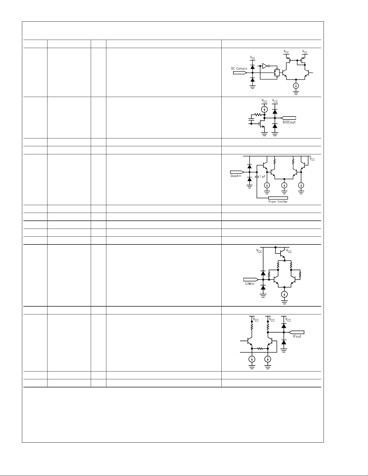
32 DC COMP
IN
I Input to DC compensation circuit.
LMX3162
33 DISC
OUT
O Demodulated output of discriminator.
34 GND — Ground.
35 V
CC
36 QUAD
37 V
CC
IN
— Power supply for the discriminator circuit.
I Quadrature input for tank circuit.
— Power supply for limiter output stage.
38 GND — Ground.
39 V
CC
— Power supply for limiter gain stages.
40 GND — Ground.
41 V
42 LIM
CC
IN
— Power supply for IF amplifier gain stages.
I IF input to the limiter.
43 GND — Ground.
44 IF
45 V
OUT
CC
O IF output from IF amplifier.
— Power supply for IF amplifier output.
46 GND — Ground.
www.national.com5
Page 6
Pin Descriptions (Continued)
Pin No. Pin Name I/O Description
LMX3162
47 IF
IN
I IF input to IF amplifier.
48 Rx V
REG
— Regulated power supply for external LNA
stages.
www.national.com 6
Page 7

LMX3162
Absolute Maximum Ratings (Notes 1, 2)
Power Supply Voltage (V
V
P
Voltage on Any Pin with
GND=0V(V
) −0.3V to VCC+0.3V
I
Storage Temperature Range (T
Lead Temp. (solder, 4 sec)(T
) −0.3V to +6.5V
CC
−0.3V to +6.5V
) −65˚C to +150˚C
S
) +260˚C
L
Recommended Operating
Conditions
Supply Voltage (VCC) 3.0V to 5.5V
)V
(V
P
Operating Temperature (T
Note 1: Absolute Maximum Ratings indicate limits beyond which damage to
the device may occur. Recommended Operating Conditions indicate conditions for which the device is intended to be functional, but do not guarantee
specific performance limits. For guaranteed specifications and test conditions, see the Electrical Characteristics section. The guaranteed specifications apply only for the test conditions listed.
Note 2: This device is a high performance RF integrated circuit with an ESD
<
KeV and is ESD sensitive. Handling and assembly of this device
rating
should only be done at ESD work stations.
) −10˚C to +70˚C
A
CC
to 5.5V
Electrical Characteristics
The following specifications are guaranteed for VCC= 3.6V and TA= 25˚C, unless otherwise specified.
Symbol Parameter Conditions Min Typ Max Unit
Current Consumption
I
CC, RX
I
CC, TX
I
CC, PLL
I
PD
MIXER f
f
RF
f
IF
Z
IN
Z
OUT
NF Noise Figure (Single Side Band) (Notes 5, 6) — 11.8 16 dB
G Conversion Gain (Note 5) 13 17 — dB
P
1dB
OIP3 Output 3rd Order Intercept Point (Note 5) — 7.5 — dBm
F
IN
F
IN
RF–IF RF to IF Isolation P
IF AMPLIFIER f
NF Noise Figure (Note 7) — 8 11 dB
A
V
Z
IN
Z
OUT
IF LIMITER f
Sens Limiter/Discriminator Sensitivity BER=10
IF
IN
DISCRIMINATOR f
V
OUT
V
OS
DISC
-Open-Loop Receive Mode PLL & TX chain powered down — 50 65 mA
-Open-Loop Transmit Mode PLL & RX chain powered down — 27 40 mA
-PLL only Mode RX & TX chain powered down — 6 9 mA
-Power Down Mode — — 70 µA
= 2.45 GHz, fIF= 110 MHz, fLO= 2340 MHz (fIN= 1170 MHz)
RF
RF Frequency Range (Note 3) 2.4 — 2.5 GHz
IF Frequency (Note 4) — 110 — MHz
Input Impedance, RF
IN
—
Output Impedance, Mixer Out —
12+j6
160−j65
— Ω
— Ω
Input 1dB Compression Point (Note 5) — −20 — dBm
-RF Fin to RF Isolation FIN=1170 MHz, RFOUT=1170 MHz — −30 — dB
F
=1170 MHz, RFOUT=2340 MHz — −20 — dB
IN
F
=1170 MHz, RFOUT=3510 MHz — −30 — dB
IN
-IF Fin to IF Isolation FIN=1170 MHz, IF
F
=1170 MHz, IF
IN
F
=1170 MHz, IF
IN
=0 to −85 dB — −30 — dB
IN
= 110 MHz
IN
=1170 MHz — −30 — dB
OUT
=2340 MHz — −30 — dB
OUT
=3510 MHz — −30 — dB
OUT
Gain (Note 7) 15 24 — dB
Input Impedance —
Output Impedance —
= 110 MHz
IN
−3
(Note 16) — −65 — dBm
IF Limiter Input Impedance —
= 110 MHz
IN
35–j180
210–j50
100–j300
— Ω
— Ω
— Ω
Disc Gain 1X Mode — 10 — mV/˚
(mV/˚ of Phase Shift from Tank Circuit) 3X Mode — 33 — mV/˚
Discriminator Output Peak to Peak 1X Mode (Note 8) 80 160 — mV
Voltage 3X Mode (Note 8) 400 580 — mV
Disc. Output DC Voltage Nominal (Note 10) 1.2 — 1.82 V
Disc. Output Impedance — 300 — Ω
OUT
www.national.com7
Page 8

Electrical Characteristics (Continued)
The following specifications are guaranteed for VCC= 3.6V and TA= 25˚C, unless otherwise specified.
LMX3162
Symbol Parameter Conditions Min Typ Max Unit
RSSI (Note 11) f
RSSI
Output Voltage PIN=−80 dBm@IFINinput pin 0.12 0.2 0.6 V
out
Slope P
RSSI Dynamic Range P
DC COMPENSATION CIRCUIT
V
OS
V
I/O
R
SH
Input Offset Voltage −6 — +6 mV
Input/Output Voltage Swing Centered at 1.5V — 1.0 — V
Sample and Hold Resistor 2000 3000 3600 Ω
FREQUENCY SYNTHESIZER
f
IN
P
IN
f
OSC
V
OSC
I
Do-source
I
Do-sink
I
Do-source
I
Do-sink
I
Do-Tri
Input Frequency Range (Note 9) 1100 — 1300 MHz
Input Signal Level ZIN=200Ω (Note 15) — −11.5 — dBm
Oscillator Frequency Range (Note 12) 5 — 20 MHz
Oscillator Sensitivity (Note 12) 0.5 1.0 — V
Charge Pump Output Current Vdo=VP/2, I
FREQUENCY DOUBLER(Note 17) f
f
P
OUT
OUT
Output Frequency Range (Note 13) 2250 — 2500 MHz
Output Signal Level PIN= −11.5 dBm, f
Fundamental Output Power P
Harmonic Output Power P
VOLTAGE REGULATOR
V
O
Output Voltage I
DIGITAL INPUT/OUTPUT PINS
V
IH
V
IL
I
IH
V
OH
V
OL
Note 3: The mixer section is tested at 2.45 GHz.
Note 4: The IF section of this device is designed for optimum performance at 110 MHz.
Note 5: The matching network used on RF
sists of a series 150 nH inductance and a shunt 15 pF capacitance into the pin.
Note 6: Noise figure measurements are made with matching networks on RF
Note 7: The matching network used on pin IF
ing network used on pin IF
Note 8: The discriminator is with the DC level centered at 1.5V. The unloaded Q of the tank is 40.
Note 9: The frequency synthesizer section is tested at 1.225 GHz.
Note 10: Nominal refers to zero DC offsets programmed for the discriminator.
Note 11: It depends on loss of the inter-stage filter. These specifications are for an inter-stage loss of 8 dB.
Note 12: The frequency synthesizer section is guaranteed by design to operate for OSC
0.5 V
Note 13: The doubler section is tested at 2.45 GHz.
Note 14: See Function Register Programming Description for Icp
High Level Input Voltage 2.4 — — V
Low Level Input Voltage — — 0.8 V
Input Current GND<V
High Level Output Voltage IOH=−0.5 mA 2.4 — — V
Low Level Output Voltage IOL=0.5 mA — — 0.4 V
for this measurement consists of a series 3.3 pF capacitance into the pin. The matching circuit used on MIXER
IN
for this measurement conists of a series 330 nH inductance and a shunt 2.7 pF capacitance into the pin. The match-
consists of a series 120 nH inductance and a shunt 12 pF into the pin..
OUT
.
PP
IN
= 110 MHz
IN
P
=−20 dBm@IFINinput pin 0.9 1.2 — V
IN
= −85 to −25 dBm@IFINinput pin 10 18 25 mV/dB
IN
min= −90 dBm@IFINinput pin — 60 — dB
IN
cpo
= LOW
— −1.5 — mA
(Note 14)
Vdo=VP/2, I
cpo
= LOW
— 1.5 — mA
(Note 14)
Vdo=VP/2, I
cpo
= HIGH
— −6.0 — mA
(Note 14)
Vdo=VP/2, I
CPO
= HIGH
— 6.0 — mA
(Note 14)
0.5 ≤ Vdo≤ Vp− 0.5
= 25˚C
T
A
= 1225 MHz, f
IN
= −11.5 dBm, f
IN
= −11.5 dBm, f
IN
= 5 mA 2.55 2.75 2.90 V
LOAD
<
IN
and MIXER
IN
description.
o
= 2.45 GHz
OUT
= 2.45 GHz −12 −7.5 — dBm
OUT
= 1225 MHz — −17 −10 dBm
OUT
= 3.675 GHz — −30 −15.5 dBm
OUT
V
CC
. See (Note 5).
OUT
input frequency within 5–20 MHz range and minimum amplitude of
IN
−1.0 — 1.0 nA
−10 — 10 µA
OUT
PP
pp
con-
www.national.com 8
Page 9

Electrical Characteristics (Continued)
Note 15: Tested in a 50Ω environment.
Note 16: The matching network used on pin LIM
Note 17: The optimum load as seen by the TX OUT pin should be between 50 and 100 ohms.
for this measurement consists of a series 330 nH inductance and a shunt 1.8 pF into the pin.
IN
Typical Performance Characteristics
LMX3162
Mixer P
F
Power with RFIN=
IN
−51 dBm,
vs
OUT
@
2450 MHz, 25˚C
RSSI Output vs
Input Power to IF
IN
with VCCas Parameter
DS100929-16
Mixer P
F
Power with RFIN=
IN
−51 dBm,
vs
OUT
@
2450 MHz, VCC=3.6V
IDOTRI-STATE™vs
D
Voltage, VCC=5.5V
O
DS100929-17
DS100929-18
DS100929-19
www.national.com9
Page 10

Typical Performance Characteristics (Continued)
LMX3162
Charge Pump Current vs
D
Voltage VCC=3.6V, 25˚C
O
Charge Pump Current vs
D
Voltage, VCC=3.0V, 25˚C
O
DS100929-20
Mixer OIP3 vs FINPower
DS100929-43
Mixer Output Power vs Mixer Input Power
DS100929-21
Mixer Gain vs FINPower
DS100929-44
Mixer Gain vs RFINFrequency
DS100929-45
www.national.com 10
DS100929-46
Page 11

Typical Performance Characteristics (Continued)
LMX3162
SSB Mixer Noise Figure vs RF
TX Power Out vs FINPower
Frequency
IN
DS100929-47
SSB Mixer Noise Figure vs FINPower
DS100929-48
TX Power Out vs FINFrequency
DS100929-49
DS100929-50
AC Timing Characteristics
Serial Data Input Timing
TEST CONDITIONS: The Serial Data Input Timing is tested using a symmetrical waveform around VCC/2. The test waveform has
an skew rate of 0.6V/ns.
DS100929-3
Notes: Parenthesis data indicates programmable reference divider data.
Data shifted into register on clock rising edge.
Data is shifted in MSB first.
www.national.com11
Page 12

Serial Data Input Timing (Continued)
Symbol Parameter Conditions Min Typ Max Unit
LMX3162
MICROWIRE
t
CS
t
CH
t
CWH
t
CWL
t
ES
t
EW
™
Interface
Data to Clock Set Up Time Refer to Test Condition. 50 — — ns
Data to Clock Hold Time Refer to Test Condition. 10 — — ns
Clock Pulse Width High Refer to Test Condition. 50 — — ns
Clock Pulse Width Low Refer to Test Condition. 50 — — ns
Clock to Load Enable Set Up Time Refer to Test Condition. 50 — — ns
Load Enable Pulse Width Refer to Test Condition. 50 — — ns
PLL Functional Description
The simplified block diagram below shows the building blocks of frequency synthesizer and all internal registers, which are 20-bit
data register, 18-bit F-latch, 13-bit N-counter, and 5-bit R-counter.
DS100929-4
The DATAstream is clocked into the data register on the rising edge of CLOCK signal, MSB first. The last two bits are the control
bits to indicate which register to be written. Upon the rising edge of the LE (Load Enable) signal, the rest of data bits is transferred
to the addressed register accordingly. The decoding scheme of the two control bits is as follows:
Control Bits Register
C2 C1
0 0 N-Counter
1 0 R-Counter
X 1 F-Latch
Note: X = Don’t Care Condition
Programmable Feedback Divider (N-Counter)
The N-counter consists of the 6-bit swallow counter (A-counter) and the 7-bit programmable counter (B-counter). When the control bits are “00”, data is transferred from the 20-bit shift register into two latches. One latch sets the A-counter while the other sets
the B-counter. The serial data format is shown below.
MSB REGISTER’S BIT MAPPING LSB
19 181716 15 14131211 10 9 8 7 6 543210
RESERVED N-COUNTER’s Divide Ratio C2 C1
X XXXXN13N12N11N10N9N8N7N6N5N4N3N2N100
Note: X = Don’t Care Condition
Swallow Counter Divide Ratio (A-Counter)
Divide Ratio, A N6 N5 N4 N3 N2 N1
0 000000
1 000001
* ******
63 111111
www.national.com 12
Page 13

Swallow Counter Divide Ratio (A-Counter) (Continued)
Note: Divide ratio must be from 0 to 63, and B must be ≥ A.
Programmable Counter Divide Ratio (B-Counter)
Divide Ratio, B N13 N12 N11 N10 N9 N8 N7
3 0000011
4 0000100
* *******
127 1111111
Note: Divide ratio must be from 3 to 127, and B must be ≥ A.
Programmable Reference Divider (R-Counter)
If the control bits are “10”, data is transferred from the 20-bit shift register into a latch, which sets the 5-bit R-counter.The serial
data format is shown below.
MSB REGISTER’S BIT MAPPING LSB
19 1817161514131211109876543210
RESERVED R-COUNTER’s Divide
Ratio
X XXXXXXXXXXXXR5R4R3R2R110
Note: X = Don’t Care Condition
C2 C1
LMX3162
Reference Counter Divide Ratio (R-Counter)
Divide Ratio, R R5 R4 R3 R2 R1
3 00011
4 00100
* *****
31 11111
Note: Divide ratio must be from 3 to 31.
Pulse Swallow Function
f
:
Output frequency of external voltage controlled oscillator (VCO)
vco
B:
Preset divide ratio of binary 7-bit programmable counter (3 to 127)
A:
Preset divide ratio of binary 6-bit swallow counter (0 ≤ A ≤ P, A ≤ B)
f
:
Output frequency of the external reference frequency oscillator
OSC
R:
Preset divide ratio of binary 5-bit programmable reference counter (3 to 31)
P:
Preset modulus of dual modulus prescaler (32 or 64)
Receiver Functional Description
The simplified block diagram below shows the mixer, IF amplifier,limiter, and discriminator. In addition, the DC compensation circuit, doubler, and voltage regulator for an external LNA stage are shown.
www.national.com13
Page 14

Receiver Functional Description (Continued)
LMX3162
DS100929-5
Note 18: The receiver can be powered down, either by hardware through the Rx PD pin, or by software through the programming of F6 bit in the F-Latch.The power
down control method is determined by the settings of F11 and F12 in F-Latch. (Refer to Function Register Programming Description section for details.)
Note 19: The internal capacitor of the discriminator has a value of 1 pF, and has been optimized for operation at 110 MHz.
Transmitter Functional Description
The simplified block diagram below shows the doubler and voltage regulator for an external transmit gain stage.
DS100929-6
Note: The transmitter can be powered down, either by hardware through the Tx PD pin, or by software through the programming of F7 bith in F-Latch. The
power down control method is determined by the settings of F11 and F12 in F-Latch. (Refer to Function Register Programming Description section for details.)
Function Register Programming Description (F-Latch)
If the control bits are “1X”, data is transferred from the 20-bit shift register into the 18-bit F-latch. Serial data format is shown
below.
MSB REGISTER’S BIT MAPPING LSB
19 1817161514131211109876543210
MODE CONTROL WORD C2 C1
F18 F17 F16 F15 F14 F13 F12 F11 F10 F9 F8 F7 F6 F5 F4 F3 F2 F1 X 1
Note: X = Don’t Care Condition
Various modes of operation can be programmed with the function register bits F1–F18, including the phase detector polarity,
charge pump TRI-STATE and CMOS outputs. In addition, software or hardwire power down modes can be specified with bits F11
and F12.
www.national.com 14
Page 15

Function Register Programming Description (F-Latch) (Continued)
LMX3162
Mode
Control
Bit
F1 Prescaler modules select. 32/33 64/65
F2 Phase detector polarity. It is used to reverse the polarity of
the phase detector according to the VCO characteristics.
F3 Charge pump current gain select. LOW Charge Pump
F4 TRI-STATE charge pump output. Normal Operation Force to TRI-STATE
F5 Reserved. Setting to “0” always. — —
F6 Receive chain power down control. Software power down
can only be activated when both F11 and F12 are set to “0”.
F7 Transmit chain power down control. Software power down
can only be activated when both F11 and F12 are set to “0”.
F8 Out 0 CMOS output. OUT 0 = LOW OUT 0 = HIGH
F9 Out 1 CMOS output. Functions only in software power down
mode, when both F11 and F12 are set to “0”.
F10 Out 2 CMOS output. Functions only in software power down
mode, when both F11 and F12 are set to “0”.
F11
F12
F13 Demodulator gain select 1X Gain Mode 3X Gain Mode
F14 Demodulator DC level shift +/− level shifting polarity Set Negative Polarity Set Positive Polarity
F15 Demodulator DC level shift of 1.000V No Shift Shift the DC Level
F16 Demodulator DC level shift of 0.500V No Shift Shift the DC Level
F17 Demodulator DC level shift of 0.250V No Shift Shift the DC Level
F18 Demodulator DC level shift of 0.125V No Shift Shift the DC Level
Power down mode select.
Set both F11 and F12 to “0” for software power down mode.
Set both F11 and F12 to “1” for hardwire power down mode.
Other combinations are reserved for test mode.
Mode Control Description
Setting to
“0” to Select
Negative VCO
Characteristics
Current (1X I
Power Up RX Chain Power Down RX Chain
Power Up TX Chain Power Down TX Chain
OUT 1 = LOW OUT 1 = HIGH
OUT 2 = LOW OUT 2 = HIGH
Software
Power Down
cpo
).
Setting to
“1” to Select
Positive VCO
Characteristics
HIGH Charge Pump
Current (4X I
Hardware
Power Down
by 1.000V
by 0.500V
by 0.250V
by 0.125V
cpo
).
Power Down Mode/Control Table
Software Power Down Mode (F11=F12=0) Hardwire Power Down Mode (F11=F12=1)
Pin/Bit Setting to “0”
means
F6 Receiver ON Receiver OFF Rx PD Receiver OFF Receiver ON
F7 Transmitter ON Transmitter OFF Tx PD Transmitter OFF Transmitter ON
PLL PD PLL ON PLL OFF PLL PD PLL ON PLL OFF
CE LMX3162 OFF LMX3162 ON CE LMX3162 OFF LMX3162 ON
Setting to “1”
means
Pin/Bit Setting to “0”
means
Setting to “1”
means
www.national.com15
Page 16

Typical Application
LMX3162
DS100929-7
www.national.com 16
Page 17

Loop Filter Design Consideration
FIGURE 1. Conventional PLL Architecture
LMX3162
DS100929-8
Loop Gain Equations
A linear control system model of the phase feedback for a
PLL in the locked state is shown in
gain is the product of the phase comparator gain (K
VCO gain (K
/s), and the loop filter gain Z(s) divided by the
vco
gain of the feedback counter modulus (N). The passive loop
filter configuration used is displayed in
complex impedance of the filter is given in
FIGURE 2. PLL Linear Model
FIGURE 3. Passive Loop Filter
Figure 2
Figure 3
DS100929-10
. The open loop
), the
φ
, while the
Equation (2)
.
DS100929-9
PASSIVE LOOP FILTER
Open loop gain = H(s) G(s) =
θi/θe=K
Z(s)K
φ
/Ns (1)
VCO
(2)
The time constants which determine the pole and zero frequencies of the filter transfer function can be defined as
(3)
and
T2=R2•C2
(4)
The 3rd order PLL Open Loop Gain can be calculated in
terms of frequency, ω, the filter time constants T1 and T2,
and the design constants K
φ,Kvco
, and N.
(5)
From
Equations (3), (4)
we can see that the phase term will
be dependent on the single pole and zero such that the
phase margin is determined in
φ (ω) = tan
−1
(ω
T
2) − tan−1(ω
•
Equation (6)
•
.
T
1) + 180˚ (6)
www.national.com17
Page 18

Physical Dimensions inches (millimeters) unless otherwise noted
LMX3162 Single Chip Radio Transceiver
48-Lead (7mm x 7mm) Molded Plastic Quad Flat Package, JEDEC
For Tape and Reel (2500 Units per Reel)
Order Number LMX3162VBH or LMX3162VBHX
NS Package Number VBH48A
LIFE SUPPORT POLICY
NATIONAL’S PRODUCTS ARE NOT AUTHORIZED FOR USE AS CRITICAL COMPONENTS IN LIFE SUPPORT
DEVICES OR SYSTEMS WITHOUT THE EXPRESS WRITTEN APPROVAL OF THE PRESIDENT AND GENERAL
COUNSEL OF NATIONAL SEMICONDUCTOR CORPORATION. As used herein:
1. Life support devices or systems are devices or
systems which, (a) are intended for surgical implant
into the body, or (b) support or sustain life, and
whose failure to perform when properly used in
accordance with instructions for use provided in the
2. A critical component is any component of a life
support device or system whose failure to perform
can be reasonably expected to cause the failure of
the life support device or system, or to affect its
safety or effectiveness.
labeling, can be reasonably expected to result in a
significant injury to the user.
National Semiconductor
Corporation
Americas
Tel: 1-800-272-9959
Fax: 1-800-737-7018
Email: support@nsc.com
www.national.com
National Semiconductor
Europe
Fax: +49 (0) 180-530 85 86
Email: europe.support@nsc.com
Deutsch Tel: +49 (0) 69 9508 6208
English Tel: +44 (0) 870 24 0 2171
Français Tel: +33 (0) 1 41 91 8790
National Semiconductor
Asia Pacific Customer
Response Group
Tel: 65-2544466
Fax: 65-2504466
Email: ap.support@nsc.com
National Semiconductor
Japan Ltd.
Tel: 81-3-5639-7560
Fax: 81-3-5639-7507
National does not assume any responsibility for use of any circuitry described, no circuit patent licenses are implied and National reserves the right at any time without notice to change said circuitry and specifications.
 Loading...