

Page 1
User's Guide
SNAU217A–August 2017–Revised November 2017
LMX2572EVM Evaluation Instructions
The LMX2572EVM is design to evaluate the performance of LMX2572. This board consists of a LMX2572
device.
The LMX2572 is a low-power, high-performance wideband synthesizer that can generate any frequency
from 12.5 MHz to 6.4 GHz without using an internal VCO doubler. The PLL delivers excellent performance
while consuming just 75 mA from a single 3.3-V supply.
1 LMX2572EVM Evaluation Module......................................................................................... 3
2 Setup .......................................................................................................................... 3
3 Typical Measurement ....................................................................................................... 5
4 Schematic ................................................................................................................... 13
5 PCB Layout and Layer Stack-up......................................................................................... 15
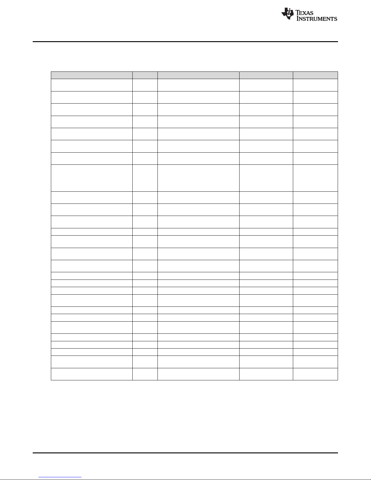
6 Bill of Materials ............................................................................................................. 18
7 Troubleshooting Guide .................................................................................................... 19
Appendix A Using Different Reference Clock ................................................................................ 20
Appendix B Reference PRO.................................................................................................... 21
1 EVM Connection Diagram.................................................................................................. 3
2 Select Device in TICS Pro.................................................................................................. 4
3 Default Mode ................................................................................................................. 5
4 MUXout_SW Switch......................................................................................................... 5
5 Loop Filter .................................................................................................................... 6
6 Default Output................................................................................................................ 6
7 Phase Adjustment Setting .................................................................................................. 7
SNAU217A–August 2017–Revised November 2017
Submit Documentation Feedback
Contents
List of Figures
Copyright © 2017, Texas Instruments Incorporated
LMX2572EVM Evaluation Instructions
1
Page 2

www.ti.com
8 Phase Adjustment ........................................................................................................... 7
9 Calibration-Free Automatic Ramp Setting................................................................................ 8
10 Calibration-Free Automatic Ramp ......................................................................................... 8
11 Automatic Ramp Setting.................................................................................................... 9
12 Automatic Ramp ............................................................................................................. 9
13 SYSREF Pulsed Mode Setting........................................................................................... 10
14 SYSREF Pulsed Mode .................................................................................................... 10
15 FSK SPI FAST Mode Setting............................................................................................. 11
16 FSK SPI FAST Mode...................................................................................................... 11
17 Readback Setting .......................................................................................................... 12
18 Register Readback......................................................................................................... 12
19 LMX2572EVM Schematic (Page 1)...................................................................................... 13
20 LMX2572EVM Schematic (Page 2)...................................................................................... 14
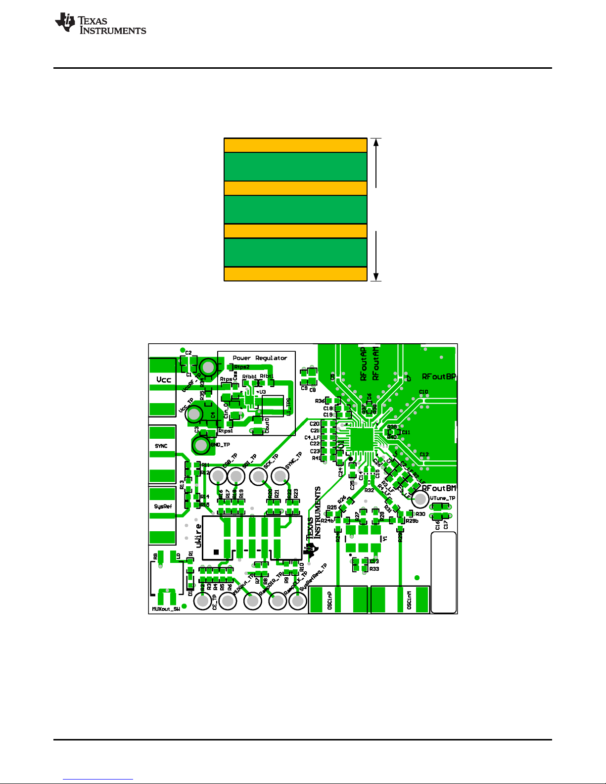
21 PCB Layer Stack-Up....................................................................................................... 15
22 Top Layer ................................................................................................................... 15
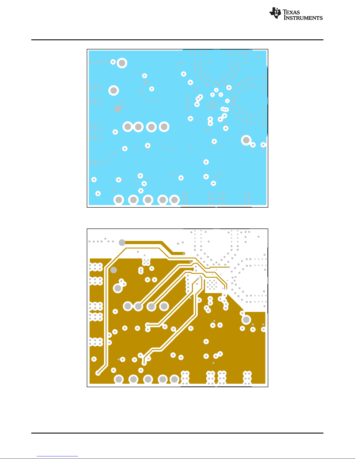
23 GND Layer .................................................................................................................. 16
24 Power Layer ................................................................................................................ 16
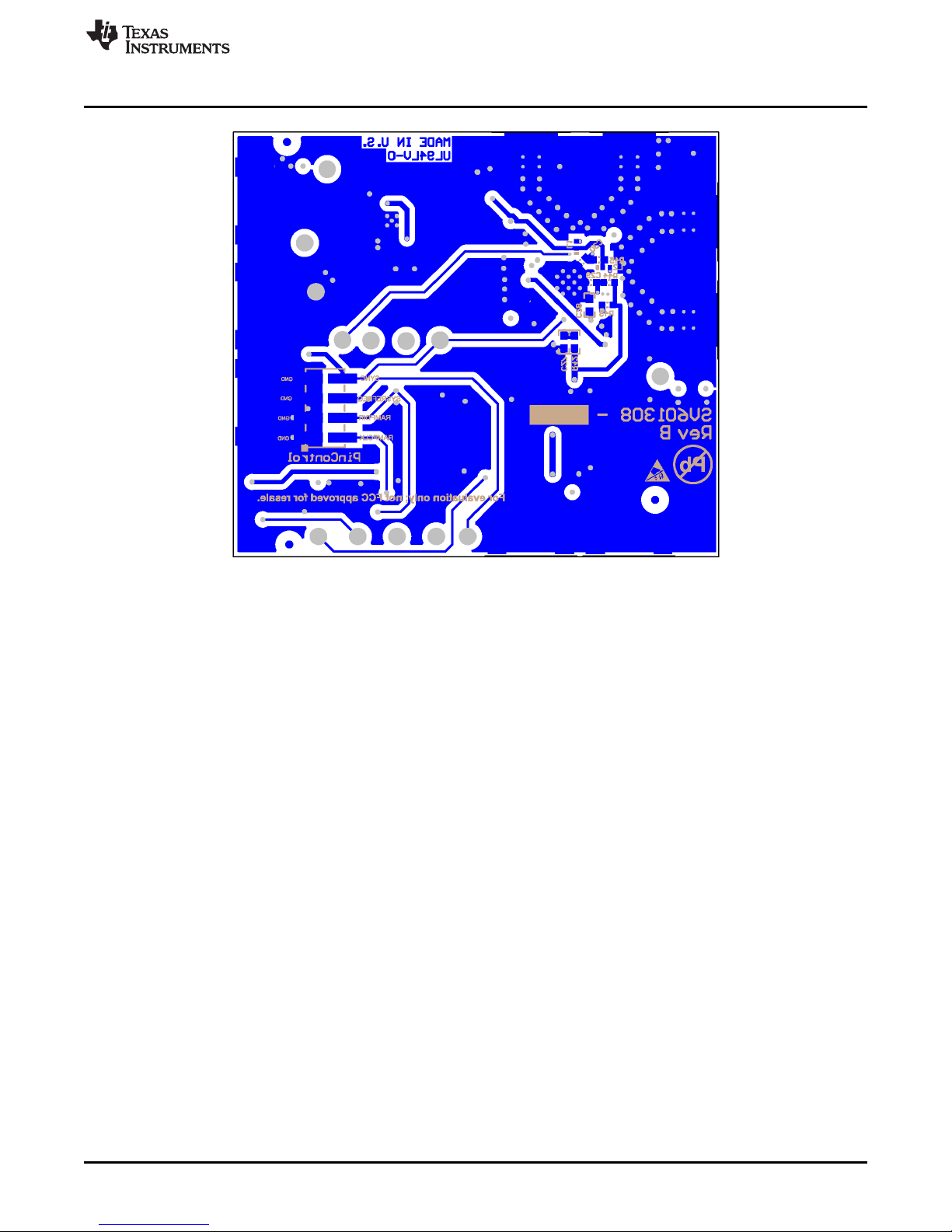
25 Bottom Layer................................................................................................................ 17
26 Troubleshooting Guide .................................................................................................... 19
27 Output Termination Schematic ........................................................................................... 22
28 Default Output Phase Nosie.............................................................................................. 23
29 Default Output Waveform ................................................................................................. 23
30 Firmware Requirement .................................................................................................... 23
31 Firmware Loader ........................................................................................................... 24
32 BSL Button .................................................................................................................. 24
33 Update Firmware........................................................................................................... 25
34 Firmware Update Completed ............................................................................................. 25
35 USB Communications ..................................................................................................... 26
1 Loop Filter Configuration.................................................................................................... 5
2 Phase Adjustment Setting .................................................................................................. 7
3 Calibration-free Automatic Ramp Example............................................................................... 8
4 Automatic Ramp Example.................................................................................................. 9
5 FSK SPI FAST Mode Example........................................................................................... 11
6 Bill of Materials ............................................................................................................. 18
7 Reference Clock Input Configuration.................................................................................... 20
8 Reference PRO Output Frequency Selection .......................................................................... 21
9 Reference PRO Output Format Selection .............................................................................. 22
10 Output Termination Configuration........................................................................................ 22
Trademarks
All trademarks are the property of their respective owners.
2
LMX2572EVM Evaluation Instructions
List of Tables
SNAU217A–August 2017–Revised November 2017
Copyright © 2017, Texas Instruments Incorporated
Submit Documentation Feedback
Page 3

50
50
www.ti.com
1 LMX2572EVM Evaluation Module
1.1 Evaluation Module Contents
In the box, there are:
• One LMX2572EVM board (SV601308-003).
• One Reference PRO board (SV601349).
• Two SMA Male-to-Male adaptors (132168).
• One USB cable.
• One 10-pin ribbon cable.
1.2 Evaluation Setup Requirement
The evaluation will require the following hardware and software:
• A DC power supply
• A spectrum analyzer or a signal analyzer
• A PC running Windows 7 or more recent version
• An oscilloscope (optional)
• A high quality signal generator (optional)
• Texas Instruments Clocks and Synthesizers TICS Pro software
• Texas Instruments PLLatinum Simulator Tool (optional)
LMX2572EVM Evaluation Module
1.3 Resources
Related evaluation and development resources are as follows:
• LMX2572 data sheet
• TICS Pro software
• PLLatinum Simulator Tool (PLL Sim)
2 Setup
2.1 Connection Diagram
SNAU217A–August 2017–Revised November 2017
Submit Documentation Feedback
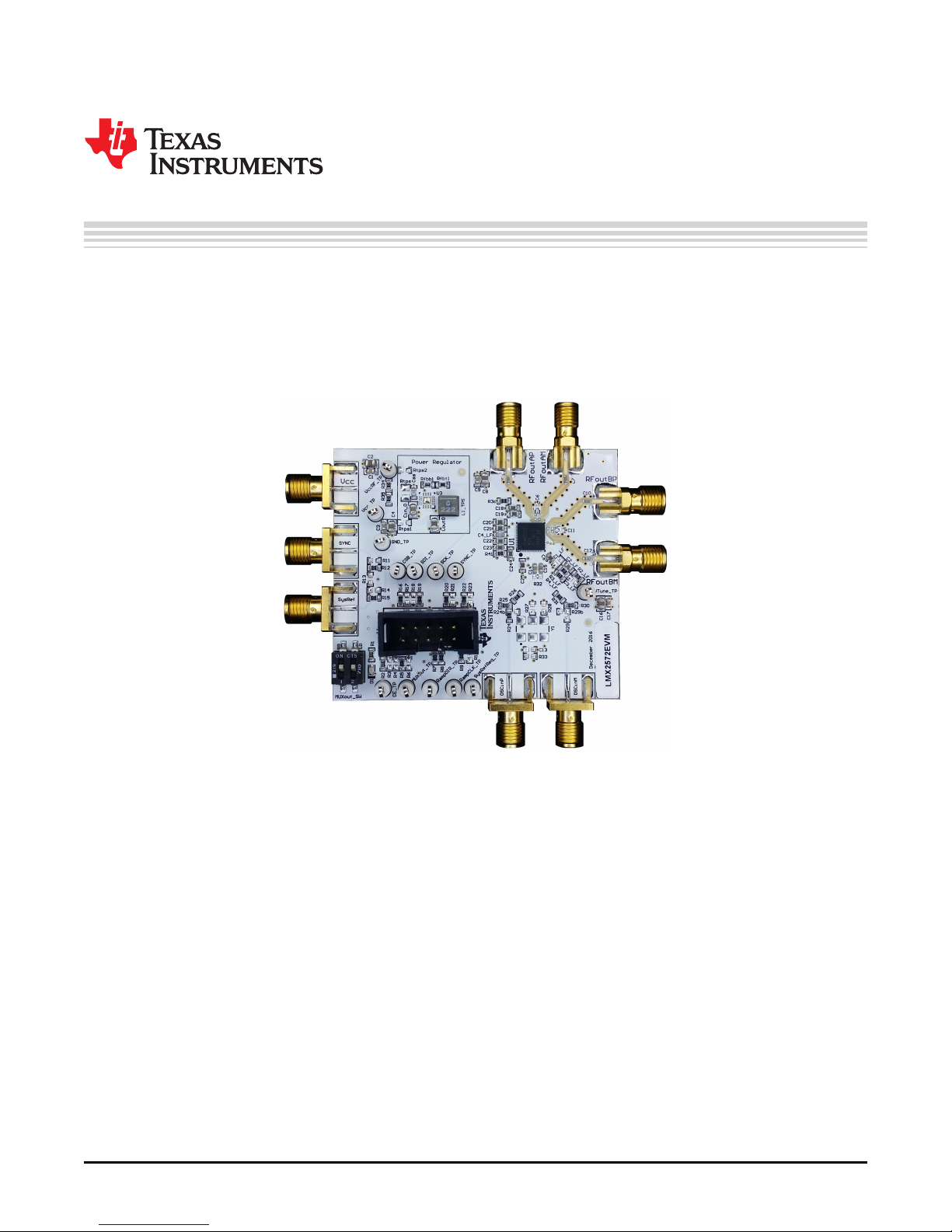
Figure 1. EVM Connection Diagram
Copyright © 2017, Texas Instruments Incorporated
LMX2572EVM Evaluation Instructions
3
Page 4
Setup
2.2 Power Supply
Apply 3.3 V to VCCSMA connector. Acceptable supply voltage range is 3 V to 3.6 V. The maximum current
consumption in the most extreme configuration must not exceed 150 mA.
By default, the onboard DC-DC converter is not used.
2.3 Reference Clock
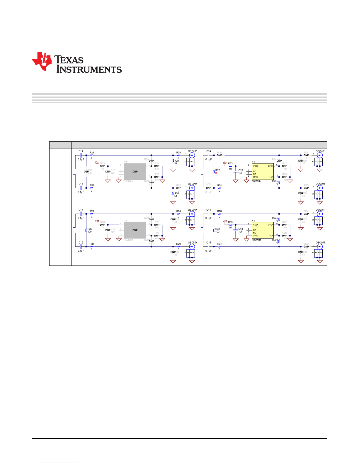
Connect OSCinP SMA connector with one of the outputs from Reference PRO using the SMA Male-tomale adopter. OSCinM SMA connector is not connected to LMX2572 so it could be left open.
The EVM is configured for single-ended input with OSCin pin connected to OSCinP SMA connector and
OSCinM pin 50-Ω terminated onboard. If required, the EVM can be modified to operate with different clock
source in different configuration, see Appendix A for details.
Terminate the unused output of the Reference PRO board with a 50-Ω resistor or SMA load. By default,
the output clock from Reference PRO is a 100-MHz LVPECL clock. Appendix B has the details of
Reference PRO.
2.4 RF Output
Connect either RFoutAP or RFoutAM SMA connector to a signal analyzer. The unused connector must be
terminated with a 50-Ω resistor or SMA load. Output frequency is 3 GHz and the amplitude is about +2.5
dBm.
By default, the evaluation software, TICS Pro, has RFoutB power down. These SMA connectors could be
left open.
www.ti.com
2.5 Programming
Connect ribbon cable from Reference PRO to LMX2572EVM.
Connect USB cable from a PC to USB port in Reference PRO. This provides power supply to Reference
PRO board and communication with TICS Pro. A firmware update may be required, see Appendix B for
details.
2.6 Evaluation Software
Download and install TICS Pro to a PC.
Run the software and follow the following steps to get started.
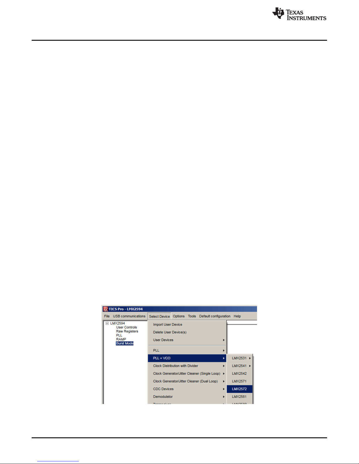
1. Go to "Select Device" → "PLL + VCO" → LMX2572.
2. Go to "Default Configuration" → "Default Mode xxxx-xx-xx".
4
LMX2572EVM Evaluation Instructions
Figure 2. Select Device in TICS Pro
SNAU217A–August 2017–Revised November 2017
Copyright © 2017, Texas Instruments Incorporated
Submit Documentation Feedback
Page 5
www.ti.com
2.7 EVM Strap Options
2.7.1 MUXout_SW
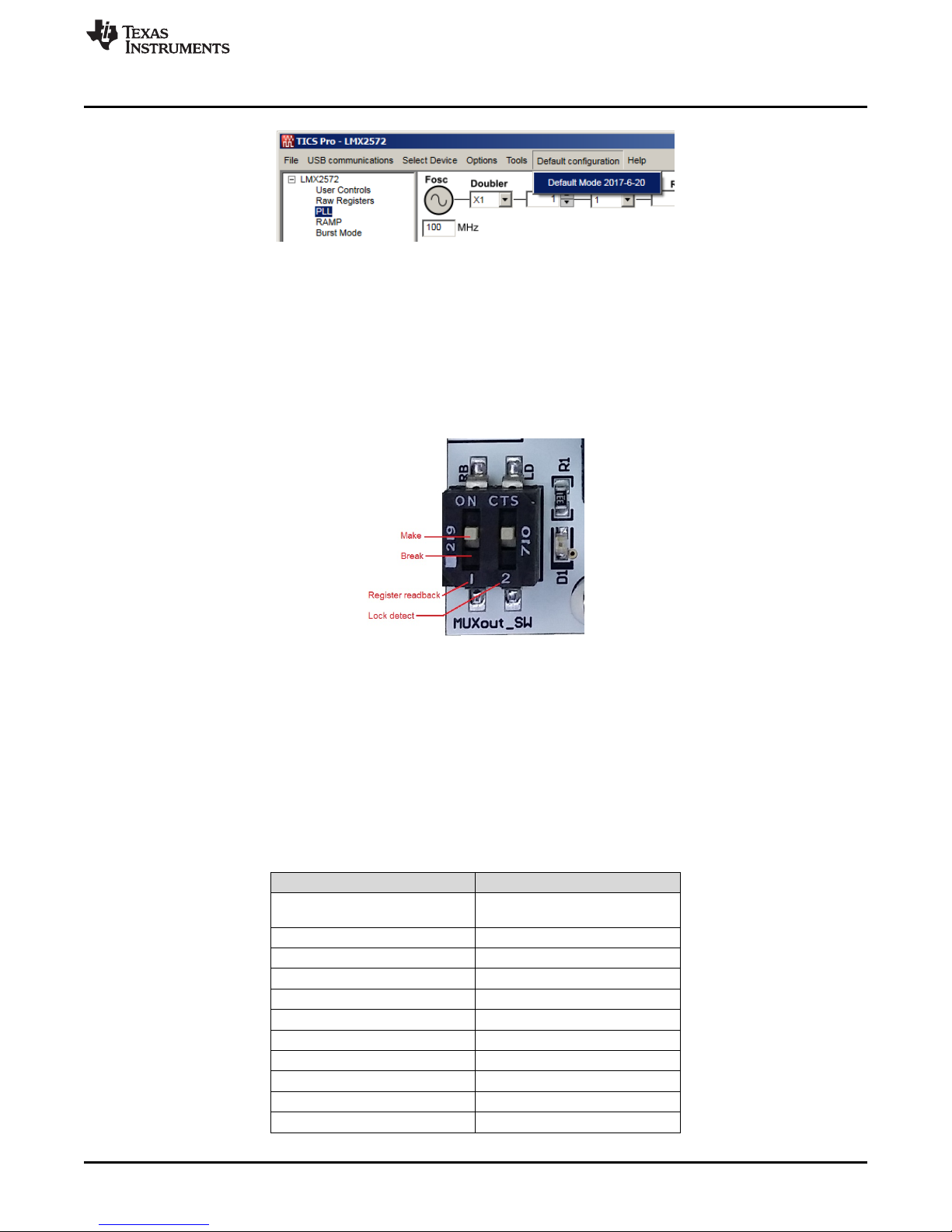
There are two switches in MUXout_SW. Switch 1 is used for register readback. Switch 2 is used to
provide a visual PLL lock status through the LED D1. By default, both switches are in the Make position.
To read back register in TICS Pro, set Switch 2 to the Break position.
Setup
Figure 3. Default Mode
3 Typical Measurement
3.1 Default Configuration
3.1.1 Loop Filter
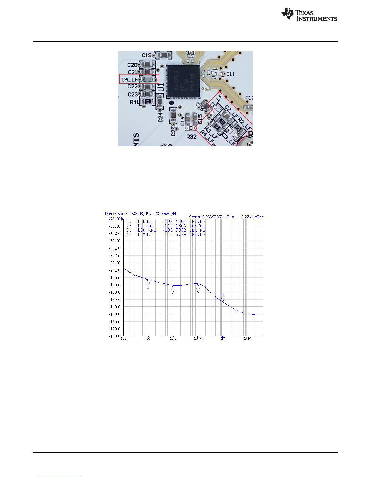
The parameters for the loop filter are:
Figure 4. MUXout_SW Switch
Table 1. Loop Filter Configuration
PARAMETER VALUE
VCO frequency
VCO gain 66 MHz/V
Effective charge pump gain 2500 µA
Phase detector frequency 100 MHz
Loop bandwidth 115 kHz
Phase margin 48 degrees
C1_LF, C3_LF Open
C2_LF 15 nF
C4_LF 2.2 nF
R2_LF 330 Ω
R3_LF, R4_LF 0 Ω
Designed for 6 GHz, but works
over the whole frequency range
SNAU217A–August 2017–Revised November 2017
Submit Documentation Feedback
Copyright © 2017, Texas Instruments Incorporated
LMX2572EVM Evaluation Instructions
5
Page 6
Typical Measurement
3.1.2 Typical Output
1. Follow Section 2 to setup the evaluation.
2. Click "Write All Registers" to write all the registers to LMX2572.
Default output is 3 GHz.
www.ti.com
Figure 5. Loop Filter
3.2 Additional Tests
3.2.1 Phase Adjustment
The phase of the RF output signal can be adjusted as follows:
Phase shift in degree = 360° × (MASH_SEED / PLL_DEN) × (P / CHDIV), where P = 2 when
VCO_PHASE_SYNC_EN = 1, else P = 1.
Here is an example.
6
LMX2572EVM Evaluation Instructions
Figure 6. Default Output
SNAU217A–August 2017–Revised November 2017
Copyright © 2017, Texas Instruments Incorporated
Submit Documentation Feedback
Page 7

www.ti.com
Phase shift = 360° × (800 / 1000) × (1 / 32) = 9°. We can write 800 to MASH_SEED 40 times to get 360°
phase shift.
Typical Measurement
Table 2. Phase Adjustment Setting
PARAMETER EXAMPLE VALUE
MASH_SEED 800
PLL_DEN 1000
CHDIV 32
VCO_PHASE_SYNC_EN 0
Figure 7. Phase Adjustment Setting
3.2.2 Calibration-free Automatic Ramping
LMX2572 supports linear frequency ramp without the need of VCO calibration in the middle of the ramp.
The output waveform is a continuous frequency sweep between the start and the end frequencies.
However, the frequency ramp range is limited. When using ramp, the followings need to be set
accordingly:
• OUT_FORCE = 1
• LD_DLY = 0
• PLL_DEN = 232– 1
SNAU217A–August 2017–Revised November 2017
Submit Documentation Feedback
Figure 8. Phase Adjustment
Copyright © 2017, Texas Instruments Incorporated
LMX2572EVM Evaluation Instructions
7
Page 8

Typical Measurement
This is a triangular ramp example. Ramp up is defined by RAMP0 while ramp down is defined by RAMP1.
RAMP_THRESH, RAMP_DLY_CNT, and RAMP_SCALE_COUNT are "don't care" because we are not
going to trigger any VCO calibration. RAMP_MANUAL = 0 means Automatic Ramping mode.
Set RAMP_EN = 1 to start ramping. Set RAMP_EN = 0 to turn off ramping.
www.ti.com
Table 3. Calibration-free Automatic Ramp Example
PARAMETER EXAMPLE VALUE
Ramping start frequency 4795 MHz
Ramping stop frequency 4805 MHz
Phase detector frequency 50 MHz
Ramp up / down time 200 µs
RAMP_LIMIT_HIGH 4995 MHz
RAMP_LIMIT_LOW 4595 MHz
Figure 9. Calibration-Free Automatic Ramp Setting
Figure 10. Calibration-Free Automatic Ramp
8
LMX2572EVM Evaluation Instructions
SNAU217A–August 2017–Revised November 2017
Copyright © 2017, Texas Instruments Incorporated
Submit Documentation Feedback
Page 9

www.ti.com
3.2.3 Automatic Ramping
This ramping mode supports wider ramp frequency, however there are glitches in the middle of the ramp
because of VCO calibrations which are required so as to ensure the continuity of the ramp.
Table 4. Automatic Ramp Example
PARAMETER EXAMPLE VALUE
Ramping start frequency 4740 MHz
Ramping stop frequency 4860 MHz
Phase detector frequency 50 MHz
Ramp up / down time 1000 µs
RAMP_LIMIT_HIGH 5060 MHz
RAMP_LIMIT_LOW 4540 MHz
f
OSCin
CAL_CLK_DIV 0
RAMP_THRESH 40 MHz
Pause time for VCO calibration 500 µs
100 MHz
Typical Measurement
SNAU217A–August 2017–Revised November 2017
Submit Documentation Feedback
Figure 11. Automatic Ramp Setting
Figure 12. Automatic Ramp
Copyright © 2017, Texas Instruments Incorporated
LMX2572EVM Evaluation Instructions
9
Page 10

Typical Measurement
3.2.4 SYSREF Example
RFoutB of LMX2572 can be used to generate or duplicate SYSREF signal. The output of RFoutB can be a
single pulse, series of pulse, or a continuous stream of pulses. These pulses are synchronous with the
RFoutA signal with an adjustable delay. To use the SYSREF capability, the PLL must be in SYNC mode
with VCO_PHASE_SYNC_EN = 1. Here is an example of Pulsed mode.
www.ti.com
10
LMX2572EVM Evaluation Instructions
Figure 13. SYSREF Pulsed Mode Setting
Figure 14. SYSREF Pulsed Mode
SNAU217A–August 2017–Revised November 2017
Copyright © 2017, Texas Instruments Incorporated
Submit Documentation Feedback
Page 11
www.ti.com
3.2.5 FSK Modulation
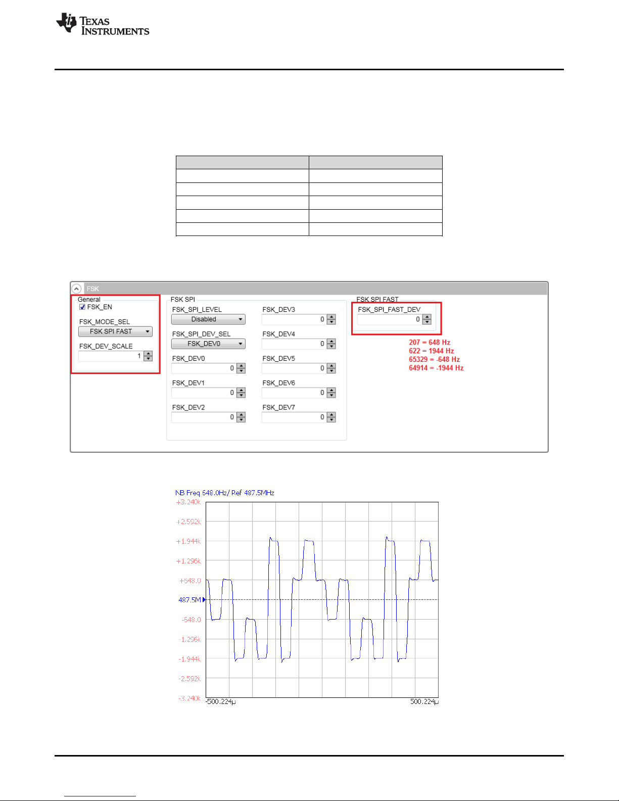
Direct digital FSK modulation is supported in LMX2572. FSK SPI mode supports discrete 2-, 4-, or 8-level
FSK modulation while FSK SPI FAST mode supports arbitrary level FSK modulation. The followings is an
FSK SPI FAST mode example.
Keep writing to the FSK_SPI_FAST_DEV register field the correct values, the output of LMX2572 is a
discrete 4-level FSK modulation signal.
Typical Measurement
Table 5. FSK SPI FAST Mode Example
PARAMETER EXAMPLE VALUE
Phase detector frequency 100 MHz
CHDIV 8
PLL_DEN 8000000
FSK_DEV_SCALE 1
Frequency deviation ±648 Hz; ±1944 Hz
Figure 15. FSK SPI FAST Mode Setting
Figure 16. FSK SPI FAST Mode
SNAU217A–August 2017–Revised November 2017
Submit Documentation Feedback
Copyright © 2017, Texas Instruments Incorporated
LMX2572EVM Evaluation Instructions
11
Page 12
Typical Measurement
3.2.6 Register Readback
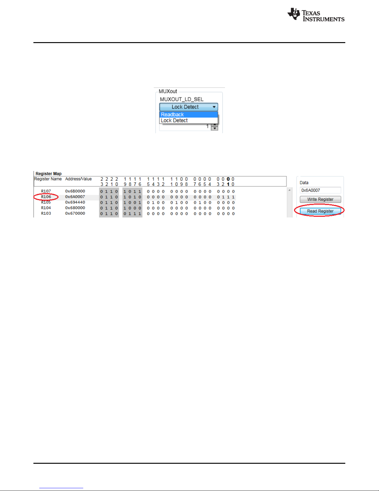
To read back the written register values,
1. Set MUXout_SW Switch 2 to Break position. See Section 2.7.1 for details.
2. In TICS Pro, set MUXOUT_LD_SEL to Readback.
3. Click on the Register Name that you want to read back.
4. Click the Read Register button to read back the register value.
www.ti.com
Figure 17. Readback Setting
Figure 18. Register Readback
12
LMX2572EVM Evaluation Instructions
SNAU217A–August 2017–Revised November 2017
Copyright © 2017, Texas Instruments Incorporated
Submit Documentation Feedback
Page 13
www.ti.com
Schematic
13
SNAU217A–August 2017–Revised November 2017
Submit Documentation Feedback
Copyright © 2017, Texas Instruments Incorporated
LMX2572EVM Evaluation Instructions
4 Schematic
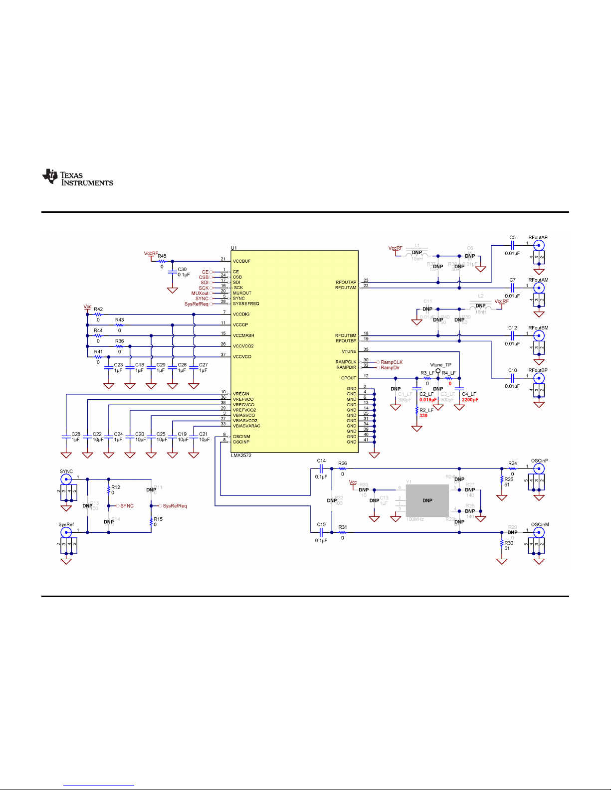
Figure 19. LMX2572EVM Schematic (Page 1)
Page 14
Schematic
www.ti.com
14
SNAU217A–August 2017–Revised November 2017
Submit Documentation Feedback
Copyright © 2017, Texas Instruments Incorporated
LMX2572EVM Evaluation Instructions
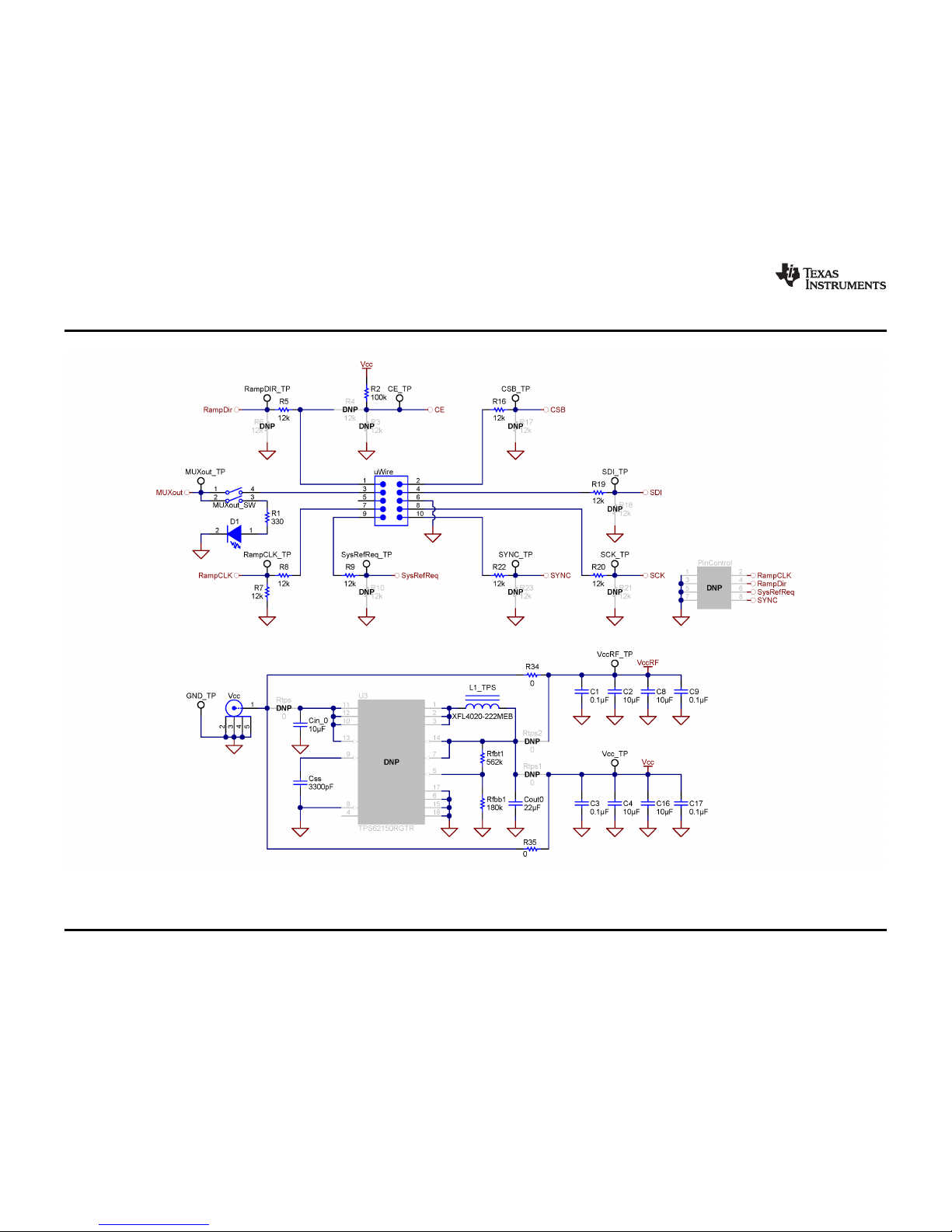
Figure 20. LMX2572EVM Schematic (Page 2)
Page 15
Top layer
RO4003 (Er = 3.38)
16 mil
GND layer
FR4 (Er = 4.6)
Power layer
FR4 (Er = 4.6)
Bottom layer
62 mil
www.ti.com
5 PCB Layout and Layer Stack-up
5.1 PCB Layer Stack-up
The top layer is 1-oz. copper.
Figure 21. PCB Layer Stack-Up
5.2 PCB Layout
PCB Layout and Layer Stack-up
SNAU217A–August 2017–Revised November 2017
Submit Documentation Feedback
Figure 22. Top Layer
Copyright © 2017, Texas Instruments Incorporated
LMX2572EVM Evaluation Instructions
15
Page 16
PCB Layout and Layer Stack-up
www.ti.com
Figure 23. GND Layer
16
LMX2572EVM Evaluation Instructions
Figure 24. Power Layer
SNAU217A–August 2017–Revised November 2017
Copyright © 2017, Texas Instruments Incorporated
Submit Documentation Feedback
Page 17
www.ti.com
PCB Layout and Layer Stack-up
Figure 25. Bottom Layer
SNAU217A–August 2017–Revised November 2017
Submit Documentation Feedback
Copyright © 2017, Texas Instruments Incorporated
LMX2572EVM Evaluation Instructions
17
Page 18
Bill of Materials
6 Bill of Materials
DESIGNATOR QUANTITY DESCRIPTION PART NUMBER MANUFACTURER
C1, C3, C9, C14, C15, C17, C30 7 CAP, CERM, 0.1 µF, 16 V, ±5%, X7R,
C2, C4, C8, C16 4 CAP, CERM, 10 µF, 10 V, ±10%, X5R,
C2_LF 1 CAP, CERM, 0.015 µF, 50 V, ±10%,
C4_LF 1 CAP, CERM, 2200 pF, 50 V, ±5%,
C5, C7, C10, C12 4 CAP, CERM, 0.01 µF, 16 V, ±10%, X7R,
C18, C23, C24, C26, C27, C28, C29 7 CAP, CERM, 1 µF, 16 V, ±10%, X7R,
C19, C20, C21, C22, C25 5 CAP, CERM, 10 µF, 10 V, ±20%, X5R,
CE_TP, CSB_TP, GND_TP,
MUXout_TP, RampCLK_TP,
RampDIR_TP, SCK_TP, SDI_TP,
SYNC_TP, SysRefReq_TP, Vcc_TP,
VccRF_TP, Vtune_TP
Cin_0 1 CAP, CERM, 10 µF, 25 V, ±10%, X5R,
Cout0 1 CAP, CERM, 22 µF, 16 V, ±10%, X5R,
Css 1 CAP, CERM, 3300 pF, 50 V, ±5%,
D1 1 LED, Green, SMD LTST-C190GKT Lite-On
L1_TPS 1 Inductor, Shielded, Composite, 2.2 µH,
MUXout_SW 1 Switch, SPST, Slide, Off-On, 2 Pos, 0.1
OSCinM, OSCinP, SYNC, SysRef, Vcc 5 Connector, SMT, End launch SMA 50 Ω 142-0701-851 Emerson Network
R1 1 RES, 330 Ω, 5%, 0.1 W, 0603 RC0603JR-07330RL Yageo America
R2 1 RES, 100 kΩ, 5%, 0.1 W, 0603 CRCW0603100KJNEA Vishay-Dale
R2_LF 1 RES, 330 Ω, 5%, 0.1 W, 0603 CRCW0603330RJNEA Vishay-Dale
R3_LF, R4_LF, R12, R15, R24, R26,
R31
R5, R7, R8, R9, R16, R19, R20, R22 8 RES, 12 kΩ, 5%, 0.1 W, 0603 CRCW060312K0JNEA Vishay-Dale
R25, R30 2 RES, 51 Ω, 5%, 0.1 W, 0603 CRCW060351R0JNEA Vishay-Dale
R34, R35, R36, R41, R42, R43, R44,
R45
Rfbb1 1 RES, 180 kΩ, 0.1%, 0.1 W, 0603 RT0603BRD07180KL Yageo America
Rfbt1 1 RES, 562 kΩ, 1%, 0.1 W, 0603 CRCW0603562KFKEA Vishay-Dale
RFoutAM, RFoutAP, RFoutBM, RFoutBP 4 JACK, SMA, 50 Ω, Gold, Edge Mount 142-0771-831 Johnson
U1 1 High Performance, Wideband PLLatinum
uWire 1 Header (shrouded), 100 mil, 5x2, Gold
www.ti.com
Table 6. Bill of Materials
0603
0805
X7R, 0603
C0G/NP0, 0603
0402
0603
0603
13 Test Point, Compact, White, TH 5007 Keystone
0805
0805
C0G/NP0, 0603
3.7 A, 0.02 Ω, SMD
A, 20 V, SMD
7 RES, 0 Ω, 5%, 0.1 W, 0603 CRCW06030000Z0EA Vishay-Dale
8 RES, 0 Ω, 5%, 0.1 W, 0603 CRCW06030000Z0EA Vishay-Dale
RF Synthesizer
plated, SMD
0603YC104JAT2A AVX
C0805C106K8PACTU Kemet
GRM188R71H153KA01D MuRata
GRM1885C1H222JA01D MuRata
520L103KT16T AT Ceramics
C1608X7R1C105K080AC TDK
C1608X5R1A106M080AC TDK
GRM219R61E106KA12D MuRata
C2012X5R1C226K125AC TDK
GRM1885C1H332JA01D MuRata
XFL4020-222MEB Coilcraft
219-2MST CTS
Electrocomponents
Power Connectivity
LMX2572RHAR Texas Instruments
52601-S10-8LF FCI
18
LMX2572EVM Evaluation Instructions
SNAU217A–August 2017–Revised November 2017
Copyright © 2017, Texas Instruments Incorporated
Submit Documentation Feedback
Page 19
Device locked
Congratulation!
Start
Yes
Verify hardware setup:
x Validate power supply is connected, turned on, and current limit is appropriate for the device.
x Validate OSCin signal is supplied and turned on, if required.
x Ensure programming cable is hooked up to the board.
x Ensure spectrum analyzer center frequency matches target frequency. Choose wide span so that the carrier can
be seen if it is off frequency.
x Ensure device is not powered down by the CE pin.
x Load all registers (Ctrl+L).
Device locked
Congratulation!
No
Yes
Verify software setup:
x 5HYHUWWRGHIDXOWPRGHLQWKHVRIWZDUHXQGHU³'HIDXOW&RQILJXUDWLRQ´.
x Validate that no boxes are red. If so, mouse over and read the tool tips.
x Ensure that all the frequency boxes values are correct. Also understand that the VCO frequency could be
different than the output frequency as there are often dividers after the boxes.
x Load all registers (Ctrl+L).
x Try Readback at this point, if necessary.
Device locked
Congratulation!
No
Yes
Verify communications:
x *RWR³86%&RPPXQLFDWLRQV´, ³,QWHUIDFH´, ensure that the USB2ANY button is turned green. &OLFN³,GHQWLI\´WR
have the program blink the green LED.
x Send simple one way communication to the device such as: POWERDOWN, RESET, or change the status of a
pin. Realize that if a RESET is done, do a Ctrl+L to refresh the registers afterwards. For POWERDOWN, you can
validate this looking at the current on the power supply.
Device locked
Congratulation!
No
Yes
No
Contact TI support
www.ti.com/support
www.ti.com
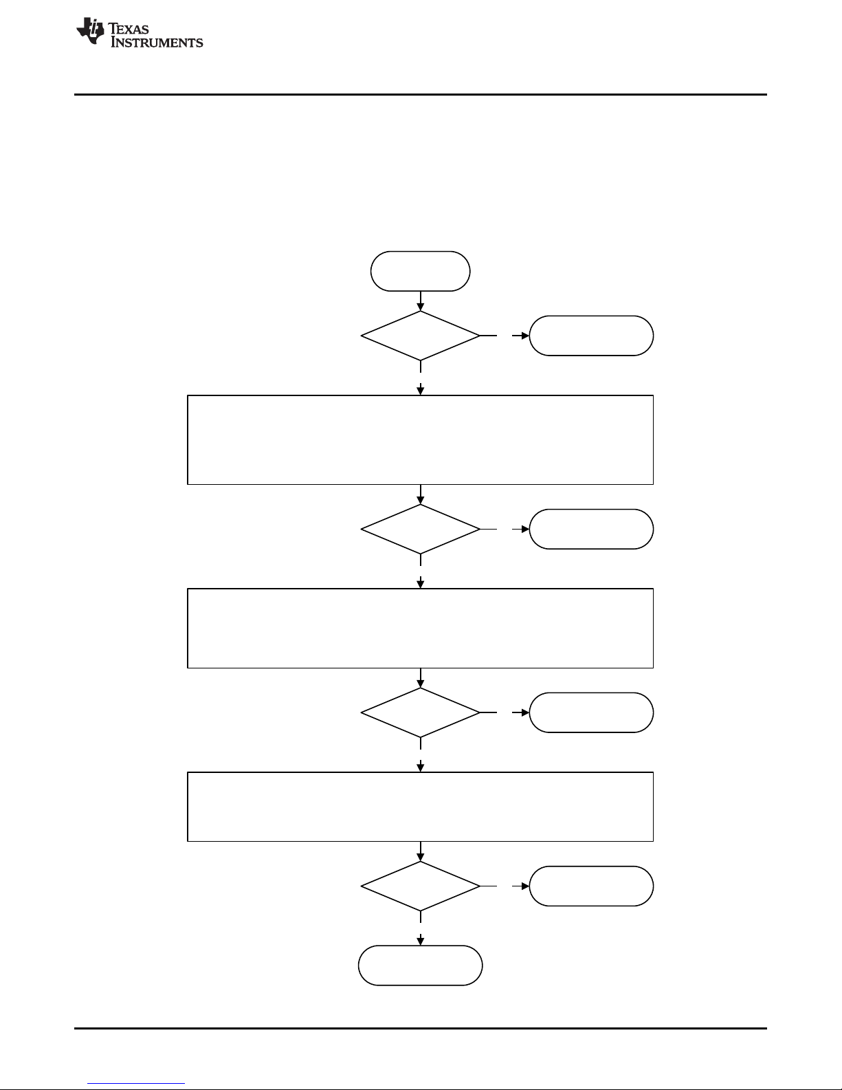
7 Troubleshooting Guide
If the EVM does not work as expected, use the following chart to identify potential root causes. Couples of
thing to note:
• Make modifications to the EVM or change the default settings until AFTER it is verified to be working.
• Register readback requires the correct hardware and software setup. See Section 3.2.6 for details.
• The POR current of the LMX2572EVM is approximately 30 mA.
• The powerdown current of the LMX2572EVM is approximately 2.5 mA.
Troubleshooting Guide
Figure 26. Troubleshooting Guide
SNAU217A–August 2017–Revised November 2017
Submit Documentation Feedback
Copyright © 2017, Texas Instruments Incorporated
LMX2572EVM Evaluation Instructions
19
Page 20
Appendix A
SNAU217A–August 2017–Revised November 2017
Using Different Reference Clock
There are different options to provide a reference clock to LMX2572EVM. By default, the EVM is
configured for an external single-ended clock.
Table 7. Reference Clock Input Configuration
INPUT EXTERNAL CLOCK CRYSTAL OSCILLATOR
Single-
ended
Differential
(LVDS)
20
Using Different Reference Clock
SNAU217A–August 2017–Revised November 2017
Copyright © 2017, Texas Instruments Incorporated
Submit Documentation Feedback
Page 21
Appendix B
SNAU217A–August 2017–Revised November 2017
Reference PRO
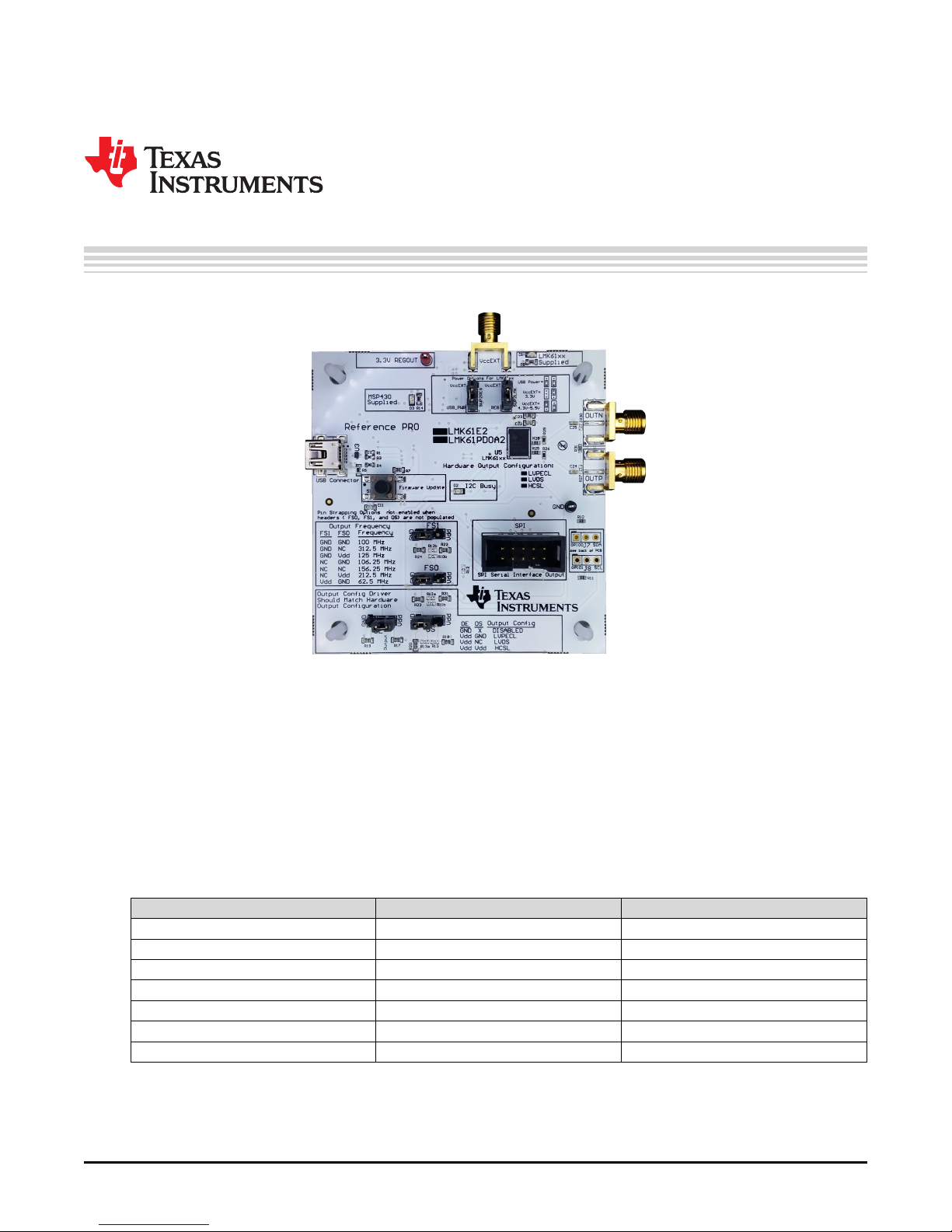
The Reference PRO board is used to program the LMX2572EVM and at the same time, provide a clean
reference clock to LMX2572EVM. The board has several control pins dedicated for control of output
format, output frequency, and output enable control. These control pins are configurable through the
jumpers by strapping the center pin to Vdd position or GND position. Connections from the Vdd position to
the device supply or from the GND position to the ground plane are connected by 1.5-kΩ resistors. By
default, the board is configured for 100-MHz LVPECL output. The power supply to Reference PRO is
obtained from the PC that is connecting to Reference PRO through the USB interface.
B.1 Output Frequency Selection
Jumpers FS1 and FS0 are used to set the output frequency.
Table 8. Reference PRO Output Frequency Selection
FS1 FS0 OUTPUT FREQUENCY (MHz)
GND GND 100
GND NC 312.5
GND Vdd 125
NC GND 106.25
NC NC 156.25
NC Vdd 212.5
Vdd GND 62.5
SNAU217A–August 2017–Revised November 2017
Submit Documentation Feedback
Copyright © 2017, Texas Instruments Incorporated
Reference PRO
21
Page 22
Output Format Selection
B.2 Output Format Selection
The OE pin is used to enable or disable the output.
The OS pin is used to bias internal drivers and change the output format.
Table 9. Reference PRO Output Format Selection
OE OS OUTPUT FORMAT
GND Don't Care Disabled
Vdd GND LVPECL
Vdd NC LVDS
Vdd Vdd HCSL
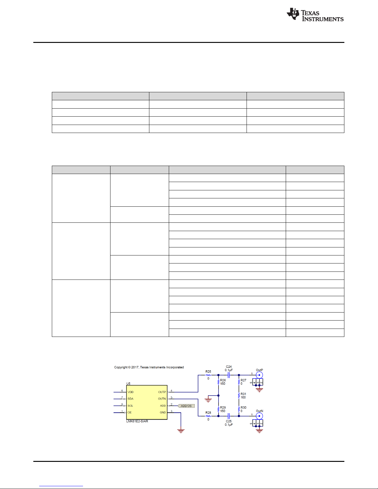
It is imperative to match the output termination passive components as shown inTable 10.
OUTPUT FORMAT COUPLING COMPONENT VALUE
AC (Default
LVPECL
(2)
LVDS
HCSL
(1)
50-Ω to VCC– 2-V termination is required on receiver.
(2)
100-Ω differential termination (R31) is provided onboard. Removing this termination is possible if the differential termination is
available on the receiver.
configuration)
Table 10. Output Termination Configuration
R15, R28 0 Ω
R26, R29 150 Ω
C24, C25 0.01 µF
R27, R30, R31 DNP
DC
AC
DC
AC
DC
(1)
R15, R28, C24, C25 0 Ω
R26, R27, R29, R30, R31 DNP
R25, R27, R28, R30 0 Ω
R31 100 Ω
C24, C25 0.01 µF
R26, R29 DNP
R25, R27, R28, R30, C24, C25 0 Ω
R31 100 Ω
R26, R29 DNP
R25, R28 0 Ω
R26, R29 50 Ω
C24, C25 0.01 µF
R27, R30, R31 DNP
R25, R28, C24, C25 0 Ω
R26, R29 50 Ω
R27, R30, R31 DNP
www.ti.com
22
Reference PRO
Figure 27. Output Termination Schematic
SNAU217A–August 2017–Revised November 2017
Copyright © 2017, Texas Instruments Incorporated
Submit Documentation Feedback
Page 23
www.ti.com
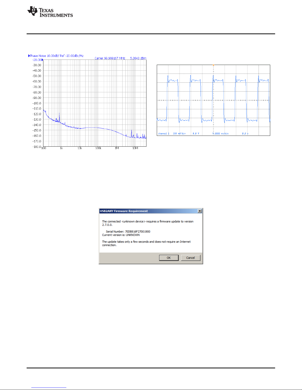
B.3 Typical Output Characteristics
Figure 28. Default Output Phase Nosie Figure 29. Default Output Waveform
B.4 Firmware Update
Usually when the Reference PRO board is used at the first time, TICS Pro will request for a firmware
update. Simply follow the pop-up instructions to complete the update. This is necessary to ensure that the
USB connection between the PC and the Reference PRO board is properly setup, otherwise the
programming to LMX2572EVM will not be successful.
1. When you see this message, click the "OK" button.
Typical Output Characteristics
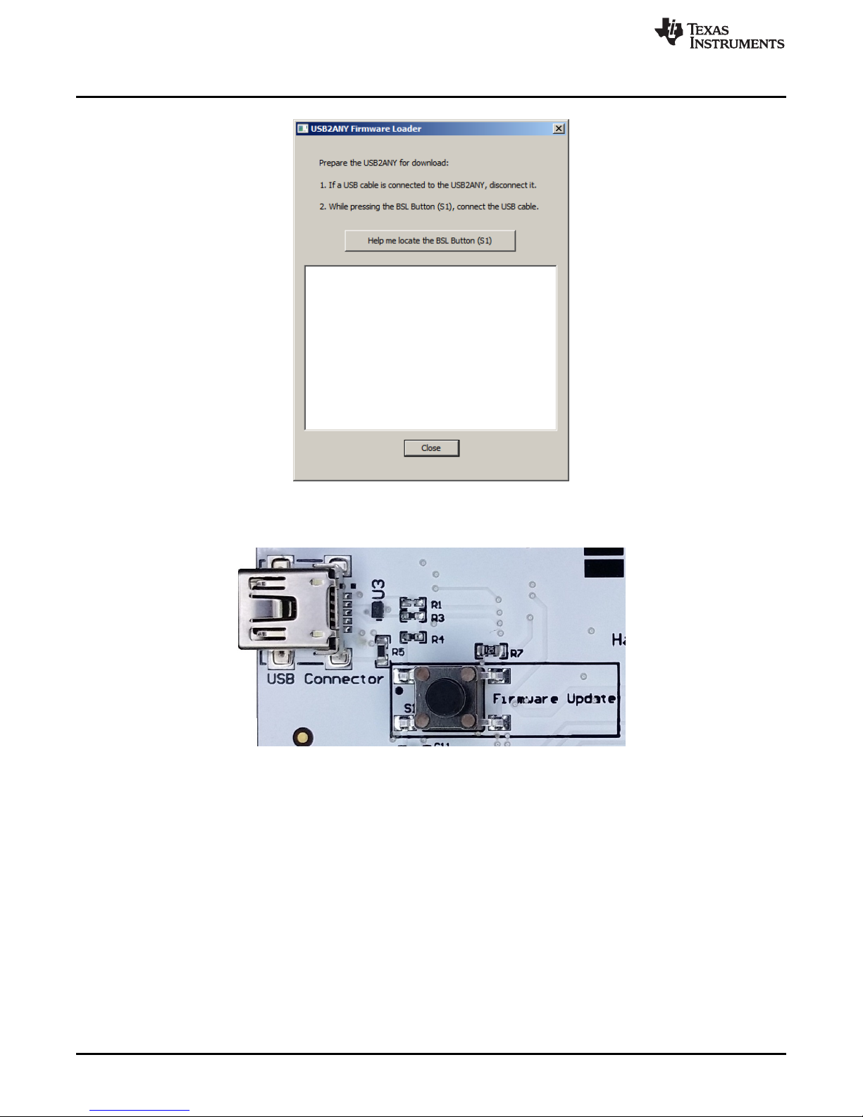
2. Next, follow the on-screen procedure.
SNAU217A–August 2017–Revised November 2017
Submit Documentation Feedback
Figure 30. Firmware Requirement
Copyright © 2017, Texas Instruments Incorporated
Reference PRO
23
Page 24
Firmware Update
www.ti.com
Figure 31. Firmware Loader
3. The BSL button is located next to the USB connector.
Figure 32. BSL Button
4. Follow the on-screen procedure until the below screen is pop-up.
24
Reference PRO
SNAU217A–August 2017–Revised November 2017
Copyright © 2017, Texas Instruments Incorporated
Submit Documentation Feedback
Page 25

www.ti.com
Firmware Update
Figure 33. Update Firmware
5. Click the "Upgrade Firmware" button, the firmware will be upgrading. Click the "Close" button after it is
done.
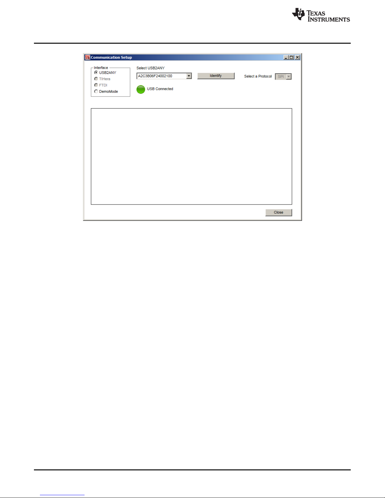
6. Check the USB connection in TICS Pro by clicking USB communications → Interface. Make sure the
USB Connected button is turned green.
SNAU217A–August 2017–Revised November 2017
Submit Documentation Feedback
Figure 34. Firmware Update Completed
Copyright © 2017, Texas Instruments Incorporated
Reference PRO
25
Page 26
Firmware Update
www.ti.com
Figure 35. USB Communications
26
Reference PRO
SNAU217A–August 2017–Revised November 2017
Copyright © 2017, Texas Instruments Incorporated
Submit Documentation Feedback
Page 27

www.ti.com
Revision History
Revision History
NOTE: Page numbers for previous revisions may differ from page numbers in the current version.
Changes from Original (August 2017) to A Revision ..................................................................................................... Page
• Added phase adjustment example...................................................................................................... 6
• Added calibration-free ramping example............................................................................................... 7
• Added automatic ramp example ........................................................................................................ 9
• Added SYSREF example............................................................................................................... 10
• Added FSK modulation example ...................................................................................................... 11
• Added register readback example..................................................................................................... 12
• Added troubleshooting guide........................................................................................................... 19
• Changed the graphic of single-ended input with crystal oscillator ................................................................ 20
SNAU217A–August 2017–Revised November 2017
Submit Documentation Feedback
Copyright © 2017, Texas Instruments Incorporated
Revision History
27
Page 28

STANDARD TERMS FOR EVALUATION MODULES
1. Delivery: TI delivers TI evaluation boards, kits, or modules, including any accompanying demonstration software, components, and/or
documentation which may be provided together or separately (collectively, an “EVM” or “EVMs”) to the User (“User”) in accordance
with the terms set forth herein. User's acceptance of the EVM is expressly subject to the following terms.
1.1 EVMs are intended solely for product or software developers for use in a research and development setting to facilitate feasibility
evaluation, experimentation, or scientific analysis of TI semiconductors products. EVMs have no direct function and are not
finished products. EVMs shall not be directly or indirectly assembled as a part or subassembly in any finished product. For
clarification, any software or software tools provided with the EVM (“Software”) shall not be subject to the terms and conditions
set forth herein but rather shall be subject to the applicable terms that accompany such Software
1.2 EVMs are not intended for consumer or household use. EVMs may not be sold, sublicensed, leased, rented, loaned, assigned,
or otherwise distributed for commercial purposes by Users, in whole or in part, or used in any finished product or production
system.
2 Limited Warranty and Related Remedies/Disclaimers:
2.1 These terms do not apply to Software. The warranty, if any, for Software is covered in the applicable Software License
Agreement.
2.2 TI warrants that the TI EVM will conform to TI's published specifications for ninety (90) days after the date TI delivers such EVM
to User. Notwithstanding the foregoing, TI shall not be liable for a nonconforming EVM if (a) the nonconformity was caused by
neglect, misuse or mistreatment by an entity other than TI, including improper installation or testing, or for any EVMs that have
been altered or modified in any way by an entity other than TI, (b) the nonconformity resulted from User's design, specifications
or instructions for such EVMs or improper system design, or (c) User has not paid on time. Testing and other quality control
techniques are used to the extent TI deems necessary. TI does not test all parameters of each EVM.
User's claims against TI under this Section 2 are void if User fails to notify TI of any apparent defects in the EVMs within ten (10)
business days after delivery, or of any hidden defects with ten (10) business days after the defect has been detected.
2.3 TI's sole liability shall be at its option to repair or replace EVMs that fail to conform to the warranty set forth above, or credit
User's account for such EVM. TI's liability under this warranty shall be limited to EVMs that are returned during the warranty
period to the address designated by TI and that are determined by TI not to conform to such warranty. If TI elects to repair or
replace such EVM, TI shall have a reasonable time to repair such EVM or provide replacements. Repaired EVMs shall be
warranted for the remainder of the original warranty period. Replaced EVMs shall be warranted for a new full ninety (90) day
warranty period.
3 Regulatory Notices:
3.1 United States
3.1.1 Notice applicable to EVMs not FCC-Approved:
FCC NOTICE: This kit is designed to allow product developers to evaluate electronic components, circuitry, or software
associated with the kit to determine whether to incorporate such items in a finished product and software developers to write
software applications for use with the end product. This kit is not a finished product and when assembled may not be resold or
otherwise marketed unless all required FCC equipment authorizations are first obtained. Operation is subject to the condition
that this product not cause harmful interference to licensed radio stations and that this product accept harmful interference.
Unless the assembled kit is designed to operate under part 15, part 18 or part 95 of this chapter, the operator of the kit must
operate under the authority of an FCC license holder or must secure an experimental authorization under part 5 of this chapter.
3.1.2 For EVMs annotated as FCC – FEDERAL COMMUNICATIONS COMMISSION Part 15 Compliant:
CAUTION
This device complies with part 15 of the FCC Rules. Operation is subject to the following two conditions: (1) This device may not
cause harmful interference, and (2) this device must accept any interference received, including interference that may cause
undesired operation.
Changes or modifications not expressly approved by the party responsible for compliance could void the user's authority to
operate the equipment.
FCC Interference Statement for Class A EVM devices
NOTE: This equipment has been tested and found to comply with the limits for a Class A digital device, pursuant to part 15 of
the FCC Rules. These limits are designed to provide reasonable protection against harmful interference when the equipment is
operated in a commercial environment. This equipment generates, uses, and can radiate radio frequency energy and, if not
installed and used in accordance with the instruction manual, may cause harmful interference to radio communications.
Operation of this equipment in a residential area is likely to cause harmful interference in which case the user will be required to
correct the interference at his own expense.
Page 29

FCC Interference Statement for Class B EVM devices
NOTE: This equipment has been tested and found to comply with the limits for a Class B digital device, pursuant to part 15 of
the FCC Rules. These limits are designed to provide reasonable protection against harmful interference in a residential
installation. This equipment generates, uses and can radiate radio frequency energy and, if not installed and used in accordance
with the instructions, may cause harmful interference to radio communications. However, there is no guarantee that interference
will not occur in a particular installation. If this equipment does cause harmful interference to radio or television reception, which
can be determined by turning the equipment off and on, the user is encouraged to try to correct the interference by one or more
of the following measures:
• Reorient or relocate the receiving antenna.
• Increase the separation between the equipment and receiver.
• Connect the equipment into an outlet on a circuit different from that to which the receiver is connected.
• Consult the dealer or an experienced radio/TV technician for help.
3.2 Canada
3.2.1 For EVMs issued with an Industry Canada Certificate of Conformance to RSS-210 or RSS-247
Concerning EVMs Including Radio Transmitters:
This device complies with Industry Canada license-exempt RSSs. Operation is subject to the following two conditions:
(1) this device may not cause interference, and (2) this device must accept any interference, including interference that may
cause undesired operation of the device.
Concernant les EVMs avec appareils radio:
Le présent appareil est conforme aux CNR d'Industrie Canada applicables aux appareils radio exempts de licence. L'exploitation
est autorisée aux deux conditions suivantes: (1) l'appareil ne doit pas produire de brouillage, et (2) l'utilisateur de l'appareil doit
accepter tout brouillage radioélectrique subi, même si le brouillage est susceptible d'en compromettre le fonctionnement.
Concerning EVMs Including Detachable Antennas:
Under Industry Canada regulations, this radio transmitter may only operate using an antenna of a type and maximum (or lesser)
gain approved for the transmitter by Industry Canada. To reduce potential radio interference to other users, the antenna type
and its gain should be so chosen that the equivalent isotropically radiated power (e.i.r.p.) is not more than that necessary for
successful communication. This radio transmitter has been approved by Industry Canada to operate with the antenna types
listed in the user guide with the maximum permissible gain and required antenna impedance for each antenna type indicated.
Antenna types not included in this list, having a gain greater than the maximum gain indicated for that type, are strictly prohibited
for use with this device.
Concernant les EVMs avec antennes détachables
Conformément à la réglementation d'Industrie Canada, le présent émetteur radio peut fonctionner avec une antenne d'un type et
d'un gain maximal (ou inférieur) approuvé pour l'émetteur par Industrie Canada. Dans le but de réduire les risques de brouillage
radioélectrique à l'intention des autres utilisateurs, il faut choisir le type d'antenne et son gain de sorte que la puissance isotrope
rayonnée équivalente (p.i.r.e.) ne dépasse pas l'intensité nécessaire à l'établissement d'une communication satisfaisante. Le
présent émetteur radio a été approuvé par Industrie Canada pour fonctionner avec les types d'antenne énumérés dans le
manuel d’usage et ayant un gain admissible maximal et l'impédance requise pour chaque type d'antenne. Les types d'antenne
non inclus dans cette liste, ou dont le gain est supérieur au gain maximal indiqué, sont strictement interdits pour l'exploitation de
l'émetteur
3.3 Japan
3.3.1 Notice for EVMs delivered in Japan: Please see http://www.tij.co.jp/lsds/ti_ja/general/eStore/notice_01.page 日本国内に
輸入される評価用キット、ボードについては、次のところをご覧ください。
http://www.tij.co.jp/lsds/ti_ja/general/eStore/notice_01.page
3.3.2 Notice for Users of EVMs Considered “Radio Frequency Products” in Japan: EVMs entering Japan may not be certified
by TI as conforming to Technical Regulations of Radio Law of Japan.
If User uses EVMs in Japan, not certified to Technical Regulations of Radio Law of Japan, User is required to follow the
instructions set forth by Radio Law of Japan, which includes, but is not limited to, the instructions below with respect to EVMs
(which for the avoidance of doubt are stated strictly for convenience and should be verified by User):
1. Use EVMs in a shielded room or any other test facility as defined in the notification #173 issued by Ministry of Internal
Affairs and Communications on March 28, 2006, based on Sub-section 1.1 of Article 6 of the Ministry’s Rule for
Enforcement of Radio Law of Japan,
2. Use EVMs only after User obtains the license of Test Radio Station as provided in Radio Law of Japan with respect to
EVMs, or
3. Use of EVMs only after User obtains the Technical Regulations Conformity Certification as provided in Radio Law of Japan
with respect to EVMs. Also, do not transfer EVMs, unless User gives the same notice above to the transferee. Please note
that if User does not follow the instructions above, User will be subject to penalties of Radio Law of Japan.
Page 30

【無線電波を送信する製品の開発キットをお使いになる際の注意事項】 開発キットの中には技術基準適合証明を受けて
いないものがあります。 技術適合証明を受けていないもののご使用に際しては、電波法遵守のため、以下のいずれかの
措置を取っていただく必要がありますのでご注意ください。
1. 電波法施行規則第6条第1項第1号に基づく平成18年3月28日総務省告示第173号で定められた電波暗室等の試験設備でご使用
いただく。
2. 実験局の免許を取得後ご使用いただく。
3. 技術基準適合証明を取得後ご使用いただく。
なお、本製品は、上記の「ご使用にあたっての注意」を譲渡先、移転先に通知しない限り、譲渡、移転できないものとします。
上記を遵守頂けない場合は、電波法の罰則が適用される可能性があることをご留意ください。 日本テキサス・イ
ンスツルメンツ株式会社
東京都新宿区西新宿6丁目24番1号
西新宿三井ビル
3.3.3 Notice for EVMs for Power Line Communication: Please see http://www.tij.co.jp/lsds/ti_ja/general/eStore/notice_02.page
電力線搬送波通信についての開発キットをお使いになる際の注意事項については、次のところをご覧ください。http:/
/www.tij.co.jp/lsds/ti_ja/general/eStore/notice_02.page
3.4 European Union
3.4.1 For EVMs subject to EU Directive 2014/30/EU (Electromagnetic Compatibility Directive):
This is a class A product intended for use in environments other than domestic environments that are connected to a
low-voltage power-supply network that supplies buildings used for domestic purposes. In a domestic environment this
product may cause radio interference in which case the user may be required to take adequate measures.
4 EVM Use Restrictions and Warnings:
4.1 EVMS ARE NOT FOR USE IN FUNCTIONAL SAFETY AND/OR SAFETY CRITICAL EVALUATIONS, INCLUDING BUT NOT
LIMITED TO EVALUATIONS OF LIFE SUPPORT APPLICATIONS.
4.2 User must read and apply the user guide and other available documentation provided by TI regarding the EVM prior to handling
or using the EVM, including without limitation any warning or restriction notices. The notices contain important safety information
related to, for example, temperatures and voltages.
4.3 Safety-Related Warnings and Restrictions:
4.3.1 User shall operate the EVM within TI’s recommended specifications and environmental considerations stated in the user
guide, other available documentation provided by TI, and any other applicable requirements and employ reasonable and
customary safeguards. Exceeding the specified performance ratings and specifications (including but not limited to input
and output voltage, current, power, and environmental ranges) for the EVM may cause personal injury or death, or
property damage. If there are questions concerning performance ratings and specifications, User should contact a TI
field representative prior to connecting interface electronics including input power and intended loads. Any loads applied
outside of the specified output range may also result in unintended and/or inaccurate operation and/or possible
permanent damage to the EVM and/or interface electronics. Please consult the EVM user guide prior to connecting any
load to the EVM output. If there is uncertainty as to the load specification, please contact a TI field representative.
During normal operation, even with the inputs and outputs kept within the specified allowable ranges, some circuit
components may have elevated case temperatures. These components include but are not limited to linear regulators,
switching transistors, pass transistors, current sense resistors, and heat sinks, which can be identified using the
information in the associated documentation. When working with the EVM, please be aware that the EVM may become
very warm.
4.3.2 EVMs are intended solely for use by technically qualified, professional electronics experts who are familiar with the
dangers and application risks associated with handling electrical mechanical components, systems, and subsystems.
User assumes all responsibility and liability for proper and safe handling and use of the EVM by User or its employees,
affiliates, contractors or designees. User assumes all responsibility and liability to ensure that any interfaces (electronic
and/or mechanical) between the EVM and any human body are designed with suitable isolation and means to safely
limit accessible leakage currents to minimize the risk of electrical shock hazard. User assumes all responsibility and
liability for any improper or unsafe handling or use of the EVM by User or its employees, affiliates, contractors or
designees.
4.4 User assumes all responsibility and liability to determine whether the EVM is subject to any applicable international, federal,
state, or local laws and regulations related to User’s handling and use of the EVM and, if applicable, User assumes all
responsibility and liability for compliance in all respects with such laws and regulations. User assumes all responsibility and
liability for proper disposal and recycling of the EVM consistent with all applicable international, federal, state, and local
requirements.
5. Accuracy of Information: To the extent TI provides information on the availability and function of EVMs, TI attempts to be as accurate
as possible. However, TI does not warrant the accuracy of EVM descriptions, EVM availability or other information on its websites as
accurate, complete, reliable, current, or error-free.
Page 31

6. Disclaimers:
6.1 EXCEPT AS SET FORTH ABOVE, EVMS AND ANY MATERIALS PROVIDED WITH THE EVM (INCLUDING, BUT NOT
LIMITED TO, REFERENCE DESIGNS AND THE DESIGN OF THE EVM ITSELF) ARE PROVIDED "AS IS" AND "WITH ALL
FAULTS." TI DISCLAIMS ALL OTHER WARRANTIES, EXPRESS OR IMPLIED, REGARDING SUCH ITEMS, INCLUDING BUT
NOT LIMITED TO ANY EPIDEMIC FAILURE WARRANTY OR IMPLIED WARRANTIES OF MERCHANTABILITY OR FITNESS
FOR A PARTICULAR PURPOSE OR NON-INFRINGEMENT OF ANY THIRD PARTY PATENTS, COPYRIGHTS, TRADE
SECRETS OR OTHER INTELLECTUAL PROPERTY RIGHTS.
6.2 EXCEPT FOR THE LIMITED RIGHT TO USE THE EVM SET FORTH HEREIN, NOTHING IN THESE TERMS SHALL BE
CONSTRUED AS GRANTING OR CONFERRING ANY RIGHTS BY LICENSE, PATENT, OR ANY OTHER INDUSTRIAL OR
INTELLECTUAL PROPERTY RIGHT OF TI, ITS SUPPLIERS/LICENSORS OR ANY OTHER THIRD PARTY, TO USE THE
EVM IN ANY FINISHED END-USER OR READY-TO-USE FINAL PRODUCT, OR FOR ANY INVENTION, DISCOVERY OR
IMPROVEMENT, REGARDLESS OF WHEN MADE, CONCEIVED OR ACQUIRED.
7. USER'S INDEMNITY OBLIGATIONS AND REPRESENTATIONS. USER WILL DEFEND, INDEMNIFY AND HOLD TI, ITS
LICENSORS AND THEIR REPRESENTATIVES HARMLESS FROM AND AGAINST ANY AND ALL CLAIMS, DAMAGES, LOSSES,
EXPENSES, COSTS AND LIABILITIES (COLLECTIVELY, "CLAIMS") ARISING OUT OF OR IN CONNECTION WITH ANY
HANDLING OR USE OF THE EVM THAT IS NOT IN ACCORDANCE WITH THESE TERMS. THIS OBLIGATION SHALL APPLY
WHETHER CLAIMS ARISE UNDER STATUTE, REGULATION, OR THE LAW OF TORT, CONTRACT OR ANY OTHER LEGAL
THEORY, AND EVEN IF THE EVM FAILS TO PERFORM AS DESCRIBED OR EXPECTED.
8. Limitations on Damages and Liability:
8.1 General Limitations. IN NO EVENT SHALL TI BE LIABLE FOR ANY SPECIAL, COLLATERAL, INDIRECT, PUNITIVE,
INCIDENTAL, CONSEQUENTIAL, OR EXEMPLARY DAMAGES IN CONNECTION WITH OR ARISING OUT OF THESE
TERMS OR THE USE OF THE EVMS , REGARDLESS OF WHETHER TI HAS BEEN ADVISED OF THE POSSIBILITY OF
SUCH DAMAGES. EXCLUDED DAMAGES INCLUDE, BUT ARE NOT LIMITED TO, COST OF REMOVAL OR
REINSTALLATION, ANCILLARY COSTS TO THE PROCUREMENT OF SUBSTITUTE GOODS OR SERVICES, RETESTING,
OUTSIDE COMPUTER TIME, LABOR COSTS, LOSS OF GOODWILL, LOSS OF PROFITS, LOSS OF SAVINGS, LOSS OF
USE, LOSS OF DATA, OR BUSINESS INTERRUPTION. NO CLAIM, SUIT OR ACTION SHALL BE BROUGHT AGAINST TI
MORE THAN TWELVE (12) MONTHS AFTER THE EVENT THAT GAVE RISE TO THE CAUSE OF ACTION HAS
OCCURRED.
8.2 Specific Limitations. IN NO EVENT SHALL TI'S AGGREGATE LIABILITY FROM ANY USE OF AN EVM PROVIDED
HEREUNDER, INCLUDING FROM ANY WARRANTY, INDEMITY OR OTHER OBLIGATION ARISING OUT OF OR IN
CONNECTION WITH THESE TERMS, , EXCEED THE TOTAL AMOUNT PAID TO TI BY USER FOR THE PARTICULAR
EVM(S) AT ISSUE DURING THE PRIOR TWELVE (12) MONTHS WITH RESPECT TO WHICH LOSSES OR DAMAGES ARE
CLAIMED. THE EXISTENCE OF MORE THAN ONE CLAIM SHALL NOT ENLARGE OR EXTEND THIS LIMIT.
9. Return Policy. Except as otherwise provided, TI does not offer any refunds, returns, or exchanges. Furthermore, no return of EVM(s)
will be accepted if the package has been opened and no return of the EVM(s) will be accepted if they are damaged or otherwise not in
a resalable condition. If User feels it has been incorrectly charged for the EVM(s) it ordered or that delivery violates the applicable
order, User should contact TI. All refunds will be made in full within thirty (30) working days from the return of the components(s),
excluding any postage or packaging costs.
10. Governing Law: These terms and conditions shall be governed by and interpreted in accordance with the laws of the State of Texas,
without reference to conflict-of-laws principles. User agrees that non-exclusive jurisdiction for any dispute arising out of or relating to
these terms and conditions lies within courts located in the State of Texas and consents to venue in Dallas County, Texas.
Notwithstanding the foregoing, any judgment may be enforced in any United States or foreign court, and TI may seek injunctive relief
in any United States or foreign court.
Mailing Address: Texas Instruments, Post Office Box 655303, Dallas, Texas 75265
Copyright © 2017, Texas Instruments Incorporated
Page 32

IMPORTANT NOTICE FOR TI DESIGN INFORMATION AND RESOURCES
Texas Instruments Incorporated (‘TI”) technical, application or other design advice, services or information, including, but not limited to,
reference designs and materials relating to evaluation modules, (collectively, “TI Resources”) are intended to assist designers who are
developing applications that incorporate TI products; by downloading, accessing or using any particular TI Resource in any way, you
(individually or, if you are acting on behalf of a company, your company) agree to use it solely for this purpose and subject to the terms of
this Notice.
TI’s provision of TI Resources does not expand or otherwise alter TI’s applicable published warranties or warranty disclaimers for TI
products, and no additional obligations or liabilities arise from TI providing such TI Resources. TI reserves the right to make corrections,
enhancements, improvements and other changes to its TI Resources.
You understand and agree that you remain responsible for using your independent analysis, evaluation and judgment in designing your
applications and that you have full and exclusive responsibility to assure the safety of your applications and compliance of your applications
(and of all TI products used in or for your applications) with all applicable regulations, laws and other applicable requirements. You
represent that, with respect to your applications, you have all the necessary expertise to create and implement safeguards that (1)
anticipate dangerous consequences of failures, (2) monitor failures and their consequences, and (3) lessen the likelihood of failures that
might cause harm and take appropriate actions. You agree that prior to using or distributing any applications that include TI products, you
will thoroughly test such applications and the functionality of such TI products as used in such applications. TI has not conducted any
testing other than that specifically described in the published documentation for a particular TI Resource.
You are authorized to use, copy and modify any individual TI Resource only in connection with the development of applications that include
the TI product(s) identified in such TI Resource. NO OTHER LICENSE, EXPRESS OR IMPLIED, BY ESTOPPEL OR OTHERWISE TO
ANY OTHER TI INTELLECTUAL PROPERTY RIGHT, AND NO LICENSE TO ANY TECHNOLOGY OR INTELLECTUAL PROPERTY
RIGHT OF TI OR ANY THIRD PARTY IS GRANTED HEREIN, including but not limited to any patent right, copyright, mask work right, or
other intellectual property right relating to any combination, machine, or process in which TI products or services are used. Information
regarding or referencing third-party products or services does not constitute a license to use such products or services, or a warranty or
endorsement thereof. Use of TI Resources may require a license from a third party under the patents or other intellectual property of the
third party, or a license from TI under the patents or other intellectual property of TI.
TI RESOURCES ARE PROVIDED “AS IS” AND WITH ALL FAULTS. TI DISCLAIMS ALL OTHER WARRANTIES OR
REPRESENTATIONS, EXPRESS OR IMPLIED, REGARDING TI RESOURCES OR USE THEREOF, INCLUDING BUT NOT LIMITED TO
ACCURACY OR COMPLETENESS, TITLE, ANY EPIDEMIC FAILURE WARRANTY AND ANY IMPLIED WARRANTIES OF
MERCHANTABILITY, FITNESS FOR A PARTICULAR PURPOSE, AND NON-INFRINGEMENT OF ANY THIRD PARTY INTELLECTUAL
PROPERTY RIGHTS.
TI SHALL NOT BE LIABLE FOR AND SHALL NOT DEFEND OR INDEMNIFY YOU AGAINST ANY CLAIM, INCLUDING BUT NOT
LIMITED TO ANY INFRINGEMENT CLAIM THAT RELATES TO OR IS BASED ON ANY COMBINATION OF PRODUCTS EVEN IF
DESCRIBED IN TI RESOURCES OR OTHERWISE. IN NO EVENT SHALL TI BE LIABLE FOR ANY ACTUAL, DIRECT, SPECIAL,
COLLATERAL, INDIRECT, PUNITIVE, INCIDENTAL, CONSEQUENTIAL OR EXEMPLARY DAMAGES IN CONNECTION WITH OR
ARISING OUT OF TI RESOURCES OR USE THEREOF, AND REGARDLESS OF WHETHER TI HAS BEEN ADVISED OF THE
POSSIBILITY OF SUCH DAMAGES.
You agree to fully indemnify TI and its representatives against any damages, costs, losses, and/or liabilities arising out of your noncompliance with the terms and provisions of this Notice.
This Notice applies to TI Resources. Additional terms apply to the use and purchase of certain types of materials, TI products and services.
These include; without limitation, TI’s standard terms for semiconductor products http://www.ti.com/sc/docs/stdterms.htm), evaluation
modules, and samples (http://www.ti.com/sc/docs/sampterms.htm).
Mailing Address: Texas Instruments, Post Office Box 655303, Dallas, Texas 75265
Copyright © 2017, Texas Instruments Incorporated
 Loading...