

Datasheet LMX2512LQX1065, LMX2512LQX0967, LMX2512LQ1065, LMX25121065EVAL, LMX25120967EVAL Datasheet (NSC)
...Page 1
LMX2502/LMX2512
PLLatinum
™
Frequency Synthesizer System with
Integrated VCO
General Description
LMX2502 and LMX2512 are highly integrated, high performance, low power frequency synthesizer systems optimized
for Korean PCS and Korean Cellular CDMA (1xRTT, IS-95)
mobile handsets. Using a proprietary digital phase locked
loop technique, LMX2502 and LMX2512 generate very
stable, low noise local oscillator signals for up and down
conversion in wireless communications devices.
LMX2502 and LMX2512 include a voltage controlled oscillator (VCO), a loop filter, and a fractional-N RF PLL based on
a delta sigma modulator. In concert these blocks form a
closed loop RF synthesizer system. LMX2502 supports the
Korean PCS band and LMX2512 supports the Korean Cellular band.
LMX2502 and LMX2512 include an Integer-N IF PLL also.
For more flexible loop filter designs, the IF PLL includes a
4-level programmable charge pump. Together with an external VCO and loop filter, LMX2502 and LMX2512 make a
complete closed loop IF synthesizer system.
Serial data is transferred to the device via a three-wire
MICROWIRE interface (DATA, LE, CLK).
Operating supply voltage ranges from 2.7 V to 3.3 V.
LMX2502 and LMX2512 feature low current consumption:
17 mA at 2.8 V.
LMX2502 and LMX2512 are available in a 28-pin leadless
leadframe package (LLP).
Features
n Small Size
5.0 mm X 5.0 mm X 0.75 mm 28-Pin LLP Package
n RF Synthesizer System
Integrated RF VCO
Integrated Loop Filter
Low Spurious, Low Phase Noise Fractional-N RF PLL
Based on 11-Bit Delta Sigma Modulator
10 kHz Frequency Resolution
n IF Synthesizer System
Integer-N IF PLL
Programmable Charge Pump Current Levels
Programmable Frequency
n Supports Various Reference Frequencies
19.20/19.68 MHz
n Fast Lock Time: 500 µs
n Low Current Consumption
17 mA at 2.8 V
n 2.7 V to 3.3 V Operation
n Digital Filtered Lock Detect Output
n Hardware and Software Power Down Control
Applications
n Korean PCS CDMA Systems
n Korean Cellular CDMA Systems
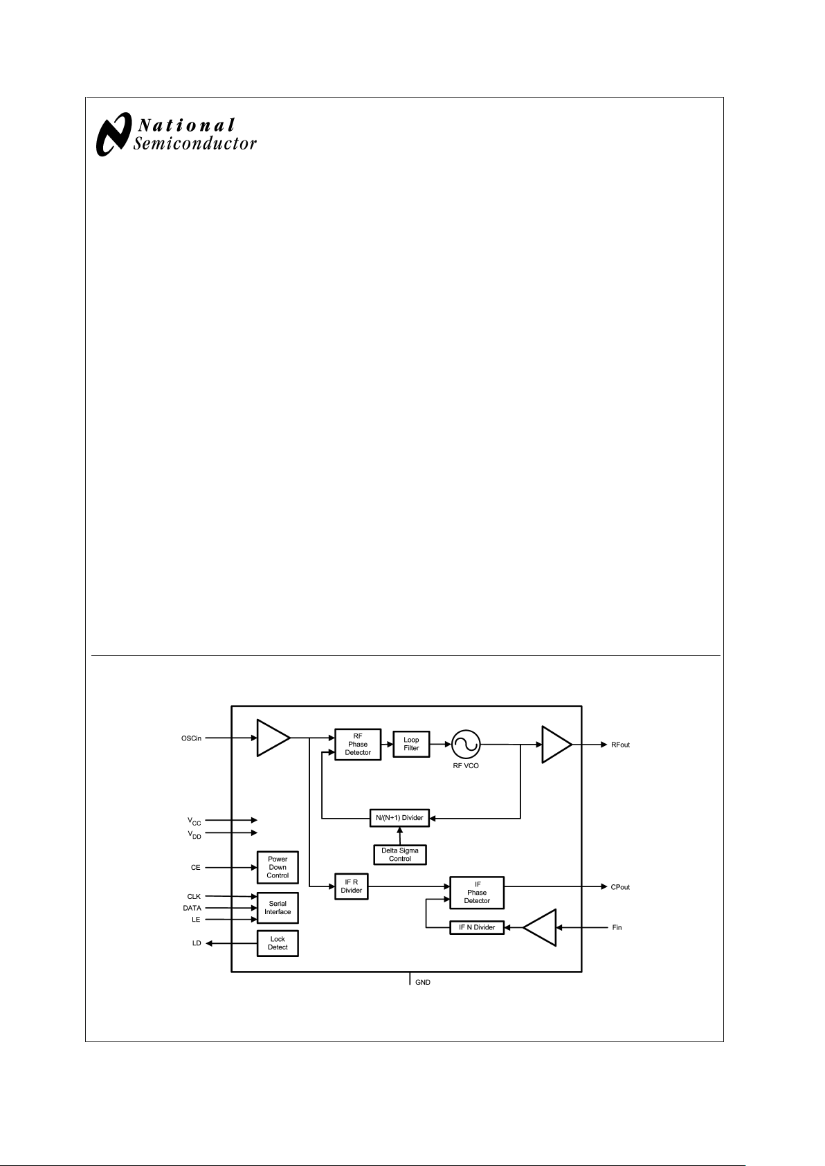
Functional Block Diagram
20068001
PLLatinum™is a trademark of National Semiconductor Corporation.
June 2003
LMX2502/LMX2512 Frequency Synthesizer System with Integrated VCO
© 2003 National Semiconductor Corporation DS200680 www.national.com
Page 2
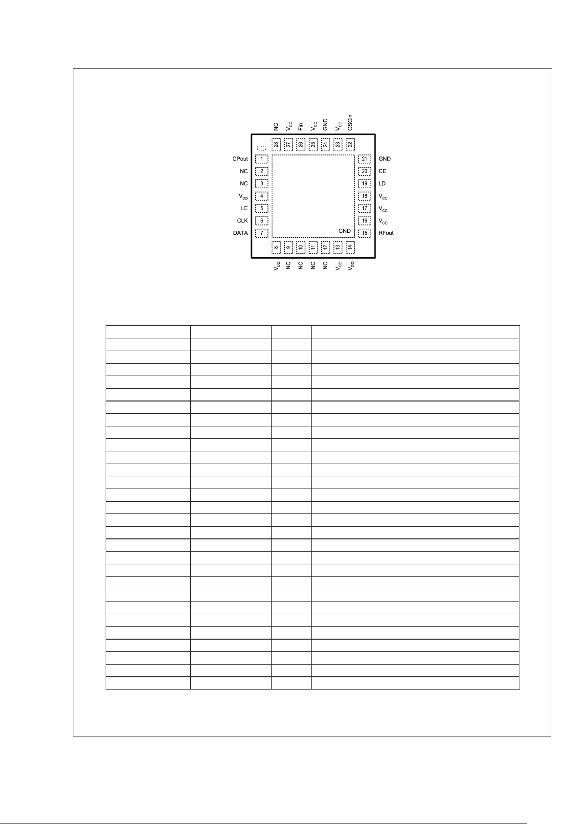
Connection Diagram
28-Pin LLP (LQ) Package
20068002
NOTE: Analog ground connected through exposed die attached pad.
Pin Descriptions
Pin Number Name I/O Description
1 CPout O IF PLL charge pump output
2 NC – Do not connect to any node on the printed circuit board.
3 NC – Do not connect to any node on the printed circuit board.
4V
DD
– Supply voltage for IF analog circuitry
5 LE I MICROWIRE Latch Enable
6 CLK I MICROWIRE Clock
7 DATA I MICROWIRE Data
8V
DD
– Supply voltage for VCO
9 NC – Do not connect to any node on the printed circuit board.
10 NC – Do not connect to any node on the printed circuit board.
11 NC – Do not connect to any node on the printed circuit board.
12 NC – Do not connect to any node on the printed circuit board.
13 V
DD
– Supply voltage for VCO
14 V
DD
– Supply voltage for VCO output buffer
15 RFout O Buffered VCO output
16 V
CC
– Supply voltage for RF prescaler
17 V
CC
– Supply voltage for charge pump
18 V
CC
– Supply voltage for RF digital circuitry
19 LD O Lock Detect
20 CE I Chip Enable control pin
21 GND – Ground for digital circuitry
22 OSCin I Reference frequency input
23 V
CC
– Supply voltage for reference input buffer
24 GND – Ground for digital circuitry
25 V
CC
– Supply voltage for IF digital circuitry
26 Fin I IF buffer/prescaler input
27 V
CC
– Supply voltage for IF buffer/prescaler
28 NC – Do not connect to any node on the printed circuit board.
LMX2502/LMX2512
www.national.com 2
Page 3
Ordering Information
Part Number RF Min.
(MHz)
RF Max.
(MHz)
RF Center
(MHz)
IF
(MHz)
Package
Marking
Supplied As
LMX2502LQX1635 1619.62 1649.62
~
1635 440.76 25021635 4500 units on
tape and reel
LMX2502LQ1635 1619.62 1649.62
~
1635 440.76 25021635 1000 units on
tape and reel
LMX2512LQX0967 954.42 979.35
~
967 170.76 25120967 4500 units on
tape and reel
LMX2512LQ0967 954.42 979.35
~
967 170.76 25120967 1000 units on
tape and reel
LMX2512LQX1065 1052.64 1077.57
~
1065 367.20 25121065 4500 units on
tape and reel
LMX2512LQ1065 1052.64 1077.57
~
1065 367.20 25121065 1000 units on
tape and reel
Part Number Description
20068003
LMX2502/LMX2512
www.national.com3
Page 4
Absolute Maximum Ratings (Notes 1,
2, 3)
If Military/Aerospace specified devices are required,
please contact the National Semiconductor Sales Office/
Distributors for availability and specifications.
Parameter Symbol Ratings Units
Supply Voltage V
CC,VDD
-0.3 to 3.6 V
Voltage on any pin
to GND
V
I
-0.3toVCC+0.3 V
-0.3toV
DD
+0.3 V
Storage Temperature
Range
T
STG
-65 to 150 ˚C
Recommended Operating
Conditions
Parameter Symbol Min Typ Max Units
Ambient Temperature T
A
-30 25 85 ˚C
Supply Voltage (to GND) V
CC,VDD
2.7 3.3 V
Note 1: Absolute Maximum Ratings indicate limits beyond which damage to
the device may occur. Recommended Operating Conditions indicate conditions for which the device is intended to be functional, but do not guarantee
specific performance limits. For guaranteed specifications and test conditions, refer to the Electrical Characteristics section. The guaranteed specifications apply only for the conditions listed.
Note 2: This device is a high performance RF integrated circuit with an ESD
rating
<
2 kV and is ESD sensitive. Handling and assembly of this device
should be done at ESD protected work stations.
Note 3: GND=0V.
Electrical Characteristics (V
CC=VDD
= 2.8 V, TA= 25 ˚C; unless otherwise noted)
Symbol Parameter Condition Min Typ Max Units
I
CC
PARAMETERS
I
CC+IDD
Total Supply Current OB_CRL [1:0] = 00 17 19 mA
(I
CC
+
I
DD)RF
RF PLL Total Supply Current OB_CRL [1:0] = 00 16 18 mA
I
PD
Power Down Current (Note 4) CE = LOW or
RF_EN = 0
IF_EN = 0
20 µA
REFERENCE OSCILLATOR PARAMETERS
f
OSCin
Reference Oscillator Input Frequency
(Note 5)
19.20 MHz and 19.68
MHz are supported
19.20 19.68 MHz
V
OSCin
Reference Oscillator Input Sensitivity 0.2 V
CC
Vp-p
RF VCO
f
RFout
Frequency Range
(Note 6)
LMX2502LQ1635 RF VCO 1619.62 1649.62 MHz
LMX2512LQ0967 954.42 979.35 MHz
LMX2512LQ1065 1052.64 1077.57 MHz
P
RFout
RF Output Power OB_CRL [1:0] = 11 -2 1 4 dBm
OB_CRL [1:0] = 10 -5 -2 1 dBm
OB_CRL [1:0] = 01 -7 -4 -1 dBm
OB_CRL [1:0] = 00 -9 -6 -3 dBm
Lock Time
(Note 7)
LMX2502LQ1635 30 MHz Band for RF
PLL
500 800 µs
LMX2512LQ0967 25 MHz Band for RF
PLL
500 800 µs
LMX2512LQ1065 25 MHz Band for RF
PLL
500 800 µs
Reference Spurs -75 dBc
RMS Phase Error RF PLL in all band 1.3 degrees
L(f)
RFout
Phase Noise LMX2502LQ1635
@
100 kHz offset -113 -112 dBc/Hz
@
1.25 MHz offset -138 -136 dBc/Hz
LMX2512LQ0967
@
100 kHz offset -117 -115 dBc/Hz
@
900 kHz offset -139 -138 dBc/Hz
LMX2512LQ1065
@
100 kHz offset -117 -115 dBc/Hz
@
900 kHz offset -139 -138 dBc/Hz
2nd Harmonic Suppression -25 dBc
3rd Harmonic Suppression -20 dBc
LMX2502/LMX2512
www.national.com 4
Page 5
Electrical Characteristics (V
CC=VDD
= 2.8 V, TA= 25 ˚C; unless otherwise noted) (Continued)
Symbol Parameter Condition Min Typ Max Units
IF PLL
f
Fin
Operating Frequency
(Note 8)
LMX2502LQ1635 IF_FREQ [1:0] = 10,
Default Value
440.76 MHz
LMX2512LQ0967 IF_FREQ [1:0] = 00,
Default Value
170.76 MHz
LMX2512LQ1065 IF_FREQ [1:0] = 01,
Default Value
367.20 MHz
P
Fin
IF Input Sensitivity -10 0 dBm
f
ΦIF
Phase Detector Frequency 120 kHz
I
CPout
Charge Pump Current IF_CUR [1:0] = 00 100 µA
IF_CUR [1:0] = 01 200 µA
IF_CUR [1:0] = 10 300 µA
IF_CUR [1:0] = 11 800 µA
DIGITAL INTERFACE (DATA, CLK, LE, LD, CE)
V
IH
High-Level Input Voltage 0.8 V
DD
V
DD
V
0.8 V
CC
V
CC
V
V
IL
Low-Level Input Voltage 0 0.2 V
DD
V
0 0.2 V
CC
V
I
IH
High-Level Input Current -10 10 µA
I
IL
Low-Level Input Current -10 10 µA
Input Capacitance 3 pF
V
OH
High-Level Output Voltage 0.9 V
DD
V
0.9 V
CC
V
V
OL
Low-Level Output Voltage 0.1 V
DD
V
0.1 V
CC
V
Output Capacitance 5pF
MICROWIRE INTERFACE TIMING
t
CS
Data to Clock Set Up Time 50 - - ns
t
CH
Data to Clock Hold Time 10 - - ns
t
CWH
Clock Pulse Width HIGH 50 - - ns
t
CWL
Clock Pulse Width LOW 50 - - ns
t
ES
Clock to Latch Enable Set Up Time 50 - - ns
t
EW
Latch Enable Pulse Width 50 - - ns
Note 4: In power down mode, set DATA, CLK, and LE pins to 0 V (GND).
Note 5: The reference frequency must also be programmed using the OSC_FREQ control bit. For other reference frequencies, please contact National
Semiconductor.
Note 6: For other frequency ranges, please contact National Semiconductor.
Note 7: Lock time is defined as the time difference between the beginning of the frequency transition and the point at which the frequency remains within +/- 1 kHz
of the final frequency.
Note 8: Frequencies other that the default value can be programmed using Words R4 and R5. See Programming Description for details.
LMX2502/LMX2512
www.national.com5
Page 6
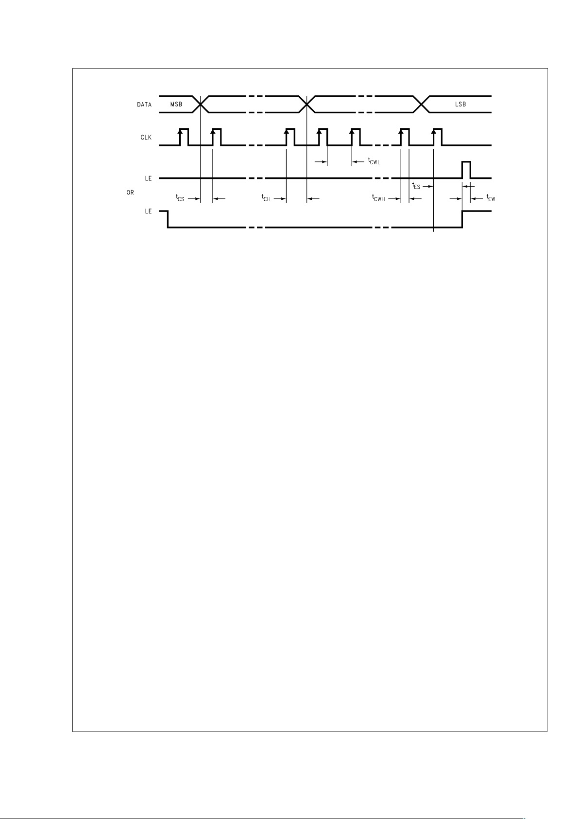
Microwire Interface Timing Diagram
20068004
LMX2502/LMX2512
www.national.com 6
Page 7

Functional Description
GENERAL DESCRIPTION
LMX2502/12 is a highly integrated frequency synthesizer
system that generates LO signals for PCS and Cellular
CDMA applications. These devices include all the functional
blocks of a PLL, RF VCO, prescaler, RF phase detector, and
loop filter. The need for external components is limited to a
few passive elements for matching the output impedance
and bypass elements for power line stabilization.
In addition to the RF circuitry, the IC also includes IF frequency dividers, and an IF phase detector to complete the IF
synthesis with the external VCO and the loop filter. Table 1
summarizes the counter values used to generate the default
IF frequencies.
Using a low spurious fractional-N synthesizer based on a
delta sigma modulator, the circuit can support 10 kHz channel spacing for PCS and Cellular CDMA systems.
The fractional-N synthesizer enables faster lock time, which
reduces power consumption and system set-up time. Additionally, the loop filter occupies a smaller area as opposed to
the integer-N architecture. This allows the loop filter to be
embedded into the circuit, minimizing the external noise
coupling and total form factor. The delta sigma architecture
delivers very low spurious, which can be a significant problem for other PLL solutions.
The circuit also supports commonly used reference frequencies of 19.20 MHz and 19.68 MHz.
FREQUENCY GENERATION
RF-PLL Section
The divide ratio can be calculated using the following equation:
LMX2502 – PCS CDMA:
f
VCO
= {8 x RF_B + RF_A + (RF_FN / f
OSC
)x104}xf
OSC
where (RF_A<RF_B)
LMX2512 – Cellular CDMA:
f
VCO
= {6 x RF_B + RF_A + (RF_FN / f
OSC
)x104}xf
OSC
where (RF_A<RF_B)
where
f
VCO
: Output frequency of voltage controlled oscillator (VCO)
RF_B: Preset divide ratio of binary 4-bit programmable
counter (2 ≤ RF_B ≤ 15)
RF_A: Preset divide ratio of binary 3-bit swallow counter (0 ≤
RF_A ≤ 7 for LMX2502 or 0 ≤ RF_A ≤ 5 for LMX2512)
RF_FN: Preset numerator of binary 11-bit modulus counter
(0 ≤ RF_FN
<
1920 for f
OSC
= 19.20 MHz or 0 ≤ RF_FN
<
1968 for f
OSC
= 19.68 MHz)
f
OSC
: Reference oscillator frequency
IF-PLL Section
f
VCO
= {16 x IF_B + IF_A} x f
OSC
/ IF_R where (IF_A<IF_B)
where
f
VCO
: Output frequency of the voltage controlled oscillator
(VCO)
IF_B: Preset divide ratio of the binary 9-bit programmable
counter (1 ≤ IF_B ≤ 511)
IF_A: Preset divide ratio of the binary 4-bit swallow counter
(0 ≤ IF_A ≤ 15)
f
OSC
: Reference oscillator frequency
IF_R: Preset divide ratio of the binary 9-bit programmable
reference counter (2 ≤ IF_R ≤ 511)
From the above equation, the LMX2502/12 generates the
fixed IF frequencies as summarized in Table 1.
TABLE 1. IF Frequencies
Device Type F
VCO
(MHz)
IF_B IF_A f
OSC
/IF_R
(kHz)
LMX2502LQ1635 440.76 229 9 120
LMX2512LQ0967 170.67 88 15 120
LMX2512LQ1065 367.20 191 4 120
VCO FREQUENCY TUNING
The center frequency of the RF VCO is determined by the
resonant frequency of the tank circuit. This tank circuit is
implemented on-chip and requires no external inductor. The
LMX2502/12 actively tunes the tank circuit to the required
frequency with the built-in tracking algorithm.
BANDWIDTH CONTROL AND FREQUENCY LOCK
During the frequency acquisition period, the loop bandwidth
is significantly extended to achieve frequency lock. Once
frequency lock occurs, the PLL will return to a steady state
condition with the loop bandwidth set to its nominal value.
The transition between acquisition and lock modes occurs
seamlessly and extremely fast, thereby, meeting the stringent requirements associated with lock time and phase
noise. Several controls (BW_DUR, BW_CRL, and BW_EN)
are used to optimize the lock time performance.
SPURIOUS REDUCTION
To improve the spurious performance of the device one of
two types of spurious reduction schemes can be selected:
•
A continuous optimization scheme, which tracks the environmental and voltage variations, giving the best spurious performance over changing conditions
•
A one time optimization scheme, which sets the internal
compensation values only when the PLL goes into a
locked state.
The spurious reduction can also be disabled, but it is recommended that the continuous optimization mode be used for
normal operation.
POWER DOWN MODE
The LMX2502 and LMX2512 include a power down mode to
reduce the power consumption. The LMX2502/12 enters into
the power down mode either by taking the CE pin LOW or by
setting the power down bits in Register R1. Table 2 summarizes the power down function. If CE is set LOW, the circuit is
powered down regardless of the register values. When CE is
HIGH, the IF and RF circuitry are individually powered down
by setting the register bits.
LMX2502/LMX2512
www.national.com7
Page 8

Functional Description (Continued)
TABLE 2. Power Down Configuration
CE Pin RF_EN IF_EN RF Circuitry IF Circuitry
0 X X OFF OFF
1 0 0 OFF OFF
1 0 1 OFF ON
1 1 0 ON OFF
111 ON ON
X = Don’t care.
LOCK DETECT
The LD output can be used to indicate the lock status of the
RF PLL. Bit 21 in Register R0 determines the signal that
appears on the LD pin. When the RF PLL is not locked, the
LD pin remains LOW. After obtaining phase lock, the LD pin
will have a logical HIGH level. The output can also be
programmed to be ground at all times.
TABLE 3. Lock Detect Modes
LD Bit Mode
0 Disable (GND)
1 Enable
TABLE 4. Lock Detect Logic
RF PLL Section LD Output
Locked HIGH
Not Locked LOW
Note 9: LD output becomes LOW when the phase error is larger than tW2.
Note 10: LD output becomes HIGH when the phase error is less than t
W1
for
four or more consecutive cycles.
Note 11: Phase Error is measured on leading edge. Only errors greater than
t
W1
and tW2are labeled.
Note 12: t
W1
and tW2are equal to 10 ns.
Note 13: The lock detect comparison occurs with every 64
th
cycle of fRand
f
N
.
20068005
FIGURE 1. Lock Detect Timing Diagram Waveform (Notes 9, 10, 11, 12, 13)
LMX2502/LMX2512
www.national.com 8
Page 9

Functional Description (Continued)
MICROWIRE INTERFACE
The programmable register set is accessed via the
MICROWIRE serial interface. The interface comprises three
signal pins: CLK, DATA, and LE (Latch Enable). Serial data
(DATA) is clocked into the 24-bit shift register on the rising
edge of the clock (CLK). The last bits decode the internal
control register address. When the latch enable (LE) transitions from LOW to HIGH, data stored in the shift registers is
loaded into the corresponding control register.
20068006
FIGURE 2. Lock Detect Flow Diagram
LMX2502/LMX2512
www.national.com9
Page 10

Programming Description
GENERAL PROGRAMMING INFORMATION
The serial interface has a 24-bit shift register to store the incoming data bits temporarily. The incoming data is loaded into the shift
register from MSB to LSB. The data is shifted at the rising edge of the clock signal. When the latch enable signal transitions from
LOW to HIGH, the data stored in the shift register is transferred to the proper register depending on the address bit settings. The
selection of the particular register is determined by the address bits equal to the binary representation of the number of the control
register.
At initial start-up, the MICROWIRE loading requires 4 default words (registers R3, loaded first, to R0, loaded last). After the device
has been initially programmed, the RF VCO frequency can be changed using a single register (R0). If an IF frequency other than
the default value for the device is desired the SPI_DEF bit should be set to 0, the desired values for IF_A, IF_B, and IF_R entered
and words R6 to R0 should be sent.
The control register content map describes how the bits within each control register are allocated to the specific control functions.
COMPLETE REGISTER MAP
Register
MSB SHIFT REGISTER BIT LOCATION LSB
23 22 21 20 19 18 17 16 15 14 13 12 11 10 9 8 7 6 5 4 3 2 1 0
R0
(Default)
SPI_
DEF
RF_
SEL
RF_LD0 RF_B
[3:0]
RF_A
[2:0]
RF_FN
[10:0]
00
R1
(Default)
IF_
FREQ
[1:0]
OSC_
FREQ
10 000000SPUR_
RDT
[1:0]
0 0 1 0 1 OB_
CRL
[1:0]
RF_ENIF_EN01
R2
(Default)
IF_
CUR[1:0]
0 01 0011101 1 01010001 0 10
R3
(Default)
BW_
DUR
[1:0]
BW_
CRL
[1:0]
BW_EN1011110 1 000110VCO_
CUR
[1:0]
011
R4 0 0 0 1 0 0 0 IF_A
[3:0]
IF_B
[8:0]
0111
R5 0 0 1 10 00010 IF_R
[8:0]
01 1 11
R6 1 0 0 00 0000000 0 00000011 1 11
NOTE: Bold numbers represent the address bits.
LMX2502/LMX2512
www.national.com 10
Page 11

Programming Description (Continued)
R0 REGISTER
The R0 register address bits (R0 [1:0]) are “00”.
The SPI_DEF bit selects between using the default IF counter values and user programmable values. The use of the default
counter values requires that only words R0 to R3 (registers R3, loaded first, to R0, loaded last) be sent after initial power up.
The RF_LD bit activates the lock detect output of the LD pin (pin 19). The lock detect mode shows the lock status of the RF PLL.
The waveform of the lock detect mode is shown in Figure 1,intheFunctional Description section on LOCK DETECT.
The RF N counter consists of the 4-bit programmable counter (RF_B counter), the 3-bit swallow counter (RF_A counter) and the
11-bit delta sigma modulator (RF_FN counter). The equations for calculating the counter values are presented below.
R0 REGISTER
Register
MSB SHIFT REGISTER BIT LOCATION LSB
23 22 21 2019181716151413121110987654321 0
Data Field Address
Field
R0
(Default)
SPI_
DEF
RF_
SEL
RF_LD0 RF_B
[3:0]
RF_A
[2:0]
RF_FN
[10:0]
00
Name Functions
SPI_DEF Default Register Selection
0 = OFF (Use values set in R0 to R6)
1 = ON (Use default values set in R0 to R3)
RF_SEL RF VCO Selection
0 = LMX2512
1 = LMX2502
RF_LD RF Lock Detect
0 = Hard zero (GND)
1 = Lock detect
RF_B [3:0] RF_B Counter
4-bit programmable counter
2 ≤ RF_B ≤ 15
RF_A [2:0] RF_A Counter
3-bit swallow counter
0 ≤ RF_A ≤ 7 for LMX2502
0 ≤ RF_A ≤ 5 for LMX2512
RF_FN [10:0] RF Fractional Numerator Counter
11-bit programmable counter
0 ≤ RF_FN
<
1920 for f
OSC
= 19.20 MHz
0 ≤ RF_FN
<
1968 for f
OSC
= 19.68 MHz
LMX2502/LMX2512
www.national.com11
Page 12

Programming Description (Continued)
RF N Counter Setting:
Counter Name Symbol Function
Modulus Counter RF_FN RF N Divider
N = Prescaler x RF_B + RF_A + (RF_FN / f
OSC
)x10
4
Programmable
Counter
RF_B
Swallow Counter RF_A
Pulse Swallow Function:
f
VCO
= {Prescaler x RF_B + RF_A + (RF_FN / f
OSC
)x104}xf
OSC
where (RF_A<RF_B)
where
f
VCO
: Output frequency of voltage controlled oscillator (VCO)
Prescaler Values:
Device Type RF Prescaler
LMX2502 8
LMX2512 6
RF_B: Preset divide ratio of binary 4-bit programmable counter (2 ≤ RF_B ≤ 15)
RF_A: Preset divide ratio of binary 3-bit swallow counter (0 ≤ RF_A ≤ 7 for LMX2502, 0 ≤ RF_A ≤ 5 for LMX2512)
RF_FN: Preset numerator of binary 11-bit modulus counter (0 ≤ RF_FN
<
1920 for f
OSC
= 19.20 MHz; 0 ≤ RF_FN<1968 for f
OSC
= 19.68 MHz).
f
OSC
: Reference oscillator frequency
NOTE: For the use of reference frequencies other than those specified, please contact National Semiconductor.
LMX2502/LMX2512
www.national.com 12
Page 13

Programming Description (Continued)
R1 REGISTER
The R1 register address bits (R1 [1:0]) are “01”.
The IF_FREQ bits selects the default IF frequency applicable to the specific CDMA system. For the LMX2502 the default IF
frequency is 440.76 MHz, and for the LMX2512 the default IF frequencies are 367.20 MHz and 170.76 MHz, depending on
variant.
Reference Frequency Selection bit (OSC_FREQ) selects either 19.20 MHz or 19.68 MHz for the reference oscillator frequency.
The internal spurious reduction scheme is controlled by the SPUR_RDT [1:0] bits. There are two different spur reduction
schemes: a continuous tracking mode and a single optimization mode. The continuous tracking mode will adjust for variations in
voltage and temperature. The single optimization mode fixes the internal compensation parameters only when the PLL goes into
the locked state. The spur reduction can also be disabled, but it is recommended that the continuous mode be used for normal
operation.
The OB_CRL [1:0] bits determine the power level of the RF output buffer. The power level can be set according to the system
requirement.
The two bits, RF_EN and IF_EN, logically select the active state of the RF synthesizer system and the IF PLL, respectively. The
entire IC can be placed in a power down state by using the CE control pin (pin 20).
R1 REGISTER
Register
MSB SHIFT REGISTER BIT LOCATION LSB
23 2221 201918171615141312 11 109876543 2 1 0
Data Field Address
Field
R1
(Default)
IF_
FREQ
[1:0]
OSC_
FREQ
10000000SPUR_
RDT
[1:0]
0 0101OB_
CRL
[1:0]
RF_ENIF_EN01
Name Functions
IF_FREQ [1:0] IF Frequency Selection
00 = 170.76 MHz (LMX2512LQ0967)
01 = 367.20 MHz (LMX2512LQ1065)
10 = 440.76 MHz (LMX2502LQ1635)
OSC_FREQ Reference Frequency Selection
0 = 19.20 MHz
1 = 19.68 MHz
SPUR_RDT [1:0] Spur Reduction Scheme
00 = No spur reduction
01 = Not Used
10 = Continuous tracking of variation (Recommended)
11 = One time optimization
OB_CRL [1:0] RF Output Power Control
00 = Minimum Output Power
01 =
10 =
11 = Maximum Output Power
RF_EN RF Enable
0=RFOff
1=RFOn
IF_EN IF Enable
0=IFOff
1=IFOn
LMX2502/LMX2512
www.national.com13
Page 14

Programming Description (Continued)
R2 REGISTER
The R2 Register address bits (R2 [1:0]) are “10”.
The IF_CUR [1:0] bits program the IF charge-pump current. Considering the external IF VCO and loop filter, the user can select
the amount of IF charge pump current to be 100 µA, 200 µA, 300 µA or 800 µA.
R2 REGISTER
Register
MSB SHIFT REGISTER BIT LOCATION LSB
23 22212019181716151413121110987654321 0
Data Field Address
Field
R2
(Default)
IF_
CUR[1:0]
0010011101101010001010
Name Functions
IF_CUR [1:0] IF Charge Pump Current
00 = 100 µA
01 = 200 µA
10 = 300 µA
11 = 800 µA
LMX2502/LMX2512
www.national.com 14
Page 15

Programming Description (Continued)
R3 REGISTER
The R3 register address bits (R3 [2:0]) are “011”.
Register R3 contains the controls for the phase lock bandwidth controls (BW_DUR, BW_CRL, and BW_EN). The duration of the
digital controller portion of the bandwidth control is set by BW_DUR [1:0]. The minimum time set with 00 and increasing durations
to the maximum value set with 11. BW_CRL [1:0] sets the phase offset criterion for the bandwidth controller. Once the phase
offset between the reference clock and the divided VCO signal are within the set criterion, the bandwidth control stops. The
maximum phase offset is set with 00 and decreases to the minimum value set with 11. BW_EN enables the bandwidth control in
the locking state.
The VCO dynamic current is also controlled in register R3 with VCO_CUR [1:0]. The minimum value corresponds to 00 and
increases to a maximum value set at 11.
R3 REGISTER
Register
MSB SHIFT REGISTER BIT LOCATION LSB
23 22212019 181716151413121110987654 3 210
Data Field Address
Field
R3
(Default)
BW_
DUR
[1:0]
BW_
CRL
[1:0]
BW_EN10111101000110VCO_
CUR
[1:0]
011
Name Functions
BW_DUR [1:0] Bandwidth Duration
00 = Minimum value (Recommended)
01 =
10 =
11 = Maximum value
BW_CRL [1:0] Bandwidth Control
00 = Maximum phase offset (Recommended)
01 =
10 =
11 = Minimum phase offset
BW_EN Bandwidth Enable
0 = Disable
1 = Enable (Recommended)
VCO_CUR [1:0] VCO Dynamic Current
00 = Minimum value
01 =
10 =
11 = Maximum value (Recommended)
LMX2502/LMX2512
www.national.com15
Page 16

Programming Description (Continued)
R4 REGISTER
The R4 register address bits (R3 [3:0]) are “0111”.
Register R4 is used to set the IF N counters if the default value is not desired. This register is only active if the SPI_DEF bit in
register R0 is 0.
R4 REGISTER
Register
MSB SHIFT REGISTER BIT LOCATION LSB
23 222120191817161514131211109876543210
Data Field Address
Field
R4 0 001000 IF_A
[3:0]
IF_B
[8:0]
0111
Name Functions
IF_A [3:0] IF A Counter
4-bit swallow counter
0 ≤ IF_A ≤ 15
IF_B [8:0] IF B Counter
9-bit programmable counter
1 ≤ IF_B ≤ 511
IF Frequency Setting:
f
VCO
= {16 x IF_B + IF_A} x f
OSC
/ IF_R where (IF_A<IF_B)
where
f
VCO
: Output frequency of IF voltage controlled oscillator (IF VCO)
IF_B: Preset divide ratio of binary 9-bit programmable counter (1 ≤ IF_B ≤ 511)
IF_A: Preset divide ratio of binary 4-bit swallow counter (0 ≤ IF_A ≤ 15)
IF_R: Preset divide ratio of binary 9-bit programmable reference counter (2 ≤ IF_R ≤ 511)
f
OSC
: Reference oscillator frequency
LMX2502/LMX2512
www.national.com 16
Page 17

Programming Description (Continued)
R5 REGISTER
The R5 register address bits (R5 [4:0]) are “01111” .
Register R5 is used to set the IF_R divider if the default value is not desired. This register is only active if the SPI_DEF bit in
register R0 is 0.
R5 REGISTER
Register
MSB SHIFT REGISTER BIT LOCATION LSB
23 222120191817161514131211109876543210
Data Field Address
Field
R5 0 011000010 IF_R
[8:0]
01111
Name Functions
IF_R [8:0] IF R Counter
9-bit programmable counter
2 ≤ IF_R ≤ 511
R6 REGISTER
The R6 register address bits (R6 [5:0]) are “011111” .
Register R6 is used for internal testing of the device and is not intended for customer use. This register is only active if the
SPI_DEF bit in register R0 is 0.
R6 REGISTER
Register
MSB SHIFT REGISTER BIT LOCATION LSB
23 222120191817161514131211109876543210
Data Field Address Field
R6 1 00000000000000000011111
LMX2502/LMX2512
www.national.com17
Page 18

Physical Dimensions inches (millimeters) unless otherwise noted
Leadless Leadframe Package (LLP)
NS Package Number LQA28A
LIFE SUPPORT POLICY
NATIONAL’S PRODUCTS ARE NOT AUTHORIZED FOR USE AS CRITICAL COMPONENTS IN LIFE SUPPORT
DEVICES OR SYSTEMS WITHOUT THE EXPRESS WRITTEN APPROVAL OF THE PRESIDENT AND GENERAL
COUNSEL OF NATIONAL SEMICONDUCTOR CORPORATION. As used herein:
1. Life support devices or systems are devices or
systems which, (a) are intended for surgical implant
into the body, or (b) support or sustain life, and
whose failure to perform when properly used in
accordance with instructions for use provided in the
labeling, can be reasonably expected to result in a
significant injury to the user.
2. A critical component is any component of a life
support device or system whose failure to perform
can be reasonably expected to cause the failure of
the life support device or system, or to affect its
safety or effectiveness.
National Semiconductor
Americas Customer
Support Center
Email: new.feedback@nsc.com
Tel: 1-800-272-9959
National Semiconductor
Europe Customer Support Center
Fax: +49 (0) 180-530 85 86
Email: europe.support@nsc.com
Deutsch Tel: +49 (0) 69 9508 6208
English Tel: +44 (0) 870 24 0 2171
Français Tel: +33 (0) 1 41 91 8790
National Semiconductor
Asia Pacific Customer
Support Center
Email: ap.support@nsc.com
National Semiconductor
Japan Customer Support Center
Fax: 81-3-5639-7507
Email: jpn.feedback@nsc.com
Tel: 81-3-5639-7560
www.national.com
LMX2502/LMX2512 Frequency Synthesizer System with Integrated VCO
National does not assume any responsibility for use of any circuitry described, no circuit patent licenses are implied and National reserves the right at any time without notice to change said circuitry and specifications.
 Loading...