

Page 1
LMX2370/LMX2371/LMX2372
PLLatinum
™
Dual Frequency Synthesizer for RF
Personal Communications
LMX2370 2.5 GHz/1.2 GHz
LMX2371 2.0 GHz/1.2 GHz
LMX2372 1.2 GHz/1.2 GHz
General Description
The LMX237X family of monolithic, integrated dual frequency synthesizers, including prescalers, is designed to be
used as a first and second local oscillator for dual mode or
dual conversion transceivers. It is fabricated using National’s
0.5u ABiCV silicon BiCMOS process. The LMX237X contains two dual modulus prescalers. A 32/33 or a 16/17
prescaler can be selected for the 2.5 GHz and 2.0 GHz RF
synthesizers with the 16/17 prescaler rated for input frequencies below 1.2 GHz. A 16/17 or an 8/9 prescaler can be selected for the 1.2 GHz RF synthesizers with the 8/9 prescaler
rated for input frequencies below 550 MHz. Using a digital
phase locked loop technique, the LMX237X can generate
very stable, low noise control signals for UHF and VHF voltage controlled oscillators (VCO’s). Serial data is transferred
into the LMX237X via a 1.8V three wire interface (Data, Enable, Clock) compatible with low voltage baseband processors. Supply voltage can range from 2.7V to 5.5V. The
LMX237X family features very low current consumption typically: LMX2370 - 6.0 mA
@
3V, LMX2371 - 5.0 mA@3V,
LMX2372 - 4.0 mA
@
3V.
The LMX237X are available in a 24-pad chip scale (CSP) or
a 20-pin TSSOP surface mount plastic package.
Features
n 2.7V–5.5V operation
n Ultra low current consumption
n Low phase detector noise floor
n Low voltage MICROWIRE
™
interface (1.8V up to VCC)
n Low prescaler values
32/33
@
fIN≤ 2.5 GHz
16/17
@
fIN≤ 1.2 GHz
8/9
@
fIN≤ 550 MHz
n Selectable charge pump current levels
n Selectable FastLock
™
mode
n Enhanced ESD protection
n Small 24 pad chip scale package (3.5 x 4.5 x 1.0 mm)
Applications
n Portable wireless communications (PCS/PCN, cordless)
n Dual mode cellular telephone systems
n Spread spectrum communication systems (CDMA)
n Cable TV tuners (CATV)
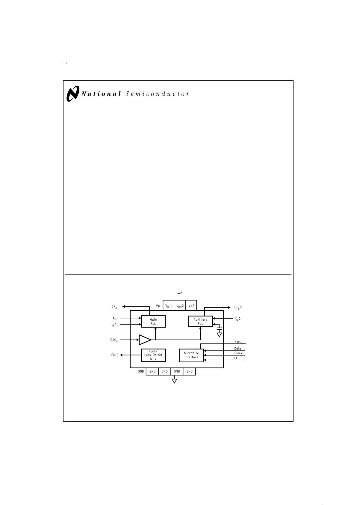
Functional Block Diagram
FastLock™, PLLatinum™and MICROWIRE™are trademarks of National Semiconductor Corporation.
TRI-STATE
®
is a registered trademark of National Semiconductor Corporation.
DS101026-1
PRELIMINARY
March 1999
LMX2370/LMX2371/LMX2372 PLLatinum Dual Frequency Synthesizer for RF Personal
Communications
© 1999 National Semiconductor Corporation DS101026 www.national.com
Page 2
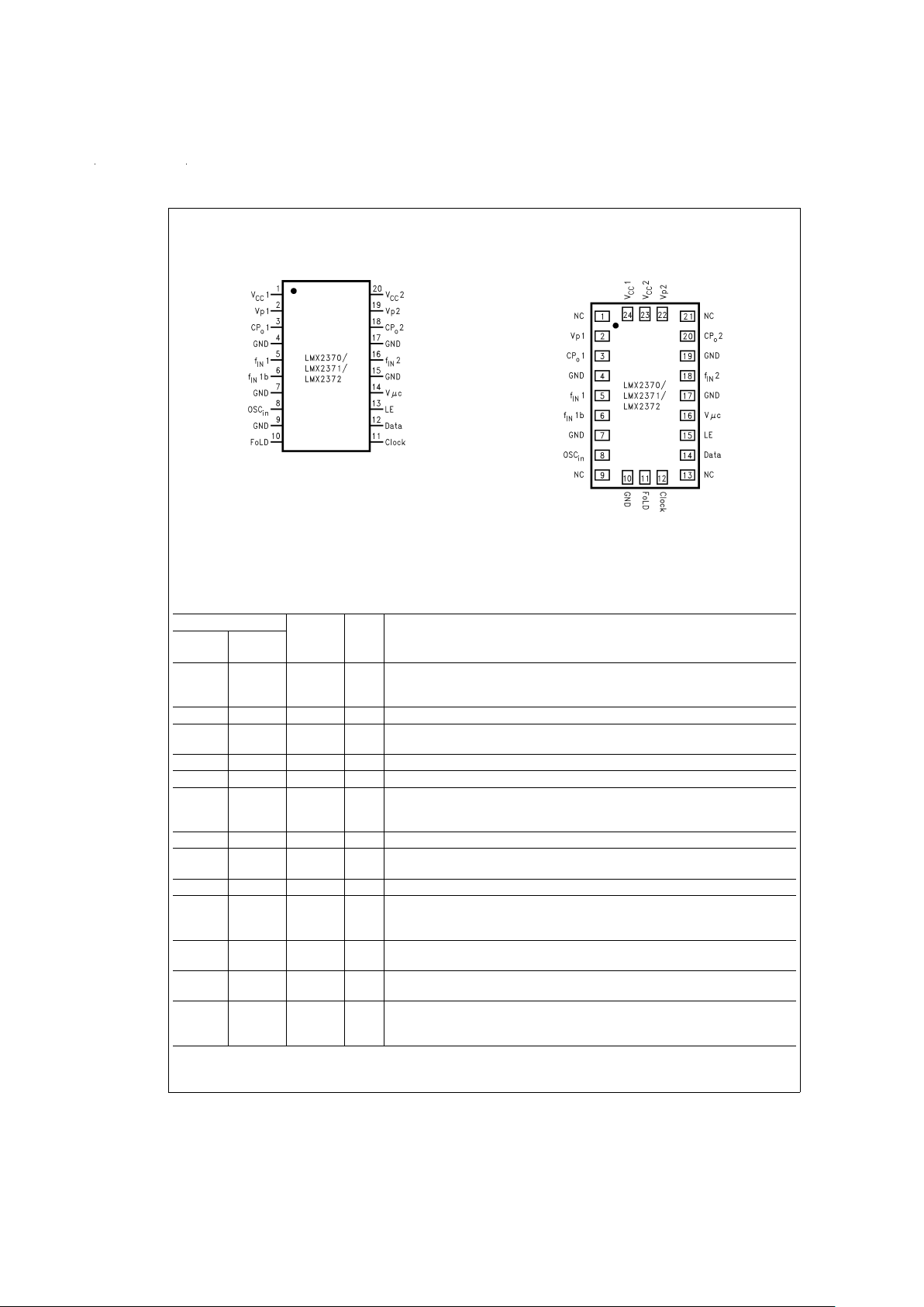
Connection Diagrams
Pin Descriptions
Pin No.
Pin
Name
I/O Description
24-Pin
CSP
20-Pin
TSSOP
24 1 V
CC
1 — Power supply voltage input for RF analog and RF digital circuits. Input may range
from 2.7V to 5.5V. V
CC
1 must equal VCC2. Bypass capacitors should be placed as
close as possible to this pin and be connected directly to the ground plane.
2 2 Vp1 — Power supply for Main charge pump. Must be ≥ V
CC
.
33CP
o
1 O Internal Main charge pump output. For connection to a loop filter for driving the
input of an external VCO.
4 4 GND — Ground for Main digital circuitry.
55f
IN
1 I Main prescaler input. Small signal input from the VCO.
66f
IN
1b I Main prescaler complementary input. For single ended operation, a bypass
capacitor should be placed as close as possible to this pin and be connected
directly to the ground plane.
7 7 GND — Ground for Main analog circuitry.
8 8 OSC
in
I Oscillator input. The input has a VCC/2 input threshold and can be driven from an
external CMOS or TTL logic gate.
10 9 GND — Ground for Aux digital, MICROWIRE, FoLD, and oscillator circuits.
11 10 Fo/LD O Multiplexed output of the Main/Aux programmable or reference dividers,
Main/Auxiliary lock detect signals and Fastlock mode. CMOS output
(see
Programmable Modes in the Datasheet).
12 11 Clock I High impedance CMOS Clock input. Data for the various counters is clocked in on
the rising edge, into the 22-bit shift register.
14 12 Data I Binary serial data input. Data entered MSB first. The last two bits are the control
bits. High impedance CMOS input.
15 13 LE I Load enable. High impedance CMOS input. When LE goes HIGH, data stored in
the shift registers is loaded into one of the 4 appropriate latches (control bit
dependent).
TSSOP 20-Pin Package
DS101026-2
Top View
Order Number LMX2370TM, LMX2370TMX,
LMX2371TM, LMX2371TMX,
LMX2372TM or LMX2372TMX
See NS Package Number MTC20
CSP 24-Pin Package
DS101026-3
Top View
Order Number LMX2370SLBX,
LMX2371SLBX or LMX2372SLBX
See NS Package Number SLB24A
www.national.com 2
Page 3
Pin Descriptions (Continued)
Pin No.
Pin
Name
I/O Description
24-Pin
CSP
20-Pin
TSSOP
16 14 Vµc — Power supply for MICROWIRE circuitry. Must be ≤ V
CC
. Typically connected to
same supply level as µprocessor or baseband controller to enable programming at
low voltages.
17 15 GND — Ground for Aux analog circuitry.
18 16 f
IN
2 I Auxiliary prescaler input. Small signal input from the VCO.
19 17 GND — Ground for Aux digital, MICROWIRE, FoLD, and oscillator.
20 18 CP
o
2 O Aux internal charge pump output. For connection to a loop filter for driving the
input of an external VCO.
22 19 Vp2 — Power supply for Aux charge pump. Must be ≥ V
CC
.
23 20 V
CC
2 — Power supply voltage input for Aux analog, Aux digital, FoLD, and oscillator
circuits. Input may range from 2.7V to 5.5V. V
CC
2 must equal VCC1. Bypass
capacitors should be placed as close as possible to this pin and be connected
directly to the ground plane.
1, 9,
13, 21
— NC — No Connect
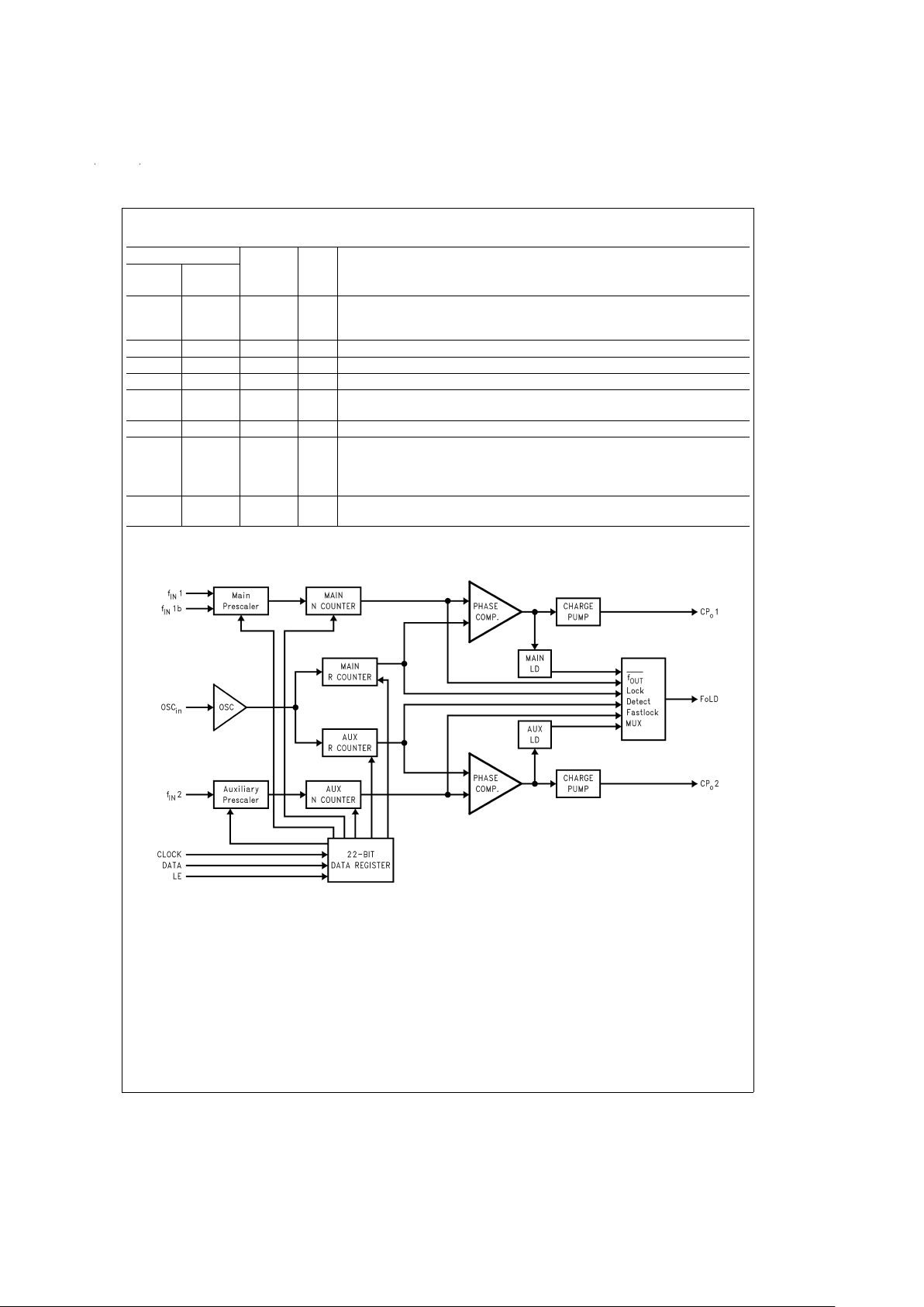
Block Diagram
DS101026-4
www.national.com3
Page 4
Absolute Maximum Ratings (Notes 1, 2)
If Military/Aerospace specified devices are required,
please contact the National Semiconductor Sales Office/
Distributors for availability and specifications.
Power Supply Voltage
V
CC
1 −0.3V to 6.5V
V
CC
2 −0.3V to 6.5V
Vp1 −0.3V to 6.5V
Vp2 −0.3V to 6.5V
Vµc −0.3V to 6.5V
Voltage on any pin with
GND=0V (V
I
) −0.3V to VCC+0.3V
Storage Temperature Range (T
S
) −65˚C to +150˚C
Lead Temperature (solder, 4 sec.) (T
L
) +260˚C
ESD - Human Body Model (Note 2) TBD
Recommended Operating
Conditions
(Note 3)
Power Supply Voltage
V
CC
1 2.7V to 5.5V
V
CC
2 2.7V to 5.5V
V
CC
1–VCC2 −0.2V to 0.2V
Vp1 V
CC
to 5.5V
Vp2 V
CC
to 5.5V
Vµc 1.72V to V
CC
Operating Temperature (TA) −40˚C to +85˚C
Note 1: Absolute Maximum Ratings indicate limits beyond which damage to
the device may occur.Operating Ratings indicate conditions for which the device is intended to be functional, but do not guarantee specific performance
limits. For guaranteed specifications and test conditions, see the Electrical
Characteristics. The guaranteed specifications apply only for the test conditions listed.
Note 2: This device is a high performance RF integrated circuit and is ESD
sensitive. Handling and assembly of this device should only be done at ESD
free workstations.
Note 3: V
CC
is defined as V
CC
=
V
CC
1=VCC2.
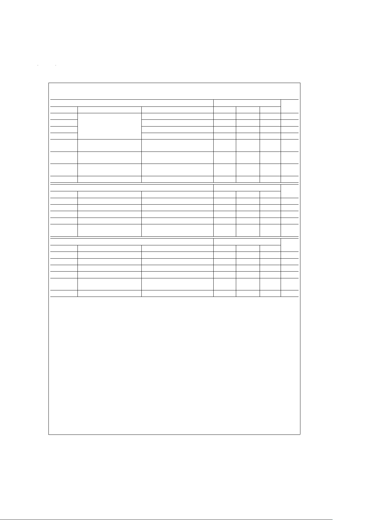
Electrical Characteristics (V
CC
=Vp=
Vµc=3.0V; −40˚C
<
T
A
<
85˚C except as specified).
GENERAL Value
Unit
Symbol Parameter Conditions Min Typ Max
I
CC
Power Supply
Current
LMX2370 Main=On, Aux=On 6 8.5 mA
LMX2371 Main=On, Aux=On 5 7.5 mA
LMX2372 Main=On, Aux=On 4 6.0 mA
LMX2370
/71/72
Aux Only
2 3.25 mA
I
CC-PWDN
Power Down Current EN_Main, EN_Aux=01550µA
f
IN
1 Main PLL
Operating
Frequency
LMX2370 P=32/33 1.2 2.5 GHz
P = 16/17 45 1200 MHz
LMX2371 P = 32/33 1.2 2.0 GHz
P = 16/17 45 1200 MHz
LMX2372 P = 16/17 45 1200 MHz
P = 8/9 45 550 MHz
f
IN
2 Auxiliary PLL Operating
Frequency
P = 16/17 45 1200 MHz
P = 8/9 45 550 MHz
Zf
IN
Main Main PLL Input Impedance RF On, f
IN
=
1800 MHz TBD Ω
RF Off, f
IN
=
1800 MHz TBD Ω
Zf
IN
Aux Aux Input Impedance f
IN
=
120 MHz TBD Ω
fφ Phase Detector Frequency 10 MHz
Pf
IN
1, PfIN2 RF Input Sensitivity 2.7 ≤ VCC≤ 3.6V −15 0 dBm
3.6 ≤ V
CC
≤ 5.5V −10 0 dBm
OSCILLATOR INPUT Value
Unit
Symbol Parameter Conditions Min Typ Max
OSC
in
Reference Oscillator Input
Operating Frequency
2 50 MHz
Z
IN
OSC OSC Input Impedance OSC On, Freq = 10 MHz TBD kΩ
OSC Off, Freq = 10 MHz TBD kΩ
V
OSC
Oscillator Input Sensitivity OSC
in
0.5 V
CC
V
PP
I
IH
OSCinInput Current VIH=VCC= 5.5V 100 µA
I
IL
OSCinInput Current VIL=0,VCC= 5.5V −100 µA
www.national.com 4
Page 5
Electrical Characteristics (V
CC
=Vp=
Vµc=3.0V; −40˚C
<
T
A
<
85˚C except as specified). (Continued)
CHARGE PUMP Value
Unit
Symbol Parameter Conditions Min Typ Max
ICP
o-source
Main and Auxiliary Charge
Pump Output Current (Note 4)
VCP
o
=
Vp/2, ICP
o
_4X=0 1.0 mA
ICP
o-sink
VCP
o
=
Vp/2, ICP
o
_4X=0 −1.0 mA
ICP
o-source
VCP
o
=
Vp/2, ICP
o
_4X=1 4.0 mA
ICP
o-sink
VCP
o
=
Vp/2, ICP
o
_4X=1 −4.0 mA
ICP
o-TRI
Charge Pump TRI-STATE
®
Current
0.5 ≤ VCP
o
≤ Vp − 0.5,
−40˚C
<
T
A
<
85˚C
−2.5 0.1 2.5 nA
ICP
o-sink
vs
ICP
o-source
CP Sink vs Source Mismatch VCP
o
=
Vp/2, T
A
=
25˚C
310
%
ICP
o
vs
VCP
o
CP Current vs Voltage 0.5 ≤ VCPo≤ Vp − 0.5, T
A
=
25˚C
815
%
ICP
o
vs TACP Current vs Temperature VCP
o
=
Vp/2, −40˚C
<
T
A
<
85˚C 8
%
DIGITAL INTERFACE (DATA, CLOCK, LE) Value
Unit
Symbol Parameter Conditions Min Typ Max
V
IH
High-Level Input Voltage Vµc=1.72V to 5.5V 0.8 Vµc V
V
IL
Low-Level Input Voltage Vµc=1.72V to 5.5V 0.2 Vµc V
I
IH
High-Level Input Current V
IH
=
Vµc=5.5V −1.0 1.0 µA
I
IL
Low-Level Input Current V
IL
=
0, Vµc=5.5V −1.0 1.0 µA
V
OL
Low-Level Output Current I
OL
=
1.0 mA, V
EXT
=
1.8V (Note
5)
0.1 0.4 V
MICROWIRE TIMING Value
Unit
Symbol Parameter Conditions Min Typ Max
t
CS
Data to Clock Setup Time See Data Input Timing 50 ns
t
CH
Data to Clock Hold Time See Data Input Timing 20 ns
t
CWH
Clock Pulse Width High See Data Input Timing 50 ns
t
CWL
Clock Pulse Width Low See Data Input Timing 50 ns
t
ES
Clock to Load Enable Setup
Time
See Data Input Timing
50 ns
t
EW
Load Enable Pulse Width See Data Input Timing 50 ns
Note 4: Main and Auxiliary Charge Pump magnitude are controlled by Main_ICPo_4X and Aux_ICPo_4X bits respectively.
Note 5: Lock Detect open drain output only pulled up to V
EXT
. Typically V
EXT
=
V
CC
.
1.0 Functional Description
The basic phase-lock-loop (PLL) configuration consists of a high-stability crystal reference oscillator, a frequency synthesizer
such as the National Semiconductor LMX2370/2371/2372, a voltage controlled oscillator (VCO), and a passive loop filter.The frequency synthesizer includes a phase detector, a current mode charge pump, as well as programmable reference [R] and feedback [N] frequency dividers. The VCO frequency is established by dividing the crystal reference signal down via the R-counter to
obtain a comparison reference frequency. This reference signal (
f
R
) is then presented to the input of a phase/frequency detector
and compared with the feedback signal (
f
N
), which is obtained by dividing the VCO frequency down by way of the N-counter.The
phase/frequency detector’s current source output pumps charge into the loop filter, which then integrates into the VCO’s control
voltage. The function of the phase/frequency comparator is to adjust the control voltage presented to the VCO until the feedback
signal frequency and phase match that of the reference signal. When this “Phase-Locked” condition exists, the VCO frequency
will be N times that of the comparison frequency, where N is the integer divide ratio.
1.1 REFERENCE OSCILLATOR INPUT
The reference oscillator frequency for the Main and Auxiliary PLLs is provided from the external reference through the OSC
in
pin.
OSC
in
can operate up to 50 MHz with input sensitivity of 0.5 VPP. The OSCinpin drives both the Main R-counter and the Auxiliary
R-counter.The input has a V
CC
/2 input threshold that can be driven from an external CMOS or TTL logic gate. Typically,the OSC
in
is connected to the output of a crystal oscillator.
1.2 REFERENCE DIVIDERS (R-COUNTERS)
The Main and Auxiliary R-counters are both clocked through the oscillator block in common. The maximum frequency is 50 MHz.
Both R-counters are CMOS design and 15-bit in length with programmable divider ratio from 2 to 32,767.
www.national.com5
Page 6

1.0 Functional Description (Continued)
1.3 PRESCALERS
The complimentary f
IN
and f
INB
inputs drive a differential-pair amplifier which feeds to the respective prescaler. The Main PLL
complementary f
IN
1 and fIN1b inputs can be driven differentially, or the negative input can be AC coupled to ground through an
external capacitor for single ended configuration. The Auxiliary PLL has the complimentary input AC coupled to ground through
an internal 10 pF capacitor. The Auxilllary PLL complimentary input is not brought out to a pin, and is intended for single ended
configuration only. The LMX237X has a dual modulus prescaler with 2 selectable modulo. For PLL’s rated at 2.5 GHz or 2.0 GHz
a 32/33 or 16/17 prescaler is available. For PLL’s rated at 1.2 GHz a 16/17 or 8/9 can be chosen. Both Main and Auxiliary prescalers’ outputs drive the subsequent CMOS flip-flop chain comprising the programmable N feedback counters. The proper prescaler value must be chosen to in order not to exceed the maximum CMOS frequency.For f
IN
>
1.2 GHz, the 32/33 prescaler must
be selected, similarly for f
IN
>
550 MHz, the prescaler value must be at least 16/17, and for f
IN
<
550 MHz, an 8/9 prescaler value
is allowable.
1.4 FEEDBACK DIVIDERS (N-COUNTERS)
The Main andAuxiliary N-counters are clocked by the output of Main and Aux prescalers respectively.The N-counter is composed
of a 13-bit integer divider and a 5-bit swallow counter. Selecting a 32/33 prescaler provides a minimum continuous divider range
from 992 to 262,143 while selecting a 16/17 or 8/9 prescaler value allows for continuous divider values between and 240 to
131,087 and 56 to 65,559 respectively.
1.5 PHASE/FREQUENCY DETECTORS
The phase/frequency detectors are driven from their respective N- and R-counter outputs. The maximum frequency at the phase
detector inputs is 10 MHz unless limited by the minimum continuous divide ratio of the dual-modulus prescaler. The phase detector output controls the charge pump. The polarity of the pump-up or pump-down control is programmed using Main_PD_POL
or Aux_PD_POL, depending on whether Main or Auxiliary VCO characteristics is positive or negative. The phase detector also
receives a feedback signal from the charge pump in order to eliminate dead zone.
1.6 CHARGE PUMPS
The phase detector’s current source output pumps charge into an external loop filter, which then integrates into the VCO’s control
voltage. The charge pump steers the charge pump output CP
o
to VP(pump-up) or Ground (pump-down). When locked, CPois
primarily in a TRI-STATE mode with small corrections. The charge pump output current magnitude can be selected as 1.0 mA or
4.0 mA by programming the Main_ICP
o
_4X or Aux_ICPo_4X bits.
1.7 MICROWIRE SERIAL INTERFACE
The programmable register set is accessed through the Microwire serial interface. The interface is comprised of three signal pins:
clock, data and load enable (LE). The supply for the MICROWIRE circuitry is separate from the rest of the IC to allow for controller
voltages down to 1.8V.Serial data is clocked into the 22-bit shift register upon the rising edge of clock. The MSB bit of data shifts
first. The last two bits decode the internal register address. On the rising edge of LE, data stored in the shift register is loaded into
one of the four latches according to the address bits. The synthesizer can be programmed even in power down state. A complete
programming description is followed in Section 2.0.
1.8 MULTIFUNCTION OUTPUTS
The LMX2370/LMX2371/LMX2372 FoLD output pin can be configured as the FastLock output or CMOS programmed output,
analog lock detects as well as showing the internal block status such as the counter outputs.
1.8.1 Lock Detect Output
An analog lock detect status generated from the phase detector is available on the Fo/LD output pin, if selected. The lock detect
output goes high when the charge pump is inactive. It goes low when the charge pump is active during a comparison cycle. The
lock detect signal output is an open drain configuration. When a PLL is in power down mode, the respective lock detect output
is always high.
1.8.2 FastLock Outputs
When configured as FastLock mode, the current can be increased 4x while maintaining loop stability by synchronously switching
a parallel loop filter resistor to ground, resulting in a
z
2x change in loop bandwidth. The zero gain crossover point of the open
loop gain, or the loop bandwidth is effectively shifted up in frequency by a factor of
√
4 = 2 during FastLock mode. For ω’=2ω,
the phase margin during FastLock will also remain constant. The charge pump current is programmed via MICROWIRE interface.
When the charge pump circuit receives an input to deliver 4 times the normal current per unit phase error, an open drain NMOS
on chip device (FoLD) switches in a second resistor element to ground. The user calculates the loop filter component values for
the normal steady state considerations. The device configuration ensures that as long as a second resistor equal to the primary
resistor value is wired in appropriately, the loop will lock faster without any additional stability considerations to account for.
1.9 POWER CONTROL
Each PLL is individually power controlled by device power-down (PWDN) bits. The Main_PWDN and Aux_PWDN bits determine
the state of power control. Activation of any PLL power-down condition results in the disabling of the respective N-counter and
de-biasing of its respective f
IN
input (to a high impedance state). The R-counter functionality also becomes disabled under this
condition.
www.national.com 6
Page 7

1.0 Functional Description (Continued)
The reference oscillator input block is powered down when both Main_PWDN and Aux_PWDN bits are asserted. The OSC
in
pin
reverts to a high impedance state when this condition exists. Power down forces the respective charge pump and phase comparator logic to a TRI-STATE condition. During the power down condition, both N- and R-counters are held at reset. Upon powering up, the N-counter resumes counting in “close” alignment with the R-counter. The maximum error is at most one prescaler
cycle. The MICROWIRE interface remains active and it is capable of loading and latching in data during all of the power down
modes.
2.0 Programming Description
2.1 MICROWIRE INTERFACE
The LMX237X register set can be accessed through the MICROWIRE interface. A22-bit shift register is used as a temporary register to indirectly program the on-chip registers. The shift register consists of a 20-bit DATA[19:0]field and a 2-bit ADDRESS[1:0]
field as shown below. The address field is used to decode the internal register address. Data is clocked into the shift register in
the direction from MSB to LSB, when the CLOCK signal goes high. On the rising edge of Load Enable (LE) signal, data stored
in the shift register is loaded into the addressed latch.
MSB LSB
DATA[19:0] ADDRESS[1:0]
21 2 1 0
2.1.1 Registers’ Address Map
When Load Enable (LE) is transitioned high, data is transferred from the 22-bit shift register into the appropriate latch depending
on the state of the ADDRESS[1:0] bits. A multiplexing circuit decodes these address bits and writes the data field to the corresponding internal register.
ADDRESS[1:0] REGISTER
FIELD ADDRESSED
0 0 Aux_R Register
0 1 Aux_N Register
1 0 Main_R Register
1 1 Main_N Register
www.national.com7
Page 8

2.0 Programming Description (Continued)
2.1.2 Registers’ Truth Table
Most Significant Bit SHIFT REGISTER BIT LOCATION Least Significant Bit
21201918171615141312111098765432 1 0
Data Field Address Field
Aux_R FoLD 1 FoLD 0 Aux_
CP
o
_
TRI
Aux_
CP
o
_
4X
Aux_
PD_
POL
Aux_R_CNTR[14:0]
00
Aux_
R19
Aux_
R18
Aux_
R17
Aux_
R16
Aux_
R15
Aux_
R14
Aux_
R13
Aux_
R12
Aux_
R11
Aux_
R10
Aux_
R9
Aux_
R8
Aux_
R7
Aux_
R6
Aux_
R5
Aux_
R4
Aux_
R3
Aux_
R2
Aux_
R1
Aux_
R0
Aux_N Aux_
PWDN
P_
Aux
Aux_B_CNTR[12:0] Aux_A_CNTR[4:0]
01
Aux_
N19
Aux_
N18
Aux_
N17
Aux_
N16
Aux_
N15
Aux_
N14
Aux_
N13
Aux_
N12
Aux_
N11
Aux_
N10
Aux_
N9
Aux_
N8
Aux_
N7
Aux_
N6
Aux_
N5
Aux_
N4
Aux_
N3
Aux_
N2
Aux_
N1
Aux_
N0
Main_R FoLD 3 FoLD 2 Main_
CP
o
_
TRI
Main_
CP
o
_
4X
Main_
PD_
POL
Main_R_CNTR[14:0]
10
Main_
R19
Main_
R18
Main_
R17
Main_
R16
Main_
R15
Main_
R14
Main_
R13
Main_
R12
Main_
R11
Main_
R10
Main_
R9
Main_
R8
Main_
R7
Main_
R6
Main_
R5
Main_
R4
Main_
R3
Main_
R2
Main_
R1
Main_
R0
Main_N Main_
PWDN
P_
Main
Main_B_CNTR[12:0] Main_A_CNTR[4:0]
11
Main_
N19
Main_
N18
Main_
N17
Main_
N16
Main_
N15
Main_
N14
Main_
N13
Main_
N12
Main_
N11
Main_
N10
Main_
N9
Main_
N8
Main_
N7
Main_
N6
Main_
N5
Main_
N4
Main_
N3
Main_
N2
Main_
N1
Main_
N0
www.national.com 8
Page 9

2.0 Programming Description (Continued)
2.2 PROGRAMMABLE REFERENCE DIVIDERS (Main and Aux R Counters)
2.2.1 Aux_R Register
If the ADDRESS[1:0] field is set to 0 0, data is transferred from the 22-bit shift register into the Aux_R register when Load Enable
(LE) signal goes high. The Aux_R register sets the Aux PLL’s 15-bit R-counter divide ratio and various programmable modes. The
divide ratio is put into the Aux_R_CNTR[14:0] field. The divider ratio must be ≥ 2. For the description of bits Aux_R15–Aux_R19
see Section 2.4.
Most Significant Bit SHIFT REGISTER BIT LOCATION Least Significant Bit
21201918171615141312111098765432 1 0
Data Field Address Field
Aux_R
FoLD 1
FoLD 0
Aux_CP
o
_TRI
Aux_CP
o
_4X
Aux_PD_POL
Aux_R_CNTR[14:0]
00
Aux_R19
Aux_R18
Aux_R17
Aux_R16
Aux_R15
Aux_R14
Aux_R13
Aux_R12
Aux_R11
Aux_R10
Aux_R9
Aux_R8
Aux_R7
Aux_R6
Aux_R5
Aux_R4
Aux_R3
Aux_R2
Aux_R1
Aux_R0
2.2.2 Main_R Register
If the ADDRESS[1:0] field is set to 1 0, data is transferred from the 22-bit shift register into the Main_R register which sets the
Main PLL’s 15-bit R-counter divide ratio when Load Enable (LE) signal goes high. The divide ratio is put into the
Main_R_CNTR[14:0] field. The divider ratio must be ≥ 2. For the description of bits Main_R15–Main_R19 see Section 2.4.
Most Significant Bit SHIFT REGISTER BIT LOCATION Least Significant Bit
21201918171615141312111098765432 1 0
Data Field Address Field
Main_R
FoLD 3
FoLD 2
Main_CP
o
_TRI
Main_CP
o
_4X
Main_PD_POL
Main_R_CNTR[14:0]
10
Main_R19
Main_R18
Main_R17
Main_R16
Main_R15
Main_R14
Main_R13
Main_R12
Main_R11
Main_R10
Main_R9
Main_R8
Main_R7
Main_R6
Main_R5
Main_R4
Main_R3
Main_R2
Main_R1
Main_R0
2.2.3 Reference Divide Ratio (Main and Auxiliary R-Counters)
If the ADDRESS[1:0] field is set to00or10(00forAuxand10forMain) data is transferred MSB first from the 22-bit shift register
into a latch which sets the respective 15-bit R-counter. Serial data format is shown below.
Main_R_CNTR[14:0] or Aux_R_CNTR[14:0]
Divide Ratio R14 R13 R12 R11 R10 R9 R8 R7 R6 R5 R4 R3 R2 R1 R0
2 000000000000010
3 000000000000011
• •••••••••••••••
32,767 111111111111111
Note: R-counter divide ratio must be from 2 to 32,767.
2.3 PROGRAMMABLE FEEDBACK [N] DIVIDERS
2.3.1 Aux_N Register
If the ADDRESS[1:0] field is set to 0 1, data is transferred from the 22-bit shift register into the Aux_N register which sets the Auxiliary PLL’s 18-bit N-counter, prescaler value and power-down bit. The 18-bit N-counter consists of a 5-bit swallow
counter, Aux_A_CNTR[4:0], and a 13-bit programmable counter, Aux_B_CNTR[12:0]. Serial data format is shown below.
www.national.com9
Page 10

2.0 Programming Description (Continued)
Most Significant Bit SHIFT REGISTER BIT LOCATION Least Significant Bit
21201918171615141312111098765432 1 0
Data Field Address Field
Aux_N
Aux_PWDN
P_Aux
Aux_B_CNTR[12:0] Aux_A_CNTR[4:0]
01
Aux_N19
Aux_N18
Aux_N17
Aux_N16
Aux_N15
Aux_N14
Aux_N13
Aux_N12
Aux_N11
Aux_N10
Aux_N9
Aux_N8
Aux_N7
Aux_N6
Aux_N5
Aux_N4
Aux_N3
Aux_N2
Aux_N1
Aux_N0
2.3.2 Main_N Register
If the ADDRESS[1:0] field is set to 1 1, data is transferred from the 22-bit shift register into the Main_N register which sets the
Main PLL’s 18-bit N-counter, prescaler value and power-down bit. The 18-bit N-counter consists of a 5-bit swallow counter,
Main_A_CNTR[4:0], and a 13-bit programmable counter, Main_B_CNTR[12:0]. Serial data format is shown below.
Most Significant Bit SHIFT REGISTER BIT LOCATION Least Significant Bit
21201918171615141312111098765432 1 0
Data Field
Address Field
Main_N
Main_PWDN
P_Main
Main_B_CNTR[12:0] Main_A_CNTR[4:0]
11
Main_N19
Main_N18
Main_N17
Main_N16
Main_N15
Main_N14
Main_N13
Main_N12
Main_N11
Main_N10
Main_N9
Main_N8
Main_N7
Main_N6
Main_N5
Main_N4
Main_N3
Main_N2
Main_N1
Main_N0
2.3.3 Feedback Divide Ratio (Main B Counter, Auxiliary B Counter)
Main_B_CNTR[12:0] or Aux_B_CNTR[12:0]
Divide Ratio N17 N16 N15 N14 N13 N12 N11 N10 N9 N8 N7 N6 N5
3 0000000000011
4 0000000000101
• •••••••••••••
8,191 1111111111111
Note: B-counter divide ratio must be ≥ 3.
2.3.4 Swallow Counter Divide Ratio (Main A Counter, Auxiliary A Counter)
Main_A_CNTR[4:0] or Aux_A_CNTR[4:0]
Divide Ratio Main_N4 Main_N3 Main_N2 Main_N1 Main_N0
0 00000
1 00001
• •••••
31 11111
Notes: A<P, B>A.
www.national.com 10
Page 11

2.0 Programming Description (Continued)
2.3.5 PLL Prescaler Select (P_Aux, P_Main)
The LMX2370, LMX2371 and LMX2372 contain two dual modulus prescalers. A 32/33 or a 16/17 prescaler can be selected for
the 2.5 GHz and 2.0 GHz RF synthesizers in the LMX2370 and LMX2371 respectively.The 16/17 prescaler is only rated for input
frequencies below 1.2 GHz. A 16/17 or an 8/9 prescaler can be selected for the both 1.2 GHz synthesizers on the LMX2372 as
well as the 1.2 GHz synthesizers on the LMX2370 and LMX2371. The 8/9 prescaler is only rated for input frequencies below
550 MHz.
Prescaler Value
P_Main, (Main_N18) or
P_Aux (Aux_N18)
2.5 GHz PLL 2.0 GHz PLL 1.2 GHz PLL
0 16/17 16/17 8/9
1 32/33 32/33 16/17
Allowable Prescaler Values
PLL Input Frequency 2.5 GHz PLL 2.0 GHz PLL 1.2 GHz PLL
f
IN
>
1.2 GHz 32/33 32/33 NA
550
<
f
IN
<
1200 MHz 16/17 or 32/33 16/17 or 32/33 16/17
f
IN
<
550 MHz 16/17 or 32/33 16/17 or 32/33 8/9 or 16/17
2.3.5.1 Pulse Swallow Function
f
VCO
=
[(PxB)+A]xf
OSC
/R
f
VCO
: Output frequency of external voltage controlled oscillator (VCO)
B: Preset divide ratio of binary 13-bit programmable counter (3 to 8191)
A: Preset divide ratio of binary 5-bit swallow counter
0 ≤ A ≤ 31 {P=32}
0 ≤ A ≤ 15 {P=16}
0 ≤ A ≤ 7{P=8}
A ≤ B
f
OSC
: Output frequency of the external reference frequency oscillator
R: Preset divide ratio of binary 15-bit programmable reference counter (3 to 32767)
P: Preset modulus of dual modulus prescaler (P=8, 16, or 32)
2.3.6 PLL Power Down Control (Aux_PWDN, Main_PWDN)
The Aux_PWDN (Aux_N19) and Main_PWDN (Main_N19) bits are used to power down either the Main or Auxiliary PLL’s charge
pump portion, or the entire PLL block depending on the setting of the respective charge pump TRI-STATE bit (Aux_CP
o
_TRI or
Main_CP
o
_TRI) in the R_CNTR register.The power-down mechanism is described below. The R and N counters for each respective PLL are disabled and held at reset during the synchronous and asynchronous power down modes. This will allow a smooth
acquisition of the Main RF signal when the oscillator input buffer is still active (Auxiliary loop powered up) and vice versa. Upon
powering up, both R and N counters will start at the “zero” state, and the relationship between R and N will not be random.
Synchronous Power Down Mode
One of the PLL loops can be synchronously powered down by first setting the respective loop’s TRI-STATE mode bit LOW (R17
= 0) and then asserting its power down mode bit (N19 = 1). The power down function is gated by the charge pump. Once the
power down program bits Aux_PWDN (Aux_N19) and Main_PWDN (Main_N19) and TRI-STATE bits Aux_CP
o
_TRI (Aux_R17)
or Main_CP
o
_TRI (Main_R17) are loaded, the part will go into power down mode upon the completion of a charge pump pulse
event.
Asynchronous Power Down Mode
One of the PLL loops can be asynchronously powered down by first setting the respective loop’s TRI-STATE mode bit HI (R17
= 1) and then asserting its power down mode bit (N19 = 1). The power down function is NOT gated by the charge pump. Once
the power down program bits Aux_PWDN (Aux_N19) and Main_PWDN (Main_N19) and its respective TRI-STATE bit Aux_CP
o
-
_TRI (Aux_R17) or Main_CPo_TRI (Main_R17) are loaded, the part will go into power down mode immediately.
www.national.com11
Page 12

2.0 Programming Description (Continued)
2.3.7 Power Down Mode Table
Main PLL Auxiliary PLL
Main
Counters
Auxiliary
Counters
OSC
in
Buffer
Active Active ON ON ON
Active Powered Down ON OFF ON
Powered Down Active OFF ON ON
Powered Down Powered Down OFF OFF OFF
2.4 PROGRAMMABLE MODES
Several modes of operation can be programmed with bits R15–R19 including the phase detector polarity, charge pump magnitude, charge pump TRI-STATE and the output of the Fo/LD pin. The programmable modes are shown in Table1. Truth table for
the programmable modes and Fo/LD output are shown in Table 2 and Table 3.
2.4.1 Programmable Modes Table
R19 R18 R17 R16 R15
Address[1:0]
f
OUT
/Lock Detect
Charge
Pump
TRI-STATE
Charge
Pump
Magnitude
Phase
Detector
Polarity
FoLD 1 FoLD 0 Aux_CP
o
_TRI Aux_CPo_4X Aux_PD_POL 0 0
FoLD 3 FoLD 2 Main_CP
o
_TRI Main_CPo_4X Main_PD_POL 1 0
2.4.2 Mode Select Truth Table
CPo_TRI (Note 6) CPo_4X (Note 7) PD_POL (Note 8)
0 Normal Operation 1X Current LOW
1 TRI-STATE 4X Current HIGH
Note 6: Both synchronous and asynchronous power down modes are available with the LMX237X family to be able to adapt to different types of applications. The
MICROWIRE control register remains active and capable of loading and latching in data during all of the powerdown modes.
Note 7: ICP
o
(charge pump current magnitude) is dependent on Vp. The ICPoLOW current state = 1/4 x ICPoHIGH current.
Note 8: See Section 2.4.3
2.4.3 Phase Detector Polarity (Aux_PD_POL, Main_PD_POL)
Depending upon VCO characteristics, the Aux_PD_POL
(Aux_R15) and Main_PD_POL (Main_R15) bits should be
set accordingly:
When VCO characteristics are positive like (1), R15 should
be set HIGH;
When VCO characteristics are negative like (2), R15 should
be set LOW.
VCO CHARACTERISTICS
DS101026-5
www.national.com 12
Page 13

2.0 Programming Description (Continued)
2.4.4 The FoLD Output Truth Table
Main
R[18]
Aux
R[18]
Main
R[19]
Aux
R[19]
Fo/LD Output State
0 0 0 0 Disabled
0 1 0 0 Aux Lock Detect (Note 9)
1 0 0 0 Main Lock Detect (Note 9)
1 1 0 0 Main/Aux Lock Detect (Note 9)
X 0 0 1 Aux Reference Divider Output
X 0 1 0 Main Reference Divider Output
X 1 0 1 Aux Programmable Divider Output
X 1 1 0 Main Programmable Divider Output
0 0 1 1 FastLock Output. Open Drain Output (Note 10)
0 1 1 1 Reset Aux R and N Counters and TRI-STATE Aux Charge Pump (Note 11)
1 0 1 1 Reset Main R and N Counters and TRI-STATE Main Charge Pump (Note
11)
1 1 1 1 Reset All Four Counters and TRI-STATE both Charge Pumps (Note 11)
X - don’t care condition
Note 9: Open drain lock detect output is provided to indicate when the VCO frequency is in “lock”. When the loop is locked and a lock detect mode is selected, the
pin is HIGH, with narrow pulses LOW. In the Main/Aux lock detect mode a locked condition is indicated when Main and Aux are both locked.
Note 10: The FastLock mode utilizes the FoLD output pin to switch a second loop filter damping resistor to ground during FastLock operation.Activation of FastLock
occurs whenever the Main loop’s ICP
o
magnitude bit R[16] is selected HI while the R[18] and R[19] mode bits are set.
Note 11: Aux and Main PLLs can be reset independently from each other by using the R[18] and R[19] bits. The Aux Counter Reset mode resets Aux PLL’s R and
N counters and brings Aux charge pump output to TRI-STATE condition. The Main Counter Reset mode resets Main PLL’s R and N counters and brings Main charge
pump output to a TRI-STATE condition. The Aux and Main Counter Reset modes reset all counters and bring both charge pump outputs to a TRI-STATEcondition.
Upon removal of the Reset bits, the N counter resumes counting in “close” alignment with the R counter. (The maximum error is one prescaler cycle.)
2.5 Serial Data Input Timing
Serial Data Input Timing
DS101026-6
NOTES: Parenthesis data indicates programmable reference divider data.
Data shifted into register on clock rising edge.
Data is shifted in MSB first.
TEST CONDITIONS: The Serial Data Input Timing is tested using a symmetrical waveform around V
CC
/2. The test waveform has an edge rate of 0.6 V/ns with
amplitudes of 2.2V@VCC= 2.7V and 2.6V@VCC= 5.5V.
www.national.com13
Page 14

2.0 Programming Description
(Continued)
2.6 Typical Lock Detect Timing
Typical Lock Detect Timing
DS101026-7
www.national.com 14
Page 15

Physical Dimensions inches (millimeters) unless otherwise noted
Thin Shrink Small Outline (TSSOP) Package
Order Number LMX2370TM, LMX2371TM or LMX2372TM
*
For Tape and Reel (2500 units per reel)
Order Number LMX2370TMX, LMX2371TMX or LMX2372TMX
NS Package Number MTC20
www.national.com15
Page 16

Physical Dimensions inches (millimeters) unless otherwise noted (Continued)
LIFE SUPPORT POLICY
NATIONAL’S PRODUCTS ARE NOT AUTHORIZED FOR USE AS CRITICAL COMPONENTS IN LIFE SUPPORT
DEVICES OR SYSTEMS WITHOUT THE EXPRESS WRITTEN APPROVAL OF THE PRESIDENT OF NATIONAL
SEMICONDUCTOR CORPORATION. As used herein:
1. Life support devices or systems are devices or
systems which, (a) are intended for surgical implant
into the body, or (b) support or sustain life, and
whose failure to perform when properly used in
accordance with instructions for use provided in the
labeling, can be reasonably expected to result in a
significant injury to the user.
2. A critical component is any component of a life
support device or system whose failure to perform
can be reasonably expected to cause the failure of
the life support device or system, or to affect its
safety or effectiveness.
National Semiconductor
Corporation
Americas
Tel: 1-800-272-9959
Fax: 1-800-737-7018
Email: support@nsc.com
National Semiconductor
Europe
Fax: +49 (0) 1 80-530 85 86
Email: europe.support@nsc.com
Deutsch Tel: +49 (0) 1 80-530 85 85
English Tel: +49 (0) 1 80-532 78 32
Français Tel: +49 (0) 1 80-532 93 58
Italiano Tel: +49 (0) 1 80-534 16 80
National Semiconductor
Asia Pacific Customer
Response Group
Tel: 65-2544466
Fax: 65-2504466
Email: sea.support@nsc.com
National Semiconductor
Japan Ltd.
Tel: 81-3-5639-7560
Fax: 81-3-5639-7507
www.national.com
Chip Scale Package
For Tape and Reel (2500 Units Per Reel)
Order Numbers: LMX2370SLBX, LMX2371SLBX, LMX2372SLBX
NS Package Number SLB24A
LMX2370/LMX2371/LMX2372 PLLatinum Dual Frequency Synthesizer for RF Personal
Communications
National does not assume any responsibility for use of any circuitry described, no circuit patent licenses are implied and National reserves the right at any time without notice to change said circuitry and specifications.
 Loading...