


查询LMX2364供应商
LMX2364
2.6 GHz PLLatinum Fractional RF Frequency Synthesizer
with 850 MHz Integer IF Frequency Synthesizer
General Description
The LMX2364 integrates a high performance 2.6 GHz fractional frequency synthesizer with a 850 MHz low power
Integer-N frequency synthesizer. Designed for use in a local
oscillator subsystem of a radio transceiver, the LMX2364
generates very stable, low noise control signals for UHF and
VHF voltage controlled oscillators. It is fabricated using National’s high performance BiCMOS process.
The RF Synthesizer supports both fractional and integer
modes. The N counter contains a selectable, quadruple
modulus prescaler and can support fractional denominators
from 1 to 128. A flexible, 4 level programmable charge pump
supplies output current magnitudes ranging from 1 mA to 16
mA. Only a single word write is required to power up and
tune the synthesizer to a new frequency.
™
High performance FastLock
LMX2364 an excellent choice for applications requiring aggressive lock time while maintaining excellent phase noise
and spurious performance. The combination of the improved
FastLock circuitry, the enhanced fractional compensation
engine, and the programmable charge pump architecture
gives the designer maximum freedom to optimize the performance of the synthesizer for the target application. Integrated timeout counters greatly simplify the programming
aspects of FastLock. These timeout counters reduce the
demands on the microcontroller by automatically disengaging FastLock after a perscribed number of reference cycles
of the phase detector.
The IF synthesizer includes a fixed 8/9 dual modulus prescaler, a two level programmable charge pump, and dedicated FastLock circuitry with an integrated timeout counter.
The LMX2364 offers many performance enhancements over
the LMX2354. Improvements in the fractional compensation
make the spurs on the LMX2364 approximately 6 dB better
in a typical application. The higher and more flexible fractional modulus combined with the higher charge pump currents result in phase noise improvements on the order of 10
dB. The cycle slip reduction circuitry of the LMX2364 is both
easy to use and effective in reducing cycle slipping and
allows one to use very high phase detector frequencies
without degrading lock times.
Serial data is transferred to the device via a three-wire
interface (DATA, LE, CLK). The low voltage logic interface
technology makes the
allows direct connection to 1.8 Volt and 3.0 Volt devices.
Supply voltages from 2.7V to 5.5V are supported. Independent charge pump supplies for each synthesizer allows the
designer to optimize the bias level for the selected VCO. The
LMX2364 consumes 5.0 mA (typical) of current in integer
mode and 7.2 mA (typical) in fractional mode. The LMX2364
is available in a 24 Pin Ultra Thin CSP package and 24 Pin
TSSOP Package.
Features
n RF Synthesizer supports both Fractional and Integer
Operating Modes
n Pin Compatible upgrade for LMX2354
n 2.7V to 5.5V operation
n Pin and programmable power down
n Fractional N divider supports fractional denominators
ranging from 1 through 128
n Supports Integer Mode Operation
n Programmable charge pump current levels
RF: 4 level, 1 – 16 mA
IF: 2 level, 100/800 uA
n FastLock Technology with integrated timeout counters
n Digital filtered & analog lock detect output
n FastLock Glitch Reduction Technology
n Enhanced Low Noise Fractional Compensation Engine
n Low voltage programming interface allows direct
connection to 1.8V logic
Applications
n Digital Cellular
n GPRS
n IS-136
n GAIT
n PDC
n EDGE
n CDMA
n Zero blind slot TDMA systems
n Cable TV Tuners (CATV)
July 2003
LMX2364 2.6 GHz PLLatinum Fractional RF Frequency Synthesizer with 850 MHz Integer-N IF
Frequency Synthesizer
FastLock™is a trademark of National Semiconductor Corporation.
®
TRI-STATE
© 2003 National Semiconductor Corporation DS200506 www.national.com
is a registered trademark of National Semiconductor Corporation.

Functional Block Diagram
LMX2364
Connection Diagrams
24-Pin TSSOP (TM) Package Ultra Thin 24-Pin CSP (SLE) Package
20050601
20050602
www.national.com 2
20050622

Pin Descriptions
LMX2364
Pin Number
TSSOP SLE
2 1 VccRF RF PLL power supply voltage input. Must be equal to V
Pin Description
. May range from 2.7V to
VccIF
5.5V. Bypass capacitors should be placed as close as possible to this pin and be
connected directly to the ground plane.
3 2 VcpRF Power supply for RF charge pump. Must be ≥ V
VccRF
and V
VccIF
.
4 3 CPoutRF RF charge pump output.
5 4 GND Ground for RF PLL digital circuitry.
6 5 FinRF RF prescaler input. Small signal input from the VCO.
7 6 FinRF* RF prescaler complementary input. For single-ended operation, a bypass capacitor
should be placed as close as possible to this pin and be connected directly to the
ground plane.
8 7 GND Ground for RF PLL analog circuitry.
9 8 OSCinRF RF R counter input. Has a V
/2 input threshold when configured as an input and can
CC
be driven from an external CMOS or TTL logic gate.
10 9 OSCinIF Oscillator input which can be configured to drive both the IF and RF R counter inputs
or only the IF R counter depending on the state of the OSC programming bit.
11 10 Ftest/LD Programmable multiplexed output pin. Can function as general purpose CMOS
®
TRI-STATE
I/O, analog lock detect output, digital filtered lock detect output, orN&R
divider output.
12 11 ENRF RF PLL Enable. Powers down RF N and R counters, prescaler, and TRI-STATE
charge pump output when LOW, regardless of the state RF_PD bit. Bringing ENRF
high powers up RF PLL depending on the state of RF_PD control bit.
13 12 ENIF IF PLL Enable. Powers down IF N and R counters, prescaler, and will TRI-STATE the
charge pump output when LOW, regardless of the state IF_PD bit. Bringing ENIF high
powers up IF PLL depending on the state of IF_PD control bit.
14 13 CLK High impedance CMOS Clock input. Data for the control registers is clocked into the
24-bit shift register on the rising edge.
15 14 DATA Binary serial data input. Data entered MSB first. The last three bits are the control
bits. High impedance CMOS input.
16 15 LE Latch enable. High impedance CMOS input. Data stored in the shift register is loaded
into one of the 7 internal latches when LE goes HIGH.
17 16 GND Ground for IF analog circuitry.
18 17 FinIF* IF prescaler complementary input. For single-ended operation, a bypass capacitor
should be placed as close as possible to this pin and be connected directly to the
ground.
19 18 FinIF IF prescaler input. Small signal input from the VCO.
20 19 GND Ground for IF digital circuitry.
21 20 CPoutIF IF charge pump output.
22 21 VcpIF Power supply for IF charge pump. Must be ≥ V
VccRF
23 22 VccIF IF power supply voltage input. Must be equal to V
and V
. Input may range from 2.7V to
VccRF
VccIF
.
5.5V. Bypass capacitors should be placed as close as possible to this pin and be
connected directly to the ground plane.
24 23 FLoutIF IF FastLock Output. Also functions as Programmable TRI-STATE CMOS output.
1 24 FLoutRF RF FastLock Output. Also functions as Programmable TRI-STATE CMOS output.
www.national.com3
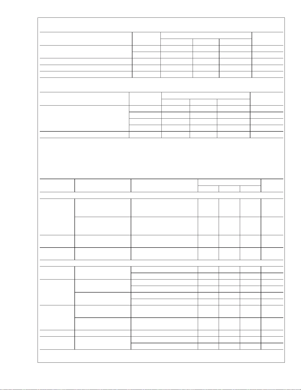
Absolute Maximum Ratings (Notes 1, 2)
LMX2364
Parameter Symbol
Power Supply Voltage V
Voltage on any pin with GND = 0V V
Storage Temperature Range T
Lead Temperature (Solder 4 sec.) T
Min Typ Max
Vcc
V
Vcp
CC
s
L
−0.3 6.5 V
−0.3 6.5 V
−0.3 VCC+ 0.3 V
−65 +150 ˚C
Value
+260 ˚C
Recommended Operating Conditions
Parameter Symbol
Power Supply Voltage V
Operating Temperature T
Note 1: “Absolute Maximum Ratings” indicate limits beyond which damage to the device may occur. Operating Ratings indicate conditions for which the device is
intended to be functional, but do not guarantee specific performance limits. For guaranteed specifications and test conditions, see the Electrical Characteristics. The
guaranteed specifications apply only for the test conditions listed.
Note 2: This Device is a high performance RF integrated circuit with an ESD rating
be done at ESD-free workstations.
Electrical Characteristics (V
VccRF
V
VccIF
V
VcpRF
V
VcpIF
Vcc=VVcp
A
= 3.0V; −40˚C ≤ TA≤ +85˚C except as specified)
Min Typ Max
2.7 5.5 V
V
VccRF
V
VccRF
V
CCIF
−40 +85 ˚C
<
2 kV and is ESD sensitive. Handling and assembly of this device should only
Value
V
VccRF
5.5 V
5.5 V
Units
Units
V
Symbol Parameter Conditions
I
PARAMETERS
CC
I
RF Power Supply Current, RF
CC
Synthesizer, Integer Mode
V
ENIF=VCLK=VDATA=VLE
= HIGH
V
ENRFV
FE=0
Power Supply Current, RF
Synthesizer, Fractional
Mode
ICCIF Power Supply Current, IF
Synthesizer
I
IF PD Power Down Current V
CC
V
ENIF=VCLK,=VDATA=VLE
=HIGH
V
ENRF
FE=1
V
ENRF=VCLK=VDATA=VLE
=HIGH
V
ENIF
ENRF=VENIF
V
CLK=VDATA=VLE
RF SYNTHESIZER PARAMETERS
f
FinRF
Operating Frequency Prescaler = 8/9/12/13 500 1200 MHz
Prescaler = 16/17/20/21 1200 2600 MHz
N Continuous N Divider
Range, Fractional Mode
Continuous N Divider
Range, Integer Mode
Prescaler = 8/9/12/13 40 4095
Prescaler = 16/17/20/21 80 8191
Prescaler = 8/9/12/13 40 266,239
Prescaler = 16/17/20/21 80 532,479
R R Divider Range,
Fractional Mode
R Divider Range, Integer
Mode (Note 3)
f
COMP
p
FinRF
Phase Detector Frequency 15 MHz
RF Input Sensitivity VCC= 3.0V −15 0 dBm
V
= 5.0V −10 0 dBm
CC
= LOW
= LOW
= LOW
=0 V
=LOW
Value
Min Typ Max
5.0 6.3 mA
7.2 8.0 mA
2.4 3.2 mA
5.0 20 µA
1 511
1 64,897
Units
www.national.com 4

LMX2364
Electrical Characteristics (V
Vcc=VVcp
Symbol Parameter Conditions
= 3.0V; −40˚C ≤ TA≤ +85˚C except as specified) (Continued)
Value
Min Typ Max
RF SYNTHESIZER PARAMETERS
I
SRCE RF Charge Pump Source
CPoutRF
Current
I
SINK RF Charge Pump Sink
CPoutRF
Current
I
TRI RF Charge Pump
CPoutRF
TRI-STATE Current
%MIS RF CP Sink vs. CP Source
I
CPoutRF
Mismatch
I
%V RF CP Current vs. CP
CPoutRF
Voltage
RF_CP=0
V
CPoutRF
RF_CP=1
V
CPoutRF
RF_CP=2
V
CPoutRF
RF_CP=3
V
CPoutRF
RF_CP=0
V
CPoutRF
RF_CP=1
V
CPoutRF
RF_CP=2
V
CPoutRF
RF_CP=3
V
CPoutRF
0.5 ≤ V
CPoutRF
V
CPoutRF
= 25˚C
T
A
0.5 ≤ V
CPoutRF
= 25˚C
T
A
=V
=V
=V
=V
=V
=V
=V
=V
=V
VcpRF
VcpRF
VcpRF
VcpRF
VcpRF
VcpRF
VcpRF
VcpRF
VcpRF
≤ V
≤ V
/2
/2
/2
/2
/2
/2
/2
/2
VcpRF
/2
VcpRF
−0.5
−0.5
1mA
4mA
8mA
16 mA
−1 mA
−4 mA
−8 mA
−16 mA
−10.0 10.0 nA
3.5 %
510%
RF_CP=0, 1, or 2
I
%TEMP RF CP Current vs.
CPoutRF
Temperature
VP
CPoutRF
=V
VcpRF
/2
810%
IF SYNTHESIZER PARAMETERS
f
FinIF
N IF Continuous N Divider
Operating Frequency 50 850 MHz
Range
56 262,143
R IF R Divider Range 3 32,767
f
COMP
p
FinIF
I
SRCE IF Charge Pump Source
CPoutIF
I
SINK IF Charge Pump Sink
CPoutIF
I
TRI IF Charge Pump
CPout
%MIS IF CP Sink vs. CP Source
I
CPoutIF
I
%V IF CP Current vs. CP
CPoutIF
I
%TEMP IF CP Current vs.
CPoutIF
Phase Detector Frequency 10 MHz
IF Input Sensitivity 2.7 ≤ V
IF_CP = 0
Current
V
CPoutIF
IF_CP = 1
V
CPoutIF
IF_CP = 0
Current
V
CPoutIF
IF_CP = 1
V
CPoutIF
0.5 ≤ V
TRI-STATE Current
V
CPoutIF
Mismatch
T
A
0.5 ≤ V
Voltage
T
A
V
CPoutIF
Temperature
≤ 5.5V −10 0 dBm
Vcc
100 µA
800 µA
−100 µA
−800 µA
5%
510%
8%
CPout
= 25˚C
CPoutIF
= 25˚C
=V
=V
=V
=V
=V
=V
VcpIF
VcpIF
VcpIF
VcpIF
≤ V
VcpIF
VcpIF
≤ V
/2
/2
/2
/2
VcpIF
/2
VcpIF
/2
−0.5
−0.5
−2.0 2.0 nA
Units
www.national.com5
Electrical Characteristics (V
Vcc=VVcp
= 3.0V; −40˚C ≤ TA≤ +85˚C except as specified) (Continued)
LMX2364
Symbol Parameter Conditions
Min Typ Max
Value
OSCILLATOR PARAMETERS
f
OSC
v
I
OSC
OSC
Oscillator Operating
Frequency
2 110 MHz
Oscillator Sensitivity OSCinRF, OSCinIF 0.5 V
Oscillator Input Current V
OSC=VVcc
V
= 0V −100 µA
OSC
Vcc
100 µA
DIGITAL INTERFACE (DATA, CLK, LE, ENIF, ENRF, Ftest/LD, FLoutRF, FLoutIF)
V
IH
V
IL
I
IH
I
IL
V
OH
V
OL
High-Level Input Voltage 2.7 ≤ V
3.2
≤ 3.2 1.6 V
Vcc
<
V
≤ 5.5 2 V
Vcc
Low-Level Input Voltage 0.4 V
High-Level Input Current VIH=V
CC
−1.0 1.0 µA
Low-Level Input Current VIL= 0 −1.0 1.0 µA
High-Level Output Voltage IOH= −500 µA VCC−0.4 V
Low-Level Output Voltage IOL= 500 µA 0.4 V
MICROWIRE INTERFACE TIMING
T
CS
T
CH
T
CWH
T
CWL
T
ES
T
EW
Data to Clock Set Up Time See Data Input Timing 50 ns
Data to Clock Hold Time See Data Input Timing 10 ns
Clock Pulse Width High See Data Input Timing 50 ns
Clock Pulse Width Low See Data Input Timing 50 ns
Clock to Load Enable Set
Up Time
See Data Input Timing
50 ns
Load Enable Pulse Width See Data Input Timing 50 ns
PHASE NOISE
L
(f) RF RF Synthesizer’s
F1Hz
Normalized Phase Noise
Contribution, Fractional
Mode (Note 4)
RF Synthesizer’s
Normalized Phase Noise
Contribution, Integer Mode
(Note 4)
(f) IF IF Synthesizer’s
L
F1Hz
Normalized Phase Noise
Contribution (Note 4)
Note 3: Some reference divider ratios between the minimum and maximum are not realizable. See the section on R divider programming for more details.
Note 4: Normalized Phase Noise Contribution is defined as: L
measured at an offset frequency, f, ina1HzBandwidth. The offset frequency, f, must be chosen sufficiently smaller than the PLL’s loop bandwidth, yet large enough
to avoid substantial phase noise contribution from the reference source.
RF_OM = 1 (Fractional Mode)
f=3KHz
TCXO Reference Source
RF_CP=1(4mA)
= LOW
V
ENIF
RF_OM = 0 (Integer Mode)
f=3KHz
TCXO Reference Source
RF_CP=2(4mA)
= LOW
V
ENIF
f=3KHz
TCXO Reference Source
IF_CP = 1 (800 mA)
= LOW
V
ENRF
(f) = L(f) – 20·log(N) – 10log(f
F1Hz
COMP
−208 dBc/Hz
−215 dBc/Hz
−212 dBc/Hz
) where L(f) is defined as the single side band phase noise
Units
V
www.national.com 6
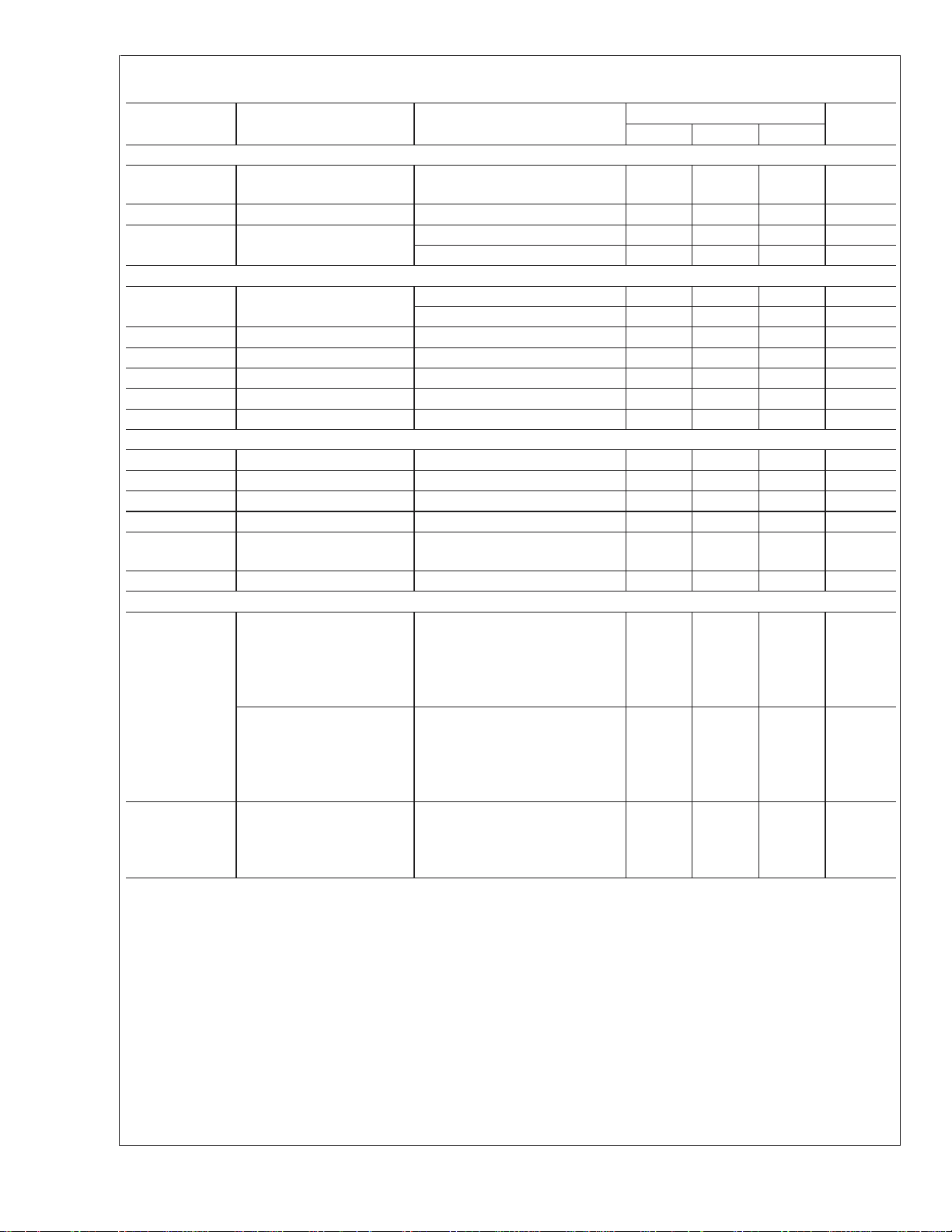
Serial Data Input Timing
20050603
Note: Data is shifted MSB first into the MICROWIRE shift register on the rising edge of the Clock signal. When a rising edge is seen on the LE pulse, these values
are actually loaded into the PLL target registers.
Since the data is clocked in on the rising edge of the LE pulse, the programming time of one register can be eliminated by sending the Data and Clock signals
in advance and delaying the LE pulse until it is desired that the values are to be loaded.
Note: The Serial Data Input Timing is tested using a symmetrical waveform around V
@
VCC=2.7V and 2.6V@VCC= 3.3V.
/2. The test waveform has an edge rate of 0.6 V/ns with amplitudes of 2.2V
CC
LMX2364
www.national.com7

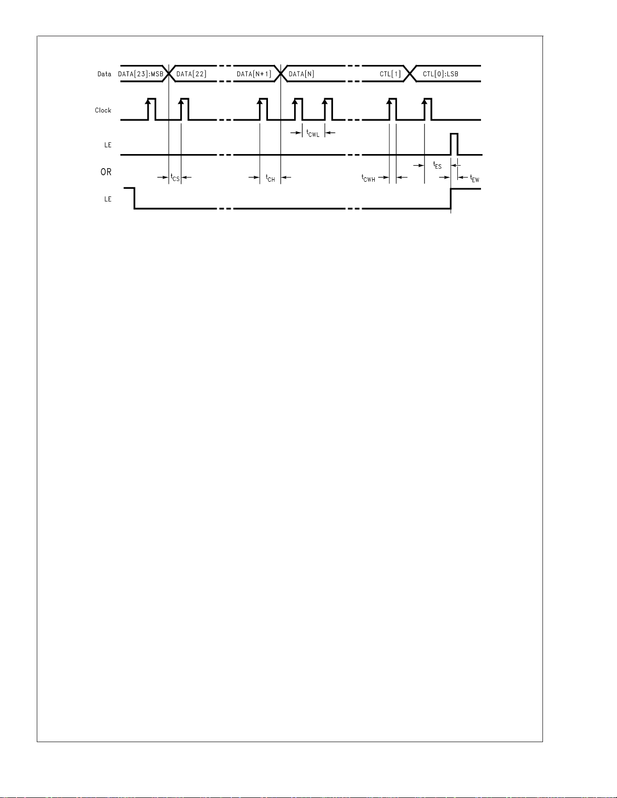
Typical Performance Characteristics
LMX2364
RF PLL 1 Hz Normalized Phase Noise (Fractional Mode)
20050672
IF PLL 1 Hz Normalized Phase Noise
www.national.com 8
20050673
Typical Performance Characteristics (Continued)
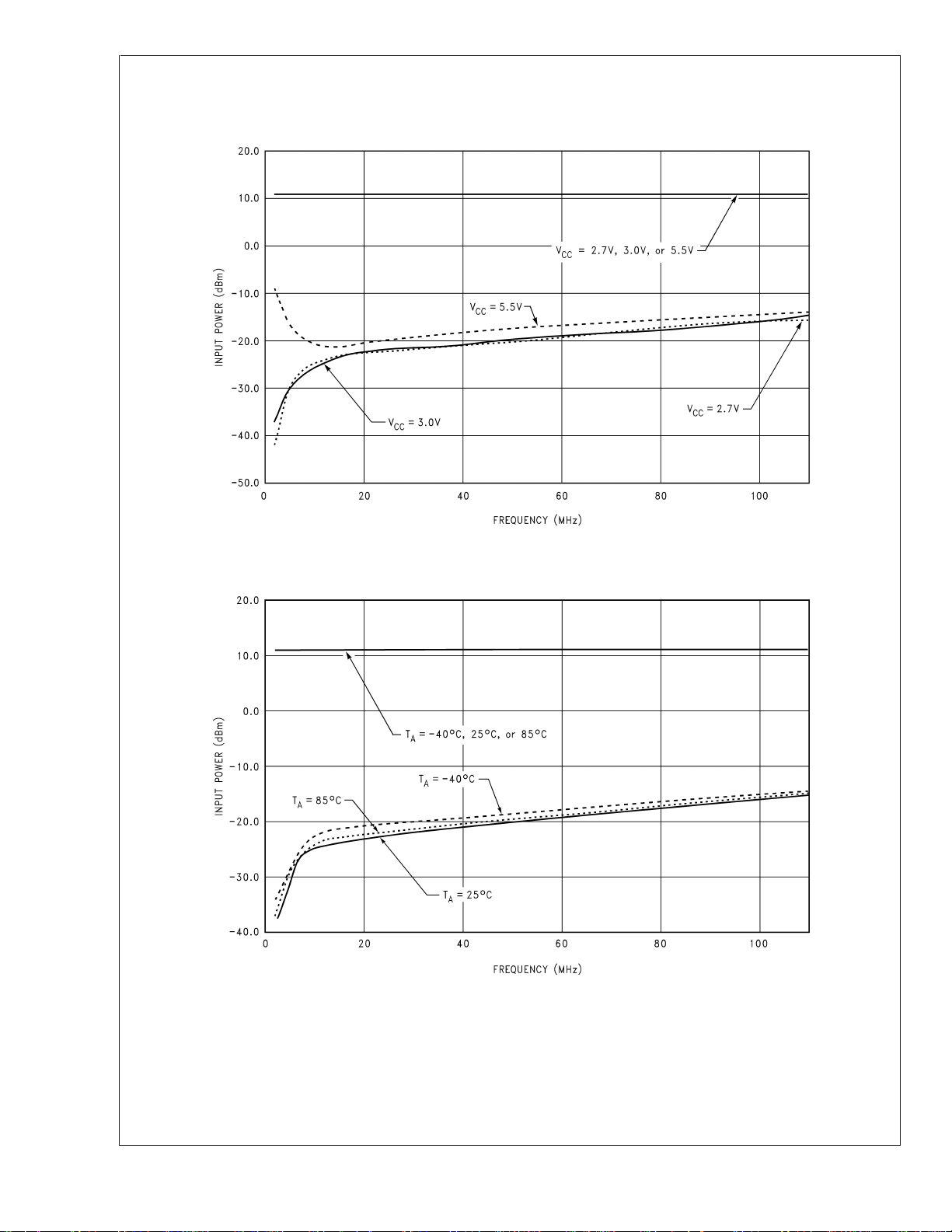
RF N Counter Sensitivity
T
= 25˚C
A
LMX2364
RF N Counter Sensitivity
Vcc = 3.0V
20050645
20050646
www.national.com9

Typical Performance Characteristics (Continued)
LMX2364
IF N Counter Sensitivity
T
= 25˚C
A
IF N Counter Sensitivity
Vcc = 3.0V
20050647
www.national.com 10
20050648

Typical Performance Characteristics (Continued)
OSCinRF Counter Sensitivity
T
= 25˚C
A
LMX2364
OSCinRF Counter Sensitivity
Vcc = 3.0V
20050649
20050650
www.national.com11
Typical Performance Characteristics (Continued)
LMX2364
OSCinIF Counter Sensitivity
T
= 25˚C
A
OSCinIF Counter Sensitivity
Vcc = 3.0V
20050651
www.national.com 12
20050652

Input Impedance: FinRF Pin
CSP Package TSSOP Package
LMX2364
20050653 20050656
FinRF Input Impedance (Ohms)
Frequency (MHz) CSP Package TSSOP Package
Real Imaginary Real Imaginary
500 195 -234 278 -215
750 128 -183 213 -196
1000 98 -152 151 -173
1250 77 -125 96 -133
1500 67 -106 63 -99
1750 59 -92 44 -82
2000 53 -81 35 -62
2250 46 -80 26 -53
2500 43 -67 21 -46
2750 41 -61 17 -36
3000 38 -58 15 -26
www.national.com13

Input Impedance: FinIF Pin
LMX2364
CSP Package TSSOP Package
20050657 20050654
FinIF Input Impedance (ohms)
Frequency (MHz) CSP Package TSSOP Package
Real Imaginary Real Imaginary
100 504 -279 505 -222
200 374 -280 414 -205
300 283 -270 349 -198
400 222 -250 295 -194
500 179 -230 243 -190
600 150 -209 190 -183
700 129 -193 141 -168
800 112 -176 110 -151
900 99 -163 86 -138
1000 98 -151 72 -125
1100 82 -140 65 -118
1200 76 -131 64 -116
www.national.com 14

Input Impedance: OSCinIF Pin
CSP Package TSSOP Package
LMX2364
20050655 20050658
OSCinIF Input Impedance (ohms)
Frequency
(MHz)
10 338 -2741 143 -3239 326 -2100 147 -2400
25 130 -1098 92 -1281 112 -909 84 -1100
50 97 -552 81 -645 86 -463 75 -538
75 89 -366 77 -428 81 -320 71 -372
100 84 -276 75 -322 81 -247 72 -284
110 83 -251 75 -292 82 -230 76 -261
Powered Up Powered Down Powered Up Powered Down
Real Imaginary Real Imaginary Real Imaginary Real Imaginary
CSP Package TSSOP Package
www.national.com15

Typical Performance
Characteristics
LMX2364
Total Current Consumption
RF_OM=1
Powerdown Current
V
ENRF=VENIF
=0V
20050660
20050661
www.national.com 16

Typical Performance Characteristics (Continued)
RF Charge Pump Current
V
= 3.0V
VcpRF
LMX2364
RF Charge Pump Current
= 5.0V
V
VcpRF
20050667
20050668
www.national.com17

Typical Performance Characteristics (Continued)
LMX2364
IF Charge Pump Current
V
= 3.0V
VcpIF
IF Charge Pump Current
= 5.0V
V
VcpIF
20050665
www.national.com 18
20050666

Typical Performance Characteristics (Continued)
Charge Pump Leakage
RF PLL
LMX2364
Charge Pump Leakage
IF PLL
20050664
20050663
www.national.com19

Test Setup Procedures
LMX2364
Sensitivity
20050674
Frequency Input Pin DC Blocking Capacitor Corresponding Counter Default Counter Value MUX Value
OSCinIF 1 nF IF_R/RF_R 5000 9 (IF R/2)
FinIF 100 pF IF_N 5000 10 (IF N/2)
OSCinRF 1 nF RF_R 50 11 (RF R/2)
FinRF 100 pF RF_N 50 12 (RF N/2)
Sensitivity is defined as the power level limits beyond which
the output of the counter being tested is off by 1 Hz or more
of its expected value. It is typically measured over frequency,
voltage, and temperature. In order to test sensitivity, the
MUX[3:0] word is programmed to the appropriate value. The
counter value isthen programmed to a fixed value and a
frequency counter is set to monitor the frequency of this pin.
The expected frequency at the Ftest/LD pin should be the
signal generator frequency divided by twice the corresponding counter value. The factor of two comes in because the
LMX2364 has a flip-flop which divides this frequency by two
to make the duty cycle 50% in order to make it easier to read
with the frequency counter. The frequency counter input
impedance should be set to high impedance.
In order to perform the measurement, the temperature, frequency, and voltage is set to a fixed value and the power
level of the signal is varied. Note that the power level at the
part is assumed to be 4 dB less than the signal generator
power level. This accounts for 1 dB for cable losses and 3 dB
for the pad. The power level range where the frequency is
correct at the Ftest/LD pin to within 1 Hz accuracy is recorded for the sensitivity limits. The temperature, frequency,
and voltage can be varied in order to produce a family of
sensitivity curves. Since this is an open-loop test, the charge
pump is set to TRI-STATE and the unused side of the PLL
(RF or IF) is powered down when not being tested.
For this part, there are actually four frequency input pins,
although there is only one frequency test pin (Ftest/LD). The
conditions specific to each pin are show above.
www.national.com 20

Charge Pump Currents
LMX2364
20050675
The above block diagram shows the test procedure for testing the RF and IF charge pumps. These tests include absolute current level, mismatch, and leakage. In order to measure the charge pump currents, a signal is applied to the high
frequency input pins. The reason for this is to guarantee that
the phase detector gets enough transitions in order to be
able to change states. If no signal is applied, it is possible
that the charge pump current reading will be low due to the
fact that the duty cycle is not 100%. The OSCinIF Pin is tied
to the supply. The charge pump currents can be measured
by simply programming the phase detector to the necessary
polarity. For instance, in order to measure the RF charge
pump current, a 10 MHz signal is applied to the FinRF pin.
The source current can be measured by setting the RF PLL
phase detector to a positive polarity, and the sink current can
be measured by setting the phase detector to a negative
polarity. The IF PLL currents can be measured in a similar
way. Note that the magnitude of the RF and IF PLL charge
pump currents are also controlled by the RF_CP and IF_CP
bits. Once the charge pump currents are known, the mismatch can be calculated as well. In order to measure leakage currents, the charge pump current is set to a TRI-STATE
mode by enabling the counter reset bits. This is RF_RST for
the RF PLL and IF_RST for the IF PLL.
www.national.com21

Input Impedance
LMX2364
20050676
The above block diagram shows the test procedure measuring the input impedance for the LMX2364. This applies to the
FinRF, FinIF, OSCinRF, and OSCinIF pins. The input impedance of the CSP and the TSSOP package should always be
assumed to be different, until proven otherwise. The basic
test procedure is to calibrate the network analyzer, ensure
that the part is powered up, and then measure the input
impedance.
The network analyzer can be calibrated by using either
calibration standards or by soldering resistors directly to the
evaluation board. An open can be implemented by putting no
resistor, a short can be implemented by usinga0ohm
resistor, and a short can be implemented by using two 100
ohm resistors in parallel. Note that no DC blocking capacitor
is used for this test procedure. This is done with the PLL
removed from the PCB. This requires the use of a clamp
down fixture that may not always be generally available. If no
clamp down fixture is available, then this procedure can be
done by calibrating up to the point where the DC blocking
capacitor usually is, and then adding a 0 ohm resistor back
for the actual measurement.
Once that the network analyzer is calibrated, it is necessary
to ensure that the PLL is powered up. This can be done by
toggling the power down bits (RF_PD and IF_PD) and observing that the current consumption indeed increases when
the bit is disabled. Sometimes it may be necessary to apply
a signal to the OSCinIF pin in order to program the part. If
this is necessary, disconnect the signal once it is established
that the part is powered up.
It is useful to know the input impedance of the PLL for the
purposes of debugging RF problems and designing matching networks. Another use of knowing this parameter is make
the trace width on the PCB such that the input impedance of
this trace matches the real part of the input impedance of the
PLL frequency of operation. In general, it is good practice to
keep trace lengths short and make designs that are relatively
resistant to variations in the input impedance of the PLL.
www.national.com 22

Functional Description
1.0 GENERAL
The basic phase-lock-loop (PLL) configuration consists of a
high-stability crystal reference oscillator, a frequency synthesizer such as the National Semiconductor LMX2364, a voltage controlled oscillator (VCO), and a passive loop filter. The
frequency synthesizer includes a phase detector, charge
pump, and programmable frequency dividers. These dividers are the reference [R] and feedback [N] frequency dividers. The VCO frequency is established by dividing the crystal
reference signal down via the R counter to obtain a frequency in order to establish the comparison frequency. This
comparison frequency, f
which compares this signal to another signal, f
back signal. f
is the result of dividing the VCO frequency
N
down by way of the N counter and fractional circuitry. The
phase/frequency detector’s charge pump outputs a current
into the loop filter, which is then converted into the VCO’s
control voltage. The phase/frequency comparator’s function
is to adjust the voltage presented to the VCO until the
feedback signal’s frequency (and phase) match that of the
reference signal. When this ‘phase-locked’ condition exists,
the VCO’s frequency will be N+F times that of the comparison frequency, where N is the integer component of the
divide ratio and F is the fractional component. Fractional
synthesis allows the phase detector frequency to be increased while maintaining the same frequency step size for
channel selection. The division value N is thereby reduced
giving a lower phase noise referred to the phase detector
input, and the comparison frequency is increased allowing
faster switching times.
, is input to the phase detector,
COMP
, the feed-
N
LMX2364
1.1 OPERATING MODES
The LMX2364 RF PLL is a capable of operating as both a
Fractional N synthesizer and an Integer N synthesizer. Operating in Fractional mode is likely to yield the best phase
noise, but Integer mode often yields the lowest spur levels.
The operating mode is determined by the RF_OM[1:0] word.
It is possible to cause this PLL to behave as an integer PLL
in fractional mode by setting the fractional numerator,
RF_FN, to zero and disabling the fractional compensation
that is controlled by the FE bit. However, by actually setting
the part to Integer mode allows the range of the counters to
be extended.
1.2 POWER DOWN
The LMX2364 can be powered down via the two software
bits and the two enable pins. The RF PLL is only powered up
when the ENRF pin is high and the RF_PD bit ( R4[23] ) is
low. In a similar manner, the IF PLL is powered up only when
the ENIF pin is high and the IF_PD bit ( R1[23] ) is low.
1.3 OSCILLATOR
The OSCinRF and OSCinIFpins are used to drive the R
dividers for the RF and IF PLLs. In the case that the OSC Bit
( R6[7] ) is set to 0, the RF R counter is driven by the
OSCinRF pin and the IF R counter is driven independently of
this by the OSCinIF pin. In the case that both R counters are
to be driven with the same frequency, this bit needs to be set
to one. This PLL does not support the use of a crystal in any
mode.
www.national.com23

Programming Description
2.0 INPUT DATA REGISTER
LMX2364
The 24-bit input data register is loaded through the MICROWIRE Interface. The input data register is used to program the control
registers. The data format of the 24-bit data register is shown below. The control bits (CTL[2:0]) decode the internal register
address and the data bits (DATA[21:0]) are used to program various control words for the synthesizer. On the rising edge of LE,
data stored in the input date register is loaded into one of the 8 appropriate latches (selected by control bits). Data is shifted in
MSB first
MSB LSB
DATA [21:0] CTL[2:0]
23 3 2 0
2.1 REGISTER LOCATION TRUTH TABLE
The control bits CTL[2:0] decode the internal register address. The table below shows how the control bits are mapped to the
target control register.
CTL[2:0] Target Control Register
0R0
1R1
2R2
3R3
4R4
5R5
6R6
7 This address is invalid.
2.2 CONTROL REGISTER CONTENT MAP
The control register content map describes how the bits within each control register are allocated to specific control functions. The
bits that are marked “0” should be programmed as such to insure proper device operation. It is important to note that some control
words are dual mapped and take one a different control function depending on the operating mode of the device.
Reg23222120191817161514131211109876543210
DATA[20:0] C2 C1 C0
IF_
R0000
IF_
R1
R20000000 IF_TOC[13:0] 0 1 0
R3
R4
R5 0
R60000000FE0000000
0 0 0 IF_N[16:0] 0 0 1
PD
RF_
RF_PRF_
RST
RF_
PD
CPP
RF_
CSR[1:0]
RST
RF_
CP[1:0]
RF_
OM[1:0]
IF_CPIF_
CPP
CPF[1:0]
IF_R[14:0] 0 0 0
RF_R[8:0] RF_FD[6:0] 0 1 1
RF_N[12:0] RF_FN[6:0] 1 0 0
RF_
RF_TOC[13:0] 1 0 1
PD_
OSC MUX[3:0] 1 1 0
M
www.national.com 24

Programming Description (Continued)
2.3 R0 REGISTER
Reg23222120191817161514131211109876543210
DATA[20:0] C2 C1 C0
IF_
R0000
2.3.1 IF_R[14:0] — R Divider Ratio, IF Synthesizer
The R0 control word is used to configure the 15 Bit R Divider for the IF Synthesizer. Divide ratios ranging from 3 to 32,767 are
supported.
Divide
Ratio
32,767 111111111111111
14131211109876543210
3000000000000011
4000000000000100
••••••••••••••••
2.3.2 IF_CPP — Charge Pump Polarity, IF Synthesizer
This bit controls the polarity of phase detector for the IF synthesizer. It should be set to “1” when the IF VCO has positive tuning
gain, and “0” when the tuning gain is negative.
2.3.3 IF_CP — Charge Pump Gain, IF Synthesizer
This bit controls the charge pump gain for the IF Synthesizer. Set this bit to 0 for low gain mode (100 uA) and a 1 for high gain
mode (800 uA). When FastLock mode is enabled, the charge pump gain is controlled by the FastLock circuit.
RST
IF_CPIF_
CPP
IF_R[14:0] 0 0 0
IF_R[14:0]
LMX2364
2.3.4 IF_RST — Counter Reset, IF Synthesizer
The IF Counter Reset enable bit when activated (IF_RST = 1) allows the reset of both the IF N and R dividers and sets the IF
charge pump to a TRI-STATE condition
®
. Upon powering up, the N counter resumes counting in "close" alignment with the R
counter. The maximum error is one prescaler cycle.
www.national.com25

Programming Description (Continued)
2.4 R1 REGISTER
LMX2364
This register is used to configure the N divider for the IF synthesizer. A single word write to this register is all that is required to
power up and tune the synthesizer to the desired frequency.
Reg23222120191817161514131211109876543210
DATA[20:0] C2 C1 C0
IF_
R1
2.4.1 IF_N[16:0] — N Divider Ratio,IF Synthesizer
The IF_N[16:0] word is used to setup up the N Divider Ratio for the IF synthesizer. The IF N counter is actually a combination of
an IF A counter, IF B counter, and an IF 8/9 prescaler. The relationship between IF_N, IF_B, and IF_A is shown below.
Although the IF_N counter value can created by programming the IF_B and IF_A values, it is easier to simply convert the IF N
counter value into binary and program the entire IF_N[16:0] word in this manner. The fact that the IF N counter has a prescaler
is what puts restrictions on IF_N values less than 56.
0 0 0 IF_N[16:0] 0 0 1
PD
IF_N=8xIF_B + IF_A
IF_N[16:0]
IF_B[13:0] IF_A[2:0]
16151413121110987654321 0
0-23 Divide ratios of less than 24 are not allowed.
24-55 Legal divide ratios in this range are: 24-27, 32-36, 40-45, and 48-54.
56 000000000001110 00
57 000000000001110 01
... ... ... ... ... ... ... ... ... ... ... ... ... ... ... ... ... ...
131071 1111111111111111 1
2.4.2 IF_PD — Power Down, IF Synthesizer
Activation of the IF Synthesizer power down bit results in the disabling of the respective N divider and de-biasing of its respective
Fin inputs (to a high impedance state). The respective R divider functionality also becomes disabled when the power down bit is
activated. The OSCinIF pin reverts to a high impedance state when both RF and IF power down bits are asserted. Power down
forces the respective charge pump and phase comparator logic to a TRI-STATE condition. The MICROWIRE control register
remains active and capable of loading and latching in data during all of the power down modes.
Both synchronous and asynchronous power down modes are supported. The power down mode bit R6[8] is used to select
between synchronous and asynchronous power down. The MICROWIRE control register remains active and capable of loading
and latching in data in either power down mode.
Synchronous Power Down Mode: The IF synthesizer can be synchronously powered down by first setting the power down
mode bit HIGH (R6[8] = 1) and then asserting its power down bit (R1[23] = 1). The power down function is gated by the charge
pump. Once the power down bit is loaded, the part will go into power down mode upon the completion of a charge pump pulse
event.
Asynchronous Power Down Mode: The IF synthesizer can be asynchronously powered down by first setting the power down
mode bit LOW (R6[8] = 0) and then asserting its power down bit (R1[23]] = 1). The power down function is NOT gated by the
charge pump. Once the power down bit is loaded, the part will go into power down mode immediately
www.national.com 26

Programming Description (Continued)
2.5 R2 REGISTER
The R2 Register is used to setup the FastLock circuitry for the IF synthesizer.
Reg23222120191817161514131211109876543210
DATA[20:0] C2 C1 C0
R20000000 IF_TOC[13:0] 0 1 0
2.5.1 IF_TOC[13:0] — FastLock Timeout Counter, IF Synthesizer
The IF_TOC[13:0] word controls the operation of the IF FastLock circuitry as well as the function of the FLoutIF output pin. When
IF_TOC is set to a value between 0 and 3, the IF timeout counter is disabled and the FLoutIF pin operates as a general purpose
I/O pin. When IF_TOC is set to a value between 4 and 16383, the IF FastLock mode is enabled and FLoutIF is utilized as the IF
FastLock output pin. The value programmed into IF_TOC represents the number of phase comparison cycles that the IF
synthesizer will spend in the FastLock state.
IF_TOC[13:0] FastLock Mode
0 Disabled N/A High Impedance
1 Disabled N/A Logic LOW State
2 Manual N/A Logic LOW State. Force IF Charge Pump to 800 µA
3 Disabled 3 Logic HIGH State
4 Enabled 4 FastLock
… Enabled … FastLock
16,383 Enabled 16383 FastLock
FastLock Period
[CP Events]
FLoutIF Pin Functionality
LMX2364
www.national.com27

Programming Description (Continued)
2.6 R3 REGISTER
LMX2364
The R3 register is used to setup the RF R Divider ratio as well as several other control functions related to the RF synthesizer.
Reg23222120191817161514131211109876543210
DATA[20:0] C2 C1 C0
RF_
RST
RF_PRF_
CPP
R3
2.6.1 RF_FD[6:0] — Fractional Denominator, RF Synthesizer
In Fractional Mode, RF_FD[6:0] is used to specify the fractional denominator of the fractional part of the N counter value. Note
that in this mode, values below 32 are not supported. If a fractional denominator between 2 and 32 is desired, the same N counter
value can be achieved by multiplying the fractional numerator and denominator by some constant factor. For instance, 1/16 can
be expressed as 5/80.
In integer mode, the value represented by this bit multiplies both the RF_N and RF_R counter values. If both of these counter
sizes are sufficiently large, it is recommended to set this bit to one. If the counter sizes are too small, this bit can be used to extend
the counter range.
Complete N Divider Value RF_N x RF_FN/RF_FD RF_N x RF_FD + RF_FN
RF_
CP[1:0]
Value
RF_FD[6:0]
0 128 128
1 1 Not Supported (Use Integer Mode Instead)
… … Not Supported ( Use a higher value )
32 32 32
33 33 33
34 34 34
…… …
127 127 127
RF_R[8:0] RF_FD[6:0] 0 1 1
RF_FD
Value
Integer Mode Fractional Mode
[RF_OM = 0] RF_OM = 1
Fractional Mode
(RF_OM=1)
Integer Mode
(RF_OM=0)
R Divider Value RF_R RF_R x RF_FD
See R divider programming (section 2.6.2 ) and N divider programming (Section 2.7.2) for more detailed programming
information.
2.6.2 RF_R[8:0] — R Divider Ratio, RF Synthesizer
RF_R[8:0] is used to specify an integer value from 1 to 511 that is used in calculating the R divider ratio for the RF synthesizer.
In the case that the PLL is operating in fractional mode, the R counter value is simply the value represented by RF_R. However,
in integer mode, the R counter value is calculated by multiplying RF_R by the fractional denominator value.
R (Integer Mode) = RF_R x RF_FD
Since RF_R can take on integer values between 1 – 511 and RF_FD can take on integer values between 1 – 128, this value can
range from 1 - 65408, although prime values between 512 and 65,408 can not be realized.
RF_R[8:0] RF_R
0 Not Supported
11
……
511 511
Value
www.national.com 28

Programming Description (Continued)
2.6.3 RF_CP[1:0] — Charge Pump Gain, RF Synthesizer
The RF_CP word is used to control the charge pump gain for the RF synthesizer. Four different CP gains are supported ranging
from 1 to 16 mA. Note that when RF FastLock mode is enabled and the synthesizer is operating in the FastLock state, the charge
pump gain is controlled by the RF_CPF[1:0] control word. Higher charge pump currents yield slightly better phase noise, but lead
to larger loop filter capacitors and slightly higher current consumption in cases where the comparison frequency is very high.
RF_CP[1:0] Charge Pump Current
01mA
14mA
28mA
316mA
2.6.4 RF_CPP — Phase Detector Polarity, RF Synthesizer
This bit controls the polarity of phase detector for the RF synthesizer. It should be set to one when the chosen RF VCO has
positive tuning gain, and zero when the tuning gain is negative.
2.6.5 RF_P — Prescaler, RF Synthesizer
The RF synthesizer utilizes a selectable quadruple modulus prescaler. RF_P selects between the 8/9/12/13 prescaler and the
16/17/20/21 prescaler as described in the table below.
RF_P[1:0] Selected Prescaler
0 8 (8/9/12/13)
1 16 (16/17/20/21)
LMX2364
2.6.6 RF_RST — Counter Reset, RF Synthesizer
The RF Counter Reset enable bit when activated (RF_RST = 1) allows the reset of both the RF N and RF R dividers. Upon
powering up, the N counter resumes counting in "close" alignment with the R counter. The maximum error is one prescaler cycle.
www.national.com29

Programming Description (Continued)
2.7 R4 REGISTER
LMX2364
This register is used to setup the N divider for the RF Synthesizer. A single word write to this register is all that is required to power
up and tune the RF synthesizer to the desired frequency.
Reg23222120191817161514131211109876543210
DATA[20:0] C2 C1 C0
RF_
R4
PD
2.7.1 RF_FN — Fractional Numerator, RF Synthesizer
In the case that the PLL is operating in fractional mode (RF_OM=1), RF_FN[6:0] specifies the fractional numerator of the
complete N counter value of the RF PLL. In the case that the PLL is operating in integer mode (RF_OM=0), RF_FN adds to the
total value of the N counter.
Operating Mode RF N Divider Value Calculation
Fractional Mode (RF_OM=1) RF_N +RF_FN/RF_FD
Integer Mode (RF_OM=0) RF_N x RF_FD + RF_FN
2.7.2 RF_N[12:0] — N Divider Ratio, RF Synthesizer
RF_N[12:0] specifies an integer value that is used in calculating the N divider ratio for the RF synthesizer. In the case the part is
operating in fractional mode, it value is the N divider ratio. In the case the part is operating in integer mode, this number is used
in conjunction with the RF_FD and RF_FN values to calculate the N divider value. The range of values supported is dependant
on the selected prescaler. When the 8/9/12/13 prescaler is selected, RF_N value can range from 40 to 4095. When the
16/17/20/21 prescaler is selected, the RF_N value can range from 80 to 8191. The following tables describe how to program a
specific value of RF_N for a given prescaler.
The RF_N value is actually created using a prescaler, C counter, B counter, and an A counter. If RF_P = 16, then the RF_N[12:0]
word is just the binary representation of the desired value. If RF_P = 8, then the case is similiar, except that the third LSB is
disregarded in all calculations. The relationship between RF_N, RF_P, RF_A, RF_B, and RF_C is shown below.
RF_N[12:0] RF_FN[6:0] 1 0 0
RF_N = RF_PxRF_C +4xRF_B + RF_A
RF_N[12:0] Programming with RF_P = 16
RF_N[12:0]
121110987654 3 2 1 0
RF_C[8:0] RF_B [1:0] RF_A[1:0]
0–47 Values from 0–47 are not allowed.
Some of these N values are allowed, others are illegal divide ratios and not allowed.
48–79 Legal Divide Ratios in Fractional Mode: 48–49, 52–53, 64–66, 68–70, 72–74, 76–78
Legal Divide Ratios in Integer Mode: All these values are legal in integer mode.
80 0 0 0 000101 0 0 0 0
81 0 0 0 000101 0 0 0 1
…
8191 1 1 1 111111 1 1 1 1
RF_N[12:0] Programming with RF_P = 8
RF_N[12:0]
121110987654 3 2 1 0
RF_C[8:0] RF_B[1:0] RF_A[1:0]
0–23 Values from 0– 23 are not allowed.
Some of these N values are allowed, others are illegal divide ratios and not allowed.
24–39 Legal Divide Ratios in Fractional Mode: 24–25, 28– 29, 32– 34, 36– 38
Legal Divide Ratios in Integer Mode: All these values are legal in integer mode.
40 0 0 0 000011 X 0 0 0
41 0 0 0 000011 X 0 0 1
…
4095 1 1 1 111111 X 1 1 1
www.national.com 30

Programming Description (Continued)
2.7.3 RF_PD — RF Synthesizer Power Down
Activation of the RF Synthesizer power down bit results in the disabling of the respective N divider and de-biasing of its respective
Fin inputs (to a high impedance state). The respective R divider functionality also becomes disabled when the power down bit is
activated. The OSCinRF pin reverts to a high impedance state when both RF and IF power down bits are asserted. Power down
forces the respective charge pump and phase comparator logic to a TRI-STATE condition. The MICROWIRE control register
remains active and capable of loading and latching in data during all of the power down modes.
Both synchronous and asynchronous power down modes are available with the LMX2364 in order to adapt to different types of
applications. The power down mode bit R6[8] is used to select between synchronous and asynchronous power down. The
MICROWIRE control register remains active and capable of loading and latching in data in either power down mode.
Synchronous Power down Mode: The RF synthesizer can be synchronously powered down by first setting the power down
mode bit HIGH (R6[8] = 1) and then asserting its power down bit (R4[23] = 1). The power down function is gated by the charge
pump. Once the power down bit is loaded, the part will go into power down mode upon the completion of a charge pump pulse
event.
Asynchronous Power down Mode: The RF synthesizer can be asynchronously powered down by first setting the power down
mode bit LOW (R6[8] = 0) and then asserting its power down bit (R4[23]] = 1). The power down function is NOT gated by the
charge pump. Once the power down bit is loaded, the part will go into power down mode immediately
LMX2364
www.national.com31

Programming Description (Continued)
2.8 R5 REGISTER
LMX2364
The R5 Register is used to setup and control the FastLock circuitry for the RF synthesizer.
Reg23222120191817161514131211109876543210
DATA[20:0] C2 C1 C0
R5 0
RF_
CSR[1:0]
2.8.1 RF_TOC[13:0] — FastLock Timeout Counter, RF Synthesizer
The RF_TOC[13:0] word controls the operation of the RF FastLock circuitry as well as the function of the FLoutRF output pin.
When RF_TOC is set to a value between 0 and 3, the RF timeout counter is disabled and the FLoutRF pin operates as a general
purpose I/O pin. When RF_TOC is set to a value between 4 and 16383, the RF FastLock mode is enabled and FLoutRF is utilized
as the RF FastLock output pin. The value programmed into RF_TOC represents the number of phase comparison cycles that the
RF synthesizer will spend in the FastLock state.
RF_TOC[13:0] FastLock Mode
0 Disabled N/A High Impedance
1 Disabled N/A Logic LOW State
2 Manual N/A Logic LOW State. Force RF Change Pump to 16 mA
3 Disabled 3 Logic HIGH State
4 Enabled 4 FastLock
… Enabled … FastLock
16,383 Enabled 16383 FastLock
2.8.2 RF_CPF[1:0] — FastLock Charge Pump Gain, RF Synthesizer
The RF_CPF[1:0] word is used to control the charge pump gain for the RF synthesizer when FastLock is enabled and engaged.
Four different CP gains are supported ranging from 1 to 16 mA. Note that when RF FastLock mode is disengaged or disabled the
charge pump gain is controlled by RF_CP[1:0].
RF_
OM[1:0]
RF_CPF[1:0] Charge Pump Current
RF_
CPF[1:0]
FastLock Period
[CP Events]
01mA
14mA
28mA
316mA
RF_TOC[13:0] 1 0 1
FLoutRF Pin Functionality
2.8.3 RF_OM[1:0] — RF Synthesizer Operating Mode
RF_OM[1:0] controls the operating mode of the RF synthesizer. The various operating modes are described below:
RF Synthesizer Operating Mode Descriptions
RF_OM FE<R6[16]
0 0 Integer RF synthesizer always operates as an Integer N PLL
1 1 Fractional RF synthesizer always operates as a Fractional N PLL
2 X Reserved Do Not use this mode
3 X Reserved Do Not use this mode.
>
Operating Mode Operating Mode Description
Note that the Fractional Enable Bit, FE (R6[16]) needs to be set appropriately. Enabling the fractional compensation in Integer
mode always degrades performance. It is generally recommended to enable it in fractional mode, although there may be some
rare exceptions that it may be set to 0.
2.8.4 RF_CSR[1:0] — Cycle Slip Reduction Control, RF Synthesizer
RF_CSR[1:0] controls the operation of the cycle slip reduction circuitry. This circuit can be used eliminate the occurrence of phase
detector cycle slips when operating in Fractional Mode (RF_OM = 1). When operating in integer mode,the cycle slip reduction
circuitry should be disabled by setting RF_CSR = 0.
RF_CSR CSR State Sample Rate Reduction Factor
0 Disabled N/A
1 Enabled 1/2
2 Enabled 1/4
3 Enabled 1/8
www.national.com 32

Programming Description (Continued)
2.9 R6 REGISTER
Reg23222120191817161514131211109876543210
DATA[20:0] C2 C1 C0
R60000000FE0000000
2.9.1 MUX[3:0] — Coltrol Word for the Ftest/LD Pin
The MUX[3:0] control word is used to determine the function of the Ftest/LD output pin. The pin can be setup as a generalpurpose CMOS TRI-STATE I/O pin, a digital filtered lock detect pin, an analog lock detect pin (push-pull or open drain output), or
used to view the output of the variousR&Ndividers.
MUX[3:0] Ftest/LD Output Pin Function Output Type
0 0 0 0 Disabled High Impedance
0 0 0 1 General Purpose I/O. Logic HIGH Output Push-Pull
0 0 1 0 General Purpose I/O. Logic LOW Output Push-Pull
0 0 1 1 RF & IF Analog Lock Detect (Width of
0 1 0 0 RF Analog Lock Detect (Width of narrow
0 1 0 1 IF Analog Lock Detect (Width of narrow
0 1 1 0 RF & IF Digital Lock Detect (High = Lock) Push-Pull
0 1 1 1 RF Digital Lock Detect (High = Lock) Push-Pull
1 0 0 0 IF Digital Lock Detect (High = Lock) Push-Pull
1 0 0 1 RF & IF Analog Lock Detect (Width of
1 0 1 0 RF Analog Lock Detect (Width of narrow
1 0 1 1 IF Analog Lock Detect (Width of narrow
1 1 0 0 IF R Divider/2 (Output is divided by 2 to
1 1 0 1 IF N Divider/2 (Output is divided by 2 to
1 1 1 0 RF R Divider/2 (Output is divided by 2 to
1 1 1 1 RF N Divider/2 (Output is divided by 2 to
narrow low pulses determines lock)
low pulses determines lock)
low pulses determines lock)
narrow low pulses determines lock)
low pulses determines lock)
low pulses determines lock)
simplify testing)
simplify testing)
simplify testing)
simplify testing)
PD_
OSC MUX[3:0] 1 1 0
M
Open-Drain
Open-Drain
Open-Drain
Push-Pull
Push-Pull
Push-Pull
Push-Pull
Push-Pull
Push-Pull
Push-Pull
LMX2364
2.9.2 OSC — Single Resonator Mode
The OSC bit selects whether the oscillator input pins OSCinIF and OSCinRF drive the IF and RF R dividers separately or by a
common input signal path. When OSC is set to 0, the OSCinIF pin drives the IF R divider while the OSCinRF pin drives the RF
R divider. When the OSC bit is set to “1” the OSCinIF pin drives both the RF R and IF R counters. Note that setting the OSC mode
to “1” does not allow the use of a crystal. This part does not include the inverter for use in construction of a crystal oscillator.
2.9.3 PD_M — Power Down Mode
This bit determines if a power down event for either synthesizer will be handled synchronously or asynchronously with respect to
a charge pump event. Synchronous powerdown means that the PLL does not power down until the charge pump turns off.
Asynchronous powerdown means that the PLL powers down, regardless of the charge pump state. When set to one,
synchronous mode is enabled. When set to 0, asynchronous mode is enabled. The setting of this bit applies to both the RF & IF
synthesizers.
2.9.4 FE — Fractional Compensation Enable
For integer mode (RF_OM=0)mode, this bit should always be set to 0. For fractional mode (RF_OM = 1), this bit should be set
to 1 for the best fractional spurs. However, there may be applications using fractional mode where it would be beneficial to set
this bit to 0. Disabling this bit will drastically degrade the fractional spurs, but will also result in a small improvement in phase
noise, which may be practical for some applications.
FE
0 Disabled Default State 0 dB 0 dB
1 Enabled Illegal State 20 dB 7 dB
Fractional
Compensation
Circuitry
Integer
Mode
Approximate Spur
Improvement
Fractional Mode
Approximate Phase
Noise
Degradation
www.national.com33

Supplemental Information
3.0 USE OF THE DIGITAL LOCK DETECT FUNCTION
LMX2364
The Lock Detect Digital Filter compares the difference between the phase of the inputs of the phase detector to a RC
generated delay of approximately 15nS. To enter the locked
state (Lock = HIGH) the phase error must be less than the
15nS RC delay for 5 consecutive reference cycles. Once in
lock (Lock = HIGH), the RC delay is changed to approximately 30nS. To exit the locked state (Lock = LOW), the
phase error must become greater than the 30nS RC delay.
When the PLL is in the power down mode, Lock is forced
LOW. A flow chart of the digital filter is shown below.
www.national.com 34
20050604

Supplemental Information (Continued)
3.1 PCB LAYOUT CONSIDERATIONS
Power Supply Pins: For these pins, it is recommended that
these be filtered by taking a series 18 ohm resistor and then
placing two capacitors shunt to ground, thus creating a
lowpass filter.Although theoretically, it makes sense to make
these capacitors as large as possible, the ESR ( Equivalent
Series Resistance ) is greater for larger capacitors. It is
therefore recommended to provide two capacitors of very
different sizes for the best filtering. 0.1 uF and 100 pF are
typical values. The charge pump supply pins in particular are
vulnerable to power supply noise.
High Frequency Input Pins, FinRF and FinIF: The signal
path from the VCO to the PLL is sensitive to matching and
layout, therefore creating unique challenges fro board layout. It is generally recommended that the VCO output go
through a resistive pad and then through a DC blocking
capacitor before it gets to these high frequency input pins. If
the trace length is sufficiently short (
length ), then the pad may not be necessary, however, a
series resistor of about 39 ohms is still recommended to
isolate the PLL from the VCO. The DC blocking capacitor
should be chosen at least to be 100 pF. It may turn out that
the frequency in this trace is above the self-resonant frequency of the capacitor, but since the input impedance of the
PLL tends to be capacitive, it actually be a benefit to exceed
the self-resonant frequency. The pad and the DC blocking
capacitor should be placed as close to the PLL as possible
<
1/10th of a wave-
LMX2364
Complimentary High Frequency Pins, FinRF* and FinIF*:
These outputs may be used to drive the PLL differentially,
but it is very common to drive the PLL in a single ended
fashion. These capacitors should be chosen such that the
impedance, including the ESR of the capacitor, is as close to
an AC short as possible at the operating frequency of the
PLL. 100 pF is a typical value.
3.2 FASTLOCK AND CYCLE SLIP REDUCTION
CIRCUITRY OPERATION
The LMX2364 has enhanced features for FastLock operation. When the PLL is switching frequencies, the charge
pump current and comparison frequencies may be adjusted.
The purpose of increasing the charge pump current is to
increase the loop bandwidth. The purpose of reducing the
comparison frequency is to combat cycle slipping. If these
two parameters are not changed by the same ratio, then it is
necessary to switch in a resistor in order to keep the loop
filter optimized. Furthermore, it may be difficult in this case to
keep loop filters of higher than second order well optimized
during FastLock in these cases. The timeout counter controls how long the change in charge pump current and/or
comparison frequency is active. One also needs to realize
that there is a frequency glitch that is caused when any sort
of FastLock or Cycle Slip Reduction is disengaged. This
frequency glitch is application specific. In this case the table
below shows all the possible permutations for using the
FastLock and cycle slip reduction circuitry.
Keep Comparison Frequency
the Same
Increase Charge Pump
Current
Keep Charge Pump Current
the Same
Decrease Charge Pump
Current
Note: If the charge pump current and cycle slip reduction
circuitry are engaged in the same proportion, then it is not
necessary to switch in a FastLock resistor and the loop filter
will be optimized for both normal mode and FastLocking
Classical Fastlock
This mode allows the loop
bandwidth to be increased
during FastLock and then
switched back to normal after
FastLock is disengaged.
Operation Without Fastlock
This mode is essentially not
using fastlock at all.
Illegal Mode
This mode degrades performance and should never be used.
Decrease Comparison Frequency
(RF Side Only)
CSR/Fastlock Combination
This is the recommended way to use CSR.
If the charge pump gain is used to balance
the change in loop gain due to the lower
comparision frequency, no fastlock resistor
is necessary.
CSR Only
In general, this mode is not recommended,
but it may be practical in some rare
situations.
mode. For third and fourth order filters which have problems
with cycle slipping, this may prove to be the optimal choice of
settings.
www.national.com35

Supplemental Information (Continued)
3.3 DETERMINING THE THEORETICAL LOCK TIME
LMX2364
IMPROVEMENT AND FASTLOCK RESISTOR, R2
The loop bandwidth multiplier, K, is necessary in order to
determine the theoretical impact of FastLock/CSR on the
loop bandwidth and also which resistor should be switched
in parallel with the loop filter resistor R2. K = K_Kphi x
K_Fcomp where K is the loop gain multiplier K_Kphi and
K_Fcomp are the ratio of the FastLock currents and comparison frequencies to their steady state conditions. Note
that this should always be greater than or equal to one.
K_Fcomp is the ratio of the FastLock comparison frequency
to the steady state comparison frequency. If this ratio is less
than one, this implies that the CSR is being used.
When K is greater than one, is necessary to switch a FastLock resistor, R2’, in parallel with R2 in order to keep the
loop filter optimized and maintain the same phase margin.
After the PLL has achieved a frequency that is sufficiently
close to the desired frequency, the resistor R2’ is disengaged
and the charge pump current is and comparison frequency
are returned to normal. Of special concern is the glitch that is
caused when the resistor R2’ is disengaged. This glitch can
take up a significant portion of the lock time. The LMX2364
has enhanced switching circuitry to minimize this glitch and
therefore improve the lock time.
20050640
The change in loop bandwidth is dependent upon the loop
gain multiplier, K. The theoretical improvement in lock time is
given below, but the actual improvement will be less than this
due to the glitch that is caused by disengaging FastLock.
The theoretical improvement is given to show an upper
bound on what improvement is possible with FastLock. In
the case that K
* These modes of operation are generally not recommended
3.4 USING FASTLOCK AND CSR TO AVOID CYCLE
SLIPPING
In the case that the comparison frequency is very large ( ie.
70x)oftheloop bandwidth, cycle slipping may occur when
an instantaneous phase error is presented to the phase
<
1, this implies the CSR is being engaged
Loop Gain Multiplier,
K
1:8* 0.35 open x 2.828
1:4* 0.50 open x 2.000
1:2* 0.71 open x 1.414
1:1 1.00 open x 1.000
2:1 1.41 R2/0.41 x 0.707
4:1 2.00 R2 x 0.500
8:1 2.83 R2/1.83 x 0.354
16:1 4.00 R2/3.00 x 0.250
K:1
FastLock Loop
Bandwidth/Steady
State Loop
and that the theoretical lock time will be degraded. However,
since this mode reduces or eliminates cycle slipping, the
actual lock time may be better in cases where the loop
bandwidth is small relative to the comparison frequency.
Realize that the theoretical lock time multiplier does not
account for the FastLock/CSR disengagement glitch, which
is most severe for larger values of K.
R2’ Value
detector. This can be reduced by increasing the loop bandwidth during frequency aquisition, decreasing the comparison frequency during frequency acquisition, or some combination of the these. If increasing the loop bandwidth during
frequency acquisition is not sufficient to reduce cycle slipping, the LMX2364 also has a routine to decrease the comparison frequency.
Theoretical Lock
Time Multiplier
1/
www.national.com 36

Supplemental Information (Continued)
3.5 RF PLL FASTLOCK REFERENCE TABLE
The table below shows most of the trade offs involved in
choosing a steady-state charge pump current (RF_CP), the
Parameter Advantages to Choosing Smaller Advantages to Choosing Larger
RF_CP 1. Allows capacitors in loop filter to be smaller
values making it easier to find physically
smaller components and components with
better dielectric properties.
2. Allows a larger loop bandwidth multiplier for
FastLock, or a higher cycle slip reduction
factor.
RF_CPF The only reason not to always choose this to
16 mA is to make it such that no FastLock
resistor is required for FastLock. For 3rd and
4th order filters, it is not possible to keep the
filter perfectly optimized by simply switching in
a resistor for FastLock.
RF_CSR Do not choose this any larger than necessary
to eliminate cycle slipping. Keeping this small
allows a larger loop bandwidth multiplier for
FastLock.
LMX2364
FastLock charge pump current (RF_CPF[1:0]), and the
Cycle Slip Reduction Factor CSR.
Phase noise, especially within the loop
bandwidth of the system will be slightly worse
for lower charge pump currents. If the charge
pump gain is at least 4 mA, most of the
phase noise benefit will be realized.
This allows the maximum possible benefit for
FastLock.
This will eliminate cycle slips better.
3.6 CAPACITOR DIELECTRIC CONSIDERATIONS
The LMX2364 has a high fractional modulus and high
charge pump gain for the lowest possible phase noise. One
consideration is that the reduced N value and higher charge
pump may cause the capacitors in the loop filter to become
larger in value. For larger capacitor values, it is common to
have a trade-off between capacitor dielectric quality and
physical size. Using film capacitors or NP0/CG0 capacitors
yields the best possible lock times, where as using X7R or
Z5R capacitors can increase lock time by 0 – 500%. In
general, designs with higher comparison frequencies tend to
be less succeptible to degradations in lock time due to
capacitor dielectric effects. Capacitor dielectrics have very
little impact on phase noise or spurs. Although the use of
lesser quality dielectric capacitors may be unavoidable in
many circumstances, allowing a larger footprint for the loop
filter capacitors, using a lower charge pump current, and
reducing the fractional modulus are all ways to reduce capacitor values.
www.national.com37

Physical Dimensions inches (millimeters) unless otherwise noted
LMX2364
Thin Shrink Small Outline (TSSOP) Package
Order Number LMX2364TM (Rail)
Order Number LMX2364TMX (Tape and Reel)
NS Package Number MTC24
www.national.com 38

Physical Dimensions inches (millimeters) unless otherwise noted (Continued)
LMX2364 2.6 GHz PLLatinum Fractional RF Frequency Synthesizer with 850 MHz Integer-N IF
Frequency Synthesizer
Ultra Thin Chip Scale Package (SLE)
For Tape and Reel (2500 Units per Reel)
Order Number LMX2364SLEX
NS Package Number SLE24A
LIFE SUPPORT POLICY
NATIONAL’S PRODUCTS ARE NOT AUTHORIZED FOR USE AS CRITICAL COMPONENTS IN LIFE SUPPORT
DEVICES OR SYSTEMS WITHOUT THE EXPRESS WRITTEN APPROVAL OF THE PRESIDENT AND GENERAL
COUNSEL OF NATIONAL SEMICONDUCTOR CORPORATION. As used herein:
1. Life support devices or systems are devices or
systems which, (a) are intended for surgical implant
into the body, or (b) support or sustain life, and
whose failure to perform when properly used in
accordance with instructions for use provided in the
2. A critical component is any component of a life
support device or system whose failure to perform
can be reasonably expected to cause the failure of
the life support device or system, or to affect its
safety or effectiveness.
labeling, can be reasonably expected to result in a
significant injury to the user.
National Semiconductor
Americas Customer
Support Center
Email: new.feedback@nsc.com
Tel: 1-800-272-9959
www.national.com
National Semiconductor
Europe Customer Support Center
Fax: +49 (0) 180-530 85 86
Email: europe.support@nsc.com
Deutsch Tel: +49 (0) 69 9508 6208
English Tel: +44 (0) 870 24 0 2171
Français Tel: +33 (0) 1 41 91 8790
National Semiconductor
Asia Pacific Customer
Support Center
Email: ap.support@nsc.com
National Semiconductor
Japan Customer Support Center
Fax: 81-3-5639-7507
Email: jpn.feedback@nsc.com
Tel: 81-3-5639-7560
National does not assume any responsibility for use of any circuitry described, no circuit patent licenses are implied and National reserves the right at any time without notice to change said circuitry and specifications.
 Loading...